EP1557560B1 - Dynamische Steuerung eines Leistungstransistors bei Hochspannungsanwendungen - Google Patents
Dynamische Steuerung eines Leistungstransistors bei Hochspannungsanwendungen Download PDFInfo
- Publication number
- EP1557560B1 EP1557560B1 EP04425035A EP04425035A EP1557560B1 EP 1557560 B1 EP1557560 B1 EP 1557560B1 EP 04425035 A EP04425035 A EP 04425035A EP 04425035 A EP04425035 A EP 04425035A EP 1557560 B1 EP1557560 B1 EP 1557560B1
- Authority
- EP
- European Patent Office
- Prior art keywords
- transistor
- terminal
- jfet
- circuit
- voltage
- Prior art date
- Legal status (The legal status is an assumption and is not a legal conclusion. Google has not performed a legal analysis and makes no representation as to the accuracy of the status listed.)
- Expired - Lifetime
Links
- 238000005516 engineering process Methods 0.000 description 10
- 239000000758 substrate Substances 0.000 description 5
- 210000000746 body region Anatomy 0.000 description 4
- 239000004065 semiconductor Substances 0.000 description 4
- 238000004804 winding Methods 0.000 description 4
- XUIMIQQOPSSXEZ-UHFFFAOYSA-N Silicon Chemical compound [Si] XUIMIQQOPSSXEZ-UHFFFAOYSA-N 0.000 description 2
- 238000010586 diagram Methods 0.000 description 2
- 239000002184 metal Substances 0.000 description 2
- 230000010355 oscillation Effects 0.000 description 2
- 229910052710 silicon Inorganic materials 0.000 description 2
- 239000010703 silicon Substances 0.000 description 2
- 238000004088 simulation Methods 0.000 description 2
- 239000011800 void material Substances 0.000 description 2
- 235000010724 Wisteria floribunda Nutrition 0.000 description 1
- 238000002485 combustion reaction Methods 0.000 description 1
- 230000007423 decrease Effects 0.000 description 1
- 239000000700 radioactive tracer Substances 0.000 description 1
- 230000006641 stabilisation Effects 0.000 description 1
Images




Classifications
-
- H—ELECTRICITY
- H03—ELECTRONIC CIRCUITRY
- H03K—PULSE TECHNIQUE
- H03K17/00—Electronic switching or gating, i.e. not by contact-making and –breaking
- H03K17/08—Modifications for protecting switching circuit against overcurrent or overvoltage
- H03K17/082—Modifications for protecting switching circuit against overcurrent or overvoltage by feedback from the output to the control circuit
- H03K17/0828—Modifications for protecting switching circuit against overcurrent or overvoltage by feedback from the output to the control circuit in composite switches
-
- F—MECHANICAL ENGINEERING; LIGHTING; HEATING; WEAPONS; BLASTING
- F02—COMBUSTION ENGINES; HOT-GAS OR COMBUSTION-PRODUCT ENGINE PLANTS
- F02P—IGNITION, OTHER THAN COMPRESSION IGNITION, FOR INTERNAL-COMBUSTION ENGINES; TESTING OF IGNITION TIMING IN COMPRESSION-IGNITION ENGINES
- F02P3/00—Other installations
- F02P3/02—Other installations having inductive energy storage, e.g. arrangements of induction coils
- F02P3/04—Layout of circuits
- F02P3/0407—Opening or closing the primary coil circuit with electronic switching means
- F02P3/0435—Opening or closing the primary coil circuit with electronic switching means with semiconductor devices
-
- F—MECHANICAL ENGINEERING; LIGHTING; HEATING; WEAPONS; BLASTING
- F02—COMBUSTION ENGINES; HOT-GAS OR COMBUSTION-PRODUCT ENGINE PLANTS
- F02D—CONTROLLING COMBUSTION ENGINES
- F02D41/00—Electrical control of supply of combustible mixture or its constituents
- F02D41/20—Output circuits, e.g. for controlling currents in command coils
- F02D2041/2068—Output circuits, e.g. for controlling currents in command coils characterised by the circuit design or special circuit elements
- F02D2041/2075—Type of transistors or particular use thereof
Definitions
- the present invention relates to a circuit for dynamic control of a power transistor in applications for high voltage.
- the invention relates to a circuit for dynamic control of a power transistor in applications for high voltage comprising a power transistor with a conduction terminal connected to a load and a control terminal receiving a driving signal from a driver block activated by a trigger signal, received on a circuit input terminal.
- the invention particularly relates, but not exclusively, to a circuit for dynamic control of a power transistor of the IGBT type, in applications for high voltage, and the following description is made with reference to this field of application for convenience of illustration only.
- Microprocessor-driven control systems for electronic ignition are known. These systems, in their most general form, allow a spark to be generated on a sparking plug associated to an internal-combustion engine.
- control circuit for electronic ignition globally indicated with 1, is schematically shown in figure 1.
- the control circuit 1 receives a trigger pulse Vin produced for example by a microprocessor (not shown in the figure) and applied to an input terminal IN connected to a driving terminal of an operated switch SW1.
- the switch SW1 is inserted between a first voltage reference, particularly a supply voltage reference Vbat, and a second voltage reference, particularly a ground GND.
- the switch SW1 is also connected to a primary coil winding 1A, connected in turn to said supply voltage reference Vbat and to an ignition sparking plug 1B.
- the trigger pulse Vin determines the charging time of the primary coil winding 1A, closing the switch SW 1 through which a current I COIL flows, as shown in figure 2.
- the trigger signal Vin has a low value and, consequently, the switch SW1 is open, keeping also the current value I COIL low and the voltage V SW1 is equal to the voltage Vbatt.
- the microprocessor brings the trigger signal Vin at a high value which, closing the switch SW1, allows the current I COIL to flow in the coil winding 1A.
- the trigger signal Vin is kept high until a time t3.
- the coil current I COIL increases with a slope trend until it reaches a maximum value in correspondence with a time t2 being lower than t3, remaining thus at this value until the time t3.
- the trigger signal Vin goes back to the low state and it consequently opens the switch SW1.
- the voltage Vswi at the ends of the switch instantaneously reaches a high value.
- An overvoltage thus occurs on the primary coil winding 1A which, transferring to the secondary through the coil turn ratio, generates a spark on the sparking plug 1B.
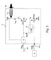
- control circuit 1 of figure 1 timed as described in figure 2, is shown in figure 3, wherein the switch SW1 is realised by means of a power element, particularly an IGBT transistor.
- the control circuit 2 for electronic ignition receives on a first input terminal IN1 the trigger pulse Vin produced by a microprocessor not shown in the figure.
- the control circuit 2 comprises a power element, particularly an IGBT transistor TR1 used as switch, comprised between the supply voltage reference Vbat and the ground GND.
- the transistor TR1 has a first conduction terminal, particularly the collector terminal C, coupled to a supply voltage reference Vbat by means of the coil 1A, a second conduction terminal, particularly the emitter terminal E, coupled to the ground GND by means of a sensing resistance Rsen, as well as a control terminal, particularly a gate terminal G1 connected, by means of a driver block 4, to the first input terminal of the control circuit 2.
- the driver block 4 is also connected to the supply voltage reference Vbat.
- the control circuit 2 also comprises a current limiting block 5 inserted between the control terminal G1 and the emitter terminal E of the transistor TR 1 and essentially comprising an operational amplifier OP1.
- the operation amplifier OP1 is a fed-back non inverting amplifier having a non inverting input terminal (+) connected to the emitter terminal E, an inverting input terminal (-) connected to the reference voltage generator 3 and an output terminal connected to the control terminal G1 of the transistor TR1.
- the coil current value Icoil is then limited by means of the comparator OP1 reading the drop at the ends of the sensing resistance Rsen, being proportional to the coil current Icoil, comparing it with the reference voltage Vref and conveniently biasing the control terminal G1 of the transistor TR1, in order not to exceed a predetermined maximum current value.
- the resistance Rf prevents the voltage on the collector terminal C from reaching such a high desired value, since it would trigger, before reaching this value, a new turn-on of the IGBT power transistor TR1.
- the technical problem underlying the present invention is to provide a dynamic compensation circuit for a power transistor, like an IGBT transistor, having such structural and functional features as to be capable of operating at low voltage, overcoming the limits and/or drawbacks still affecting prior art circuits.
- the solution idea underlying the present invention is to use a JFET transistor integrated in the same power transistor structure, allowing a resistance with a non-linear feature to be integrated.
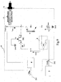
- a control circuit for a power transistor for example an IGBT transistor, which has been advantageously modified according to the invention with respect to the known solution of figure 4 and by inserting a JFET transistor TR2 in place of the resistance Rf of figure 4, is shown with 20.
- the circuit 20 is particularly, but not exclusively, suitable for applications in the automotive field for the electronic ignition in endothermic engines.
- the JFET transistor TR2 is connected, by means of a conduction terminal D thereof, particularly a Drain terminal, to a first conduction terminal, particularly a collector terminal C, of the IGBT transistor TR 1.
- the JFET transistor TR2 is also connected, by means of another conduction terminal S, particularly a source terminal, to the control terminal, i.e. the gate terminal G1, of said IGBT transistor TR1.
- the control terminal, i.e. the gate terminal G2, of said transistor TR2 is directly connected to a voltage reference, for example a ground GND.
- said JFET transistor TR2 is inserted in said control circuit 20, integrated in the same structure of said IGBT transistor TR1, allowing a driver for said IGBT transistor to be realised, using a low voltage technology.
- figure 7 schematically shows a sectional and enlarged-scale view of a structure of semiconductor-integrated electronic circuit 30 to realise in an integrated way the JFET transistor TR2 in the structure of said IGBT transistor TR1.
- Said structure 30 comprises a silicon substrate 32 having a first conductivity type N and associated to a metal electrode 31, as well as a plurality of silicon wells 33, 34 having a second conductivity type P, realised above said substrate 32.
- the well 33 is the body region of said JFET transistor TR2, while the well 34 is the active area of the JFET transistor.
- the structure 30 is covered by an oxide layer 35 with contact openings 36, 37 and 38 in correspondence with the wells 33 and 34.
- Metal layer ends 39 are overlapped to said layer 35 and in contact with said layer 32 through said opening 37, as well as with said well 33 through the opening 36 and with said well 34 through the opening 38.
- Figure 7 also shows, overlapped, the circuit equivalents of said layer 32 and of said JFET transistor TR2 represented by a resistance Re and a resistance Rj respectively.
- Figure 8 shows the typical curves of the circuit being implemented by the structure of figure 7.
- said JFET transistor TR2 is always conducting for a gate voltage equal to zero Volt and the current I JFET thereof decreases reverse-biasing the gate source junction, up to the pinch-off voltage value, equal to about -4V, for which said JFET transistor TR2 is completely inhibited.
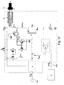
- the circuit of figure 9 in order to feedback the collector voltage, can be modified as in figure 10, wherein components and signals being already in figure 9 will keep the same labels as in figure 9.
- a block A located in the box, has been inserted in figure 10, through which the source terminal S of said JFET transistor TR2 is not directly connected to the gate G1 of the IGBT transistor TR1, but to the collector terminal of a first diode-connected bipolar transistor Q 1 of the NPN type, having the emitter terminal connected to the ground and being also connected through its base to the base terminal of a second bipolar transistor Q2 of the NPN type used as current mirror.
- this voltage is almost constant, and thus said second JFET transistor TR2 is forced to operate on a predetermined output feature, allowing a constant resistance value to be obtained in the ohmic area.
- the collector terminal of said second bipolar transistor Q2 of the NPN type is connected to the collector terminal of a third bipolar transistor Q3 of the PNP type, being connected in turn, in a current mirror configuration, to a forth bipolar transistor Q4 of the PNP type.
- the pairs of transistors Q1, Q2 and Q3, Q4 are substantially two current mirrors.
- the collector current I MIRR outputted by said forth bipolar transistor Q4 will then be equal to said current I JFET supplied by said JFET transistor TR2.
- Figure 11a shows the results of the simulation of the circuit of figure 9 and figure 11b shows those related to the circuit of figure 10.
- Figure 11b relates to the simulation of the same circuit wherein the block A of figure 10 has been introduced.
- the voltage calculated on the gate terminal G1 of said IGBT transistor TR1 reaches about 4V, but said JFET transistor TR2 is not inhibited, since it always detects between the source terminal S and the gate terminal G2 a voltage being equal to the voltage calculated between the base and emitter terminals of said first bipolar transistor Q 1 of the NPN type.
- the current I MIRR obtained by mirroring the current I JFET calculated in the source terminal S of the JFET transistor TR2, being not void, thus allows the feedback from the collector voltage required for the circuit stabilisation to be obtained.
- This feedback is also used to reduce the collector voltage overshoot occurring at the beginning of the current limitation step, when said IGBT transistor TR1 passes from the ohmic operation area thereof to the saturation area.
- a remarkable advantage of the JFET structure integrated inside an IGBT transistor is that of providing, with circuits realised by using low voltage technologies, all those circuit solutions previously requiring the use of high voltage technologies.
- the proposed solution provides that the feedback from the IGBT transistor collector voltage is obtained by realising an interface locating in the same IGBT transistor structure the high voltage area, in order to obtain a low voltage signal which can be operated by means of circuits which can be realised in any of the low voltage technologies.
- the proposed solution provides the realisation of an interface being capable to modify the feedback signal of the collector voltage, coming from the JFET transistor structure, to make it suitable for driving the IGBT transistor gate terminal G1.
- This circuit forces the JFET transistor to operate at a constant voltage (Vgs) calculated between the gate terminal and the source terminal, so that said transistor can be used on a predetermined output feature.
- Figure 5 shows an example of a possible exploitation of the ViPower technology to realise a control circuit for said IGBT transistor TR1, globally indicated with 18 in the figure, using said resistance Rf, globally indicated with 8 in the figure.
- the integrated structure 8 is effective to implement, with the ViPower technology, a high voltage resistance.
- the resistive structure 8 is integrated on a first semiconductor epitaxial layer 10 of a first conductivity type N, slightly doped (N-), located on a semiconductor substrate 9 of said first heavily doped conductivity type (N+); the resistive structure 8 comprised a plurality of buried and parallel regions 12, of a second conductivity type P, realised in the epitaxial layer 10.
- the resistive structure 8 also comprises two opposite end regions 13, always having said second heavily doped conductivity type (P+), in contact with the two buried end regions 12. At least a region 13 is laterally separated from a region 15 having a first heavily doped conductivity type (N+) by means of a portion 14 of the epitaxial layer 10.
- Said high voltage resistance being shown is capable to "throttle", considerably increasing the resistivity thereof, when the voltage at the ends exceeds a certain value, as shown in detail in the diagram of figure 6.
- the solution can be obtained by using also other high voltage technologies allowing a pinched resistance to be integrated.
- the IGBT transistor 18 comprises a semiconductor substrate 16 of said second heavily doped conductivity type (P ++ ), realising the bipolar transistor conduction electrodes, a region 21 of said second heavily doped conductivity type (P + ), called body region, realised in the first epitaxial layer 19 of said first slightly doped conductivity type (N-), while the driving terminal is realised in contact with the first epitaxial layer 19 itself.
- the vertical MOS transistor comprises said body region 21 wherein a source region 23 of said first heavily doped conductivity type (N + ), is integrated.
- a gate region 24 completes the IGBT transistor 18; a side portion of the region 21, wherein the source region 23 is integrated, can be used as body region 21b for the IGBT transistor.
- the resistance 8 is connected to the collector of the transistor 18 by placing the respective substrates 9 and 16 of the two dies on the same package frame 17, while the connection to the gate 24 of the transistor 18 is performed by means of an inner connection wire 25.
Landscapes
- Engineering & Computer Science (AREA)
- Chemical & Material Sciences (AREA)
- Combustion & Propulsion (AREA)
- Mechanical Engineering (AREA)
- General Engineering & Computer Science (AREA)
- Electronic Switches (AREA)
- Metal-Oxide And Bipolar Metal-Oxide Semiconductor Integrated Circuits (AREA)
Claims (8)
- Schaltung (20) für die dynamische Steuerung eines Leistungstransistors bei Anwendungen mit hoher Spannung, und zwar des Typs, bei dem ein Leistungstransistor (TR1) einen mit einer Last verbundenen Leitungsanschluss (C) sowie einen Steueranschluss (G1) aufweist, der ein Ansteuersignal von einem Treiberblock (4) erhält, der durch ein Auslösesignal (Vin) aktiviert wird, das an einem Schaltungseingangsanschluss (IN1) empfangen wird,
dadurch gekennzeichnet, dass sie eine JFET-Komponente (TR2) aufweist, die zwischen dem Leitungsanschluss (C) und dem Steueranschluss (G1) des Leistungstransistors (TR1) eingefügt ist und gleich einem Widerstand mit nichtlinearer Eigenschaft ist, wobei es sich bei der JFET-Komponente (TR2) um einen Transistor mit einem jeweiligen Drain-Anschluss (D) und Source-Anschluss (S) handelt, die mit dem Leitungsanschluss (C) und dem Steueranschluss (G1) des Leistungstransistors verbunden sind, sowie ferner einen Gateanschluss (G2) aufweist, der mit einer Referenzspannung (GND) direkt verbunden ist. - Schaltung nach Anspruch 1,
dadurch gekennzeichnet, dass die JFET-Komponente (TR2) in die Struktur des Leistungstransistors (TR1) monolithisch integriert ist. - Schaltung nach Anspruch 1,
dadurch gekennzeichnet, dass die JFET-Komponente (TR2) ein Rückkopplungswiderstand für den Leitungsanschluss des Leistungstransistors (TR1) ist. - Schaltung nach Anspruch 1,
dadurch gekennzeichnet, dass die JFET-Komponente (TR2) zwangsweise mit einer vorbestimmten Ausgangseigenschaft in dem ohmschen Bereich mit einem konstanten Widerstandswert betrieben wird. - Schaltung nach Anspruch 1,
dadurch gekennzeichnet, dass der JFET-Transistor (TR2) einer Schaltung (A) zugeordnet ist, die den Spannungsabfall zwischen dem Gateanschluss (G2) und dem Source-Anschluss (S) des JFET-Transistors einstellt, um diesen niedriger zu halten als eine Abschnürspannung. - Schaltung nach Anspruch 5,
dadurch gekennzeichnet, dass die Schaltung (A) zwischen dem Source-Anschluss (S) des JFET-Transistors (TR2) und dem Steueranschluss (G1) des Leistungstransistors (TR1) eingefügt ist und ein Paar Stromspiegel aufweist, um für eine Zufuhr des gleichen Stroms des JFET-Transistors zu sorgen. - Schaltung nach Anspruch 5,
dadurch gekennzeichnet, dass die Schaltung (A) eine Rückkopplungsverbindung an dem Leitungsanschluss (C) des Leistungstransistors (TR1) realisiert, die unabhängig von dem Spannungswert an dem Steueranschluss (G1) des gleichen Leistungstransistors (TR1) ist. - Schaltung nach Anspruch 1,
dadurch gekennzeichnet, dass die JFET-Komponente (TR2) mit einem konstanten Spannungsabfall (Vgs) arbeitet.
Priority Applications (3)
| Application Number | Priority Date | Filing Date | Title |
|---|---|---|---|
| DE602004009524T DE602004009524T2 (de) | 2004-01-22 | 2004-01-22 | Dynamische Steuerung eines Leistungstransistors bei Hochspannungsanwendungen |
| EP04425035A EP1557560B1 (de) | 2004-01-22 | 2004-01-22 | Dynamische Steuerung eines Leistungstransistors bei Hochspannungsanwendungen |
| US11/042,469 US20050184793A1 (en) | 2004-01-22 | 2005-01-24 | Circuit for dynamic control of a power transistor in applications for high voltage |
Applications Claiming Priority (1)
| Application Number | Priority Date | Filing Date | Title |
|---|---|---|---|
| EP04425035A EP1557560B1 (de) | 2004-01-22 | 2004-01-22 | Dynamische Steuerung eines Leistungstransistors bei Hochspannungsanwendungen |
Publications (2)
| Publication Number | Publication Date |
|---|---|
| EP1557560A1 EP1557560A1 (de) | 2005-07-27 |
| EP1557560B1 true EP1557560B1 (de) | 2007-10-17 |
Family
ID=34626570
Family Applications (1)
| Application Number | Title | Priority Date | Filing Date |
|---|---|---|---|
| EP04425035A Expired - Lifetime EP1557560B1 (de) | 2004-01-22 | 2004-01-22 | Dynamische Steuerung eines Leistungstransistors bei Hochspannungsanwendungen |
Country Status (3)
| Country | Link |
|---|---|
| US (1) | US20050184793A1 (de) |
| EP (1) | EP1557560B1 (de) |
| DE (1) | DE602004009524T2 (de) |
Families Citing this family (3)
| Publication number | Priority date | Publication date | Assignee | Title |
|---|---|---|---|---|
| FR2949630B1 (fr) * | 2009-08-31 | 2019-04-05 | Safran Electrical & Power | Module electronique de commande pour transistor jfet |
| WO2015070347A1 (en) * | 2013-11-14 | 2015-05-21 | Tm4 Inc. | Commutation cell, power converter and compensation circuit having dynamically controlled voltage gains |
| US11131286B2 (en) * | 2018-03-20 | 2021-09-28 | Rohm Co., Ltd. | Igniter and vehicle provided with the same |
Family Cites Families (8)
| Publication number | Priority date | Publication date | Assignee | Title |
|---|---|---|---|---|
| EP0730347A3 (de) * | 1992-03-18 | 1996-10-23 | Fuji Electric Co Ltd | Halbleitervorrichtung |
| US5477175A (en) * | 1993-10-25 | 1995-12-19 | Motorola | Off-line bootstrap startup circuit |
| JP3477852B2 (ja) * | 1994-11-04 | 2003-12-10 | 株式会社デンソー | Igbt駆動回路および点火装置 |
| JP3373704B2 (ja) * | 1995-08-25 | 2003-02-04 | 三菱電機株式会社 | 絶縁ゲートトランジスタ駆動回路 |
| EP0814564A1 (de) * | 1996-06-20 | 1997-12-29 | ANSALDO INDUSTRIA S.p.A. | Elektronischer Schaltkreis mit reduzierten Schalttransienten |
| JP3530714B2 (ja) * | 1997-05-26 | 2004-05-24 | 株式会社日立製作所 | 内燃機関用点火装置 |
| JP3482161B2 (ja) * | 1999-08-03 | 2003-12-22 | 株式会社日立製作所 | 内燃機関の点火システム |
| US6563724B2 (en) * | 2001-10-03 | 2003-05-13 | Bruce W. Carsten | Apparatus and method for turning off BJT used as synchronous rectifier |
-
2004
- 2004-01-22 DE DE602004009524T patent/DE602004009524T2/de not_active Expired - Fee Related
- 2004-01-22 EP EP04425035A patent/EP1557560B1/de not_active Expired - Lifetime
-
2005
- 2005-01-24 US US11/042,469 patent/US20050184793A1/en not_active Abandoned
Also Published As
| Publication number | Publication date |
|---|---|
| EP1557560A1 (de) | 2005-07-27 |
| DE602004009524T2 (de) | 2008-07-31 |
| US20050184793A1 (en) | 2005-08-25 |
| DE602004009524D1 (de) | 2007-11-29 |
Similar Documents
| Publication | Publication Date | Title |
|---|---|---|
| US6194884B1 (en) | Circuitry for maintaining a substantially constant sense current to load current ratio through an electrical load driving device | |
| US5723916A (en) | Electrical load driving device including load current limiting circuitry | |
| US10879894B2 (en) | Driver circuit, corresponding device and method | |
| US6100728A (en) | Coil current limiting feature for an ignition coil driver module | |
| US5576648A (en) | Temperature stable circuit for controlled current discharge during the driving of an inductive load | |
| JPH08293774A (ja) | ゲート駆動回路 | |
| US7190207B2 (en) | One way conductor | |
| JP3979096B2 (ja) | 半導体素子の駆動装置ならびにそれを用いた電力変換装置 | |
| KR0177145B1 (ko) | 전력 fet용 적응 게이트 충전 회로 | |
| AU641491B2 (en) | Current limiter circuit | |
| JPH07273608A (ja) | フリップ・フロップ回路 | |
| EP1557560A1 (de) | Dynamische Steuerung eines Leistungstransistors bei Hochspannungsanwendungen | |
| JP2002157027A (ja) | 電力変換装置及び半導体装置 | |
| US7368784B2 (en) | Thermal protection device for an integrated power MOS | |
| JP2003078361A (ja) | 電源回路及び半導体装置 | |
| JP4590888B2 (ja) | 半導体出力回路 | |
| EP0757441B1 (de) | Integrierte Schaltung zur Spannungsbegrenzung | |
| JPH0743276U (ja) | 電子機器の保護回路 | |
| US7159583B2 (en) | Technique for drive current stabilization of an automotive ignition system | |
| JPH11234108A (ja) | 誘導負荷をスイッチングするためのスイッチング装置 | |
| JP2004088192A (ja) | 電圧駆動素子の駆動回路 | |
| US20040255920A1 (en) | Multichannel electronic ignition device with high-voltage controller | |
| JP3019039B2 (ja) | 内燃機関点火装置 | |
| JP3570338B2 (ja) | 電源逆接続保護回路 | |
| EP1727203A1 (de) | Monolithisch integrierte Leistungs-IGBT Vorrichtung (Bipolartransistor mit isolierter Gate-Elektrode) |
Legal Events
| Date | Code | Title | Description |
|---|---|---|---|
| PUAI | Public reference made under article 153(3) epc to a published international application that has entered the european phase |
Free format text: ORIGINAL CODE: 0009012 |
|
| AK | Designated contracting states |
Kind code of ref document: A1 Designated state(s): AT BE BG CH CY CZ DE DK EE ES FI FR GB GR HU IE IT LI LU MC NL PT RO SE SI SK TR |
|
| AX | Request for extension of the european patent |
Extension state: AL LT LV MK |
|
| 17P | Request for examination filed |
Effective date: 20060118 |
|
| AKX | Designation fees paid |
Designated state(s): DE FR GB IT |
|
| 17Q | First examination report despatched |
Effective date: 20060703 |
|
| GRAP | Despatch of communication of intention to grant a patent |
Free format text: ORIGINAL CODE: EPIDOSNIGR1 |
|
| GRAS | Grant fee paid |
Free format text: ORIGINAL CODE: EPIDOSNIGR3 |
|
| GRAA | (expected) grant |
Free format text: ORIGINAL CODE: 0009210 |
|
| AK | Designated contracting states |
Kind code of ref document: B1 Designated state(s): DE FR GB IT |
|
| REG | Reference to a national code |
Ref country code: GB Ref legal event code: FG4D |
|
| REF | Corresponds to: |
Ref document number: 602004009524 Country of ref document: DE Date of ref document: 20071129 Kind code of ref document: P |
|
| PGFP | Annual fee paid to national office [announced via postgrant information from national office to epo] |
Ref country code: IT Payment date: 20080122 Year of fee payment: 5 Ref country code: DE Payment date: 20080115 Year of fee payment: 5 |
|
| EN | Fr: translation not filed | ||
| PLBE | No opposition filed within time limit |
Free format text: ORIGINAL CODE: 0009261 |
|
| STAA | Information on the status of an ep patent application or granted ep patent |
Free format text: STATUS: NO OPPOSITION FILED WITHIN TIME LIMIT |
|
| 26N | No opposition filed |
Effective date: 20080718 |
|
| GBPC | Gb: european patent ceased through non-payment of renewal fee |
Effective date: 20080122 |
|
| PG25 | Lapsed in a contracting state [announced via postgrant information from national office to epo] |
Ref country code: FR Free format text: LAPSE BECAUSE OF FAILURE TO SUBMIT A TRANSLATION OF THE DESCRIPTION OR TO PAY THE FEE WITHIN THE PRESCRIBED TIME-LIMIT Effective date: 20080801 |
|
| PG25 | Lapsed in a contracting state [announced via postgrant information from national office to epo] |
Ref country code: GB Free format text: LAPSE BECAUSE OF NON-PAYMENT OF DUE FEES Effective date: 20080122 |
|
| PG25 | Lapsed in a contracting state [announced via postgrant information from national office to epo] |
Ref country code: DE Free format text: LAPSE BECAUSE OF NON-PAYMENT OF DUE FEES Effective date: 20090801 |
|
| PG25 | Lapsed in a contracting state [announced via postgrant information from national office to epo] |
Ref country code: IT Free format text: LAPSE BECAUSE OF NON-PAYMENT OF DUE FEES Effective date: 20090122 |