EP1557719A2 - Réserve chimiquement amplifiée et procédé de formation de motifs - Google Patents
Réserve chimiquement amplifiée et procédé de formation de motifs Download PDFInfo
- Publication number
- EP1557719A2 EP1557719A2 EP05001274A EP05001274A EP1557719A2 EP 1557719 A2 EP1557719 A2 EP 1557719A2 EP 05001274 A EP05001274 A EP 05001274A EP 05001274 A EP05001274 A EP 05001274A EP 1557719 A2 EP1557719 A2 EP 1557719A2
- Authority
- EP
- European Patent Office
- Prior art keywords
- water
- resist
- film
- chemically amplified
- formation method
- Prior art date
- Legal status (The legal status is an assumption and is not a legal conclusion. Google has not performed a legal analysis and makes no representation as to the accuracy of the status listed.)
- Withdrawn
Links
Images


Classifications
-
- G—PHYSICS
- G03—PHOTOGRAPHY; CINEMATOGRAPHY; ANALOGOUS TECHNIQUES USING WAVES OTHER THAN OPTICAL WAVES; ELECTROGRAPHY; HOLOGRAPHY
- G03F—PHOTOMECHANICAL PRODUCTION OF TEXTURED OR PATTERNED SURFACES, e.g. FOR PRINTING, FOR PROCESSING OF SEMICONDUCTOR DEVICES; MATERIALS THEREFOR; ORIGINALS THEREFOR; APPARATUS SPECIALLY ADAPTED THEREFOR
- G03F7/00—Photomechanical, e.g. photolithographic, production of textured or patterned surfaces, e.g. printing surfaces; Materials therefor, e.g. comprising photoresists; Apparatus specially adapted therefor
- G03F7/004—Photosensitive materials
- G03F7/039—Macromolecular compounds which are photodegradable, e.g. positive electron resists
- G03F7/0392—Macromolecular compounds which are photodegradable, e.g. positive electron resists the macromolecular compound being present in a chemically amplified positive photoresist composition
-
- G—PHYSICS
- G03—PHOTOGRAPHY; CINEMATOGRAPHY; ANALOGOUS TECHNIQUES USING WAVES OTHER THAN OPTICAL WAVES; ELECTROGRAPHY; HOLOGRAPHY
- G03F—PHOTOMECHANICAL PRODUCTION OF TEXTURED OR PATTERNED SURFACES, e.g. FOR PRINTING, FOR PROCESSING OF SEMICONDUCTOR DEVICES; MATERIALS THEREFOR; ORIGINALS THEREFOR; APPARATUS SPECIALLY ADAPTED THEREFOR
- G03F7/00—Photomechanical, e.g. photolithographic, production of textured or patterned surfaces, e.g. printing surfaces; Materials therefor, e.g. comprising photoresists; Apparatus specially adapted therefor
- G03F7/004—Photosensitive materials
- G03F7/09—Photosensitive materials characterised by structural details, e.g. supports, auxiliary layers
- G03F7/11—Photosensitive materials characterised by structural details, e.g. supports, auxiliary layers having cover layers or intermediate layers, e.g. subbing layers
-
- G—PHYSICS
- G03—PHOTOGRAPHY; CINEMATOGRAPHY; ANALOGOUS TECHNIQUES USING WAVES OTHER THAN OPTICAL WAVES; ELECTROGRAPHY; HOLOGRAPHY
- G03F—PHOTOMECHANICAL PRODUCTION OF TEXTURED OR PATTERNED SURFACES, e.g. FOR PRINTING, FOR PROCESSING OF SEMICONDUCTOR DEVICES; MATERIALS THEREFOR; ORIGINALS THEREFOR; APPARATUS SPECIALLY ADAPTED THEREFOR
- G03F7/00—Photomechanical, e.g. photolithographic, production of textured or patterned surfaces, e.g. printing surfaces; Materials therefor, e.g. comprising photoresists; Apparatus specially adapted therefor
- G03F7/20—Exposure; Apparatus therefor
- G03F7/2041—Exposure; Apparatus therefor in the presence of a fluid, e.g. immersion; using fluid cooling means
-
- G—PHYSICS
- G03—PHOTOGRAPHY; CINEMATOGRAPHY; ANALOGOUS TECHNIQUES USING WAVES OTHER THAN OPTICAL WAVES; ELECTROGRAPHY; HOLOGRAPHY
- G03F—PHOTOMECHANICAL PRODUCTION OF TEXTURED OR PATTERNED SURFACES, e.g. FOR PRINTING, FOR PROCESSING OF SEMICONDUCTOR DEVICES; MATERIALS THEREFOR; ORIGINALS THEREFOR; APPARATUS SPECIALLY ADAPTED THEREFOR
- G03F7/00—Photomechanical, e.g. photolithographic, production of textured or patterned surfaces, e.g. printing surfaces; Materials therefor, e.g. comprising photoresists; Apparatus specially adapted therefor
- G03F7/004—Photosensitive materials
- G03F7/0046—Photosensitive materials with perfluoro compounds, e.g. for dry lithography
Definitions
- the present invention relates to a chemically amplified resist used in pattern formation in fabrication process or the like for semiconductor devices and a pattern formation method using the same.
- Pattern formation is currently carried out through photolithography using exposing light of a mercury lamp, KrF excimer laser, ArF excimer laser or the like. Also, in order to form a fine pattern with exposing light of a wavelength of 0.1 ⁇ m or less, and more particularly, of 70 nm or less, examinations are being made on application of a shorter wavelength, such as vacuum UV like F 2 laser of a wavelength of a 157 nm band or extreme UV of a wavelength of a 1 nm through 30 nm band. Furthermore, application of electron beams of electron beam (EB) projection exposure is being examined.
- EB electron beams of electron beam
- the vacuum UV such as F 2 laser or the electron beam
- a gas outgassed in the exposure is adhered onto a lens, mirror or the like included in an exposure system or a mask, and hence, it is apprehended that the illuminance is lowered, the accuracy of a desired pattern is degraded or the throughput is lowered (see, for example, S. Hien et al., "Photoresist Outgassing at 157 nm Exposure", Proc. SPIE, Vol. 4345, p. 439 (2001)).
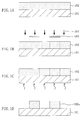
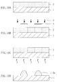
- FIGS. 10A through 10D a conventional pattern formation method using F 2 laser as the exposing light will be described with reference to FIGS. 10A through 10D .
- the aforementioned chemically amplified resist material is applied on a substrate 1 so as to form a resist film 2 with a thickness of 0.15 ⁇ m.
- pattern exposure is carried out by irradiating the resist film 2 with exposing light 3 of F 2 laser with numerical aperture (NA) of 0.85 through a mask 4.
- NA numerical aperture
- the resist film 2 is baked with a hot plate at a temperature of 110°C for 60 seconds (post exposure bake).
- the resultant resist film 2 is developed with a 2.38 wt% tetramethylammonium hydroxide aqueous solution (alkaline developer). In this manner, a resist pattern 2a made of an unexposed portion of the resist film 2 and having a line width of 0.08 ⁇ m is formed as shown in FIG. 10D .
- the resist pattern 2a formed by the conventional pattern formation method is in a defective shape. This pattern failure seems to be caused because of outgassing from the resist film 2 made of the chemically amplified resist irradiated with the exposing light and the thus generated gas is adhered onto a lens and the like.
- a gas generated from the resist is mainly derived from vaporization of an acid labile group included in the chemically amplified resist.
- a gas is outgassed from the resist film 2 made of a chemically amplified resist irradiated with the exposing light in the exposure, and the thus generated gas forms foams within the liquid 5 .
- foams formed in the liquid 5 causes, for example, diffraction of the exposing light 3 , and hence, the resultant pattern is in a defective shape.
- the resultant pattern of the target film is also in a defective shape, resulting in disadvantageously lowering the productivity and the yield in the fabrication process of semiconductor devices.
- an object of the invention is forming a fine pattern in a good shape by preventing a gas outgassed from a resist through irradiation with exposing light from reaching members provided in an exposure system.
- the present inventors have made various examinations for preventing outgassing from a resist through irradiation with exposing light, resulting in finding the following:
- a water-soluble polymer with lower gas permeability than a chemically amplified resist is included in the chemically amplified resist or is deposited on the chemically amplified resist, the trouble caused in members of an exposure system such as a lens and a liquid by outgassing from a resist irradiated with exposing light can be prevented.
- a gas outgassed from a resist film can be prevented from reaching a lens or a liquid by including, in a chemically amplified resist, a water-soluble polymer with lower gas permeability than the chemically amplified resist or by forming a film of the water-soluble polymer on the resist film.
- the present invention is practiced as follows:
- the chemically amplified resist of this invention includes a water-soluble polymer having lower gas permeability than the chemically amplified resist excluding the water-soluble polymer.
- the chemically amplified resist of this invention includes the water-soluble polymer having lower gas permeability than the chemically amplified resist excluding the water-soluble polymer, even when outgassing is caused in the chemically amplified resist through irradiation with exposing light, the thus generated gas minimally permeates the water-soluble polymer within the resist and hence is substantially captured by the water-soluble polymer. Accordingly, the gas outgassed from the chemically amplified resist minimally reaches optical members such as a lens of an exposure system and a mask, so as to avoid the trouble of the exposure system and the mask. As a result, a fine pattern can be formed in a good shape.
- the content of the water-soluble polymer in the chemically amplified resist may be approximately 0.1 wt% through 10 wt% for attaining a sufficient effect, but the content is not limited to this range but may be increased/reduced depending upon the compositions of the chemically amplified resist and the water-soluble polymer.
- the first pattern formation method of this invention includes the steps of forming, on a substrate, a resist film made of a chemically amplified resist including a water-soluble polymer; performing pattern exposure by selectively irradiating the resist film with exposing light; and forming a resist pattern made of the resist film by developing the resist film after the pattern exposure, and the water-soluble film has lower gas permeability than the chemically amplified resist excluding the water-soluble polymer.
- the thus generated gas minimally permeates the water-soluble polymer within the resist and hence is substantially captured by the water-soluble polymer. Accordingly, the gas outgassed from the chemically amplified resist minimally reaches optical members such as a lens of an exposure system and a mask, and hence the trouble of the exposure system and the mask can be avoided. As a result, a fine resist pattern can be formed in a good shape.
- the second pattern formation method of this invention includes the steps of forming, on a substrate, a resist film made of a chemically amplified resist; forming, on the resist film, a water-soluble film containing a water-soluble polymer having lower gas permeability than the chemically amplified resist; performing pattern exposure by selectively irradiating the resist film with exposing light through the water-soluble film; and forming a resist pattern made of the resist film by developing the resist film after removing the water-soluble film after the pattern exposure.
- the thus generated gas minimally permeates the water-soluble film containing the water-soluble polymer formed on the resist film and hence is substantially captured by the water-soluble film. Accordingly, the gas outgassed from the chemically amplified resist minimally reaches optical members such as a lens of an exposure system and a mask, and hence the trouble of the exposure system and the mask can be avoided. As a result, a fine resist pattern can be formed in a good shape.
- the third pattern formation method of this invention includes the steps of forming, on a substrate, a resist film made of a chemically amplified resist; forming, on the resist film, a water-soluble film containing a water-soluble polymer having lower gas permeability than the chemically amplified resist; performing pattern exposure by selectively irradiating the resist film with exposing light through the water-soluble film; and removing the water-soluble film and forming a resist pattern made of the resist film by developing the resist film after the pattern exposure.
- the thus generated gas minimally permeates the water-soluble film made of the water-soluble polymer formed on the resist film and hence is substantially captured by the water-soluble film. Accordingly, the gas outgassed from the chemically amplified resist minimally reaches optical members such as a lens of an exposure system and a mask, and hence the trouble of the exposure system and the mask can be avoided. As a result, a fine resist pattern can be formed in a good shape.
- the water-soluble film formed on the resist film is removed before the development in the second pattern formation method while it is removed during the development in the third pattern formation method.
- the second pattern formation method since the water-soluble film is removed before the development, the development is proceeded in a general manner.
- the dissolving characteristic of the resist can be controlled, resulting in improving the dissolving characteristic of the resist. The control of the dissolving characteristic will be described later.
- the exposing light may be KrF excimer laser, ArF excimer laser, F 2 laser, ArKr laser, Ar 2 laser, extreme UV of a wavelength band not shorter than 1. nm and not longer than 30 nm, or electron beams.
- the fourth pattern formation method of this invention includes the steps of forming, on a substrate, a resist film made of a chemically amplified resist including a water-soluble polymer; performing pattern exposure by selectively irradiating the resist film with exposing light with a liquid provided on the resist film; and forming a resist pattern made of the resist film by developing the resist film after the pattern exposure, and the water-soluble polymer has lower gas permeability than the chemically amplified resist excluding the water-soluble polymer.
- the thus generated gas minimally permeates the water-soluble polymer within the resist film and hence is substantially captured by the water-soluble polymer. Accordingly, the gas outgassed from the chemically amplified resist minimally reaches the liquid, and hence foams derived from outgassing are not formed. Thus, the exposing light is not affected by the foams, and as a result, a fine resist pattern can be formed in a good shape.
- the content of the water-soluble polymer in the chemically amplified resist is approximately 0.1 wt% through 10wt% for attaining a sufficient effect, but the content is not limited to this range but may be increased/reduced depending upon the composition of the chemically amplified resist or the water-soluble polymer.
- the fifth pattern formation method of this invention includes the steps of forming, on a substrate, a resist film made of a chemically amplified resist; forming, on the resist film, a water-soluble film containing a water-soluble polymer having lower gas permeability than the chemically amplified resist; performing pattern exposure by selectively irradiating the resist film with exposing light through the water-soluble film with a liquid provided on the water-soluble film; and forming a resist pattern made of the resist film by developing the resist film after removing the water-soluble film after the pattern exposure.
- the thus generated gas minimally permeates the water-soluble film made of the water-soluble polymer formed on the resist film and hence is substantially captured by the water-soluble film. Accordingly, the gas outgassed from the chemically amplified resist minimally reaches the liquid, and hence foams derived from outgassing are not formed. Thus, the exposing light is not affected by the foams, and as a result, a fine resist pattern can be formed in a good shape.
- the sixth pattern formation method of this invention includes the steps of forming, on a substrate, a resist film made of a chemically amplified resist; forming, on the resist film, a water-soluble film containing a water-soluble polymer having lower gas permeability than the chemically amplified resist; performing pattern exposure by selectively irradiating the resist film with exposing light through the water-soluble film with a liquid provided on the water-soluble film; and removing the water-soluble film and forming a resist pattern made of the resist film by developing the resist film after the pattern exposure.
- the thus generated gas minimally permeates the water-soluble film made of the water-soluble polymer formed on the resist film and hence is substantially captured by the water-soluble film. Accordingly, the gas outgassed from the chemically amplified resist minimally reaches the liquid, and hence foams derived from outgassing are not formed. Thus, the exposing light is not affected by the foams, and as a result, a fine resist pattern can be formed in a good shape.
- the water-soluble film formed on the resist film is removed before the development in the fifth pattern formation method while it is removed during the development in the sixth pattern formation method.
- the development is proceeded in a general manner.
- the dissolving characteristic of the resist can be controlled, resulting in improving the dissolving characteristic of the resist. The control of the dissolving characteristic will be described later.
- the liquid may be water or perfluoropolyether.
- the liquid may be a non-aqueous solution such as perfluoropolyether.
- the exposing light may be KrF excimer laser, ArF excimer laser, F 2 laser, ArKr laser or Ar 2 laser.
- the chemically amplified resist preferably includes a water-soluble polymer having lower gas permeability than the chemically amplified resist excluding the water-soluble polymer.
- the gas outgassed from the chemically amplified resist during the exposure can be more effectively prevented from reaching the members of the exposing system, the mask or the liquid.
- the water-soluble polymer may be at least one of polyacrylic acid, polystyrenesulfonic acid, hydroxyethyl cellulose, polyisoprenesulfonic acid, polyvinyl pyrrolidone and pullulan.
- FIGS. 1A through 1D A pattern formation method using a water-soluble material according to Embodiment 1 of the invention will now be described with reference to FIGS. 1A through 1D .
- the aforementioned chemically amplified resist material is applied on a substrate 101 so as to form a resist film 102 with a thickness of 0.15 ⁇ m.
- pattern exposure is carried out by irradiating the resist film 102 with exposing light 104 of F 2 laser with numerical aperture (NA) of 0.85 through a mask 103.
- NA numerical aperture
- the resist film 102 is baked with a hot plate at a temperature of 110°C for 60 seconds (post exposure bake).
- the resultant resist film 102 is developed with a 2.38 wt% tetramethylammonium hydroxide aqueous solution (alkaline developer). In this manner, a resist pattern 102a made of an unexposed portion of the resist film 102 and having a line width of 0.08 ⁇ m is formed in a good shape as shown in FIG. 1D .
- the resist material for the resist film 102 includes polyvinyl pyrrolidone with lower gas permeability than the chemically amplified resist excluding the water-soluble polymer (i.e., polyvinyl pyrrolidone). Therefore, in the step of pattern exposure shown in FIG. 1B , outgassing from the resist film 102 is reduced to an undetectable level. Accordingly, a gas is not adhered onto a lens and a mirror included in an exposure system (not shown), the mask 103 and the like, resulting in forming the fine resist pattern 102a in a good shape.
- the water-soluble polymer included in the chemically amplified resist is not limited to polyvinyl pyrrolidone but at least one of polyvinyl pyrrolidone, polyacrylic acid, polystyrenesulfonic acid, hydroxyethyl cellulose, polyisoprenesulfonic acid and pullulan may be used.
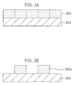
- a pattern formation method using a water-soluble material according to Embodiment 2 of the invention will now be described with reference to FIGS. 2A through 2D, 3A and 3B .
- the aforementioned chemically amplified resist material is applied on a substrate 201 so as to form a resist film 202 with a thickness of 0.15 ⁇ m.
- a water-soluble film 203 with a thickness of 0.05 ⁇ m that is made of a water-soluble material having the following composition and has lower gas permeability than the resist film 202 is formed on the resist film 202 by, for example, spin coating:
- pattern exposure is carried out by irradiating, through the water-soluble film 203, the resist film 202 with exposing light 205 of F 2 laser with NA of 0.85 having passed through a mask 204.
- the resist film 202 is baked with a hot plate at a temperature of 110°C for 60 seconds (post exposure bake).
- the resultant resist film 202 is developed with a 2.38 wt% tetramethylammonium hydroxide aqueous solution (alkaline developer). In this manner, a resist pattern 202a made of an unexposed portion of the resist film 202 and having a line width of 0.08 ⁇ m is formed in a good shape as shown in FIG. 3B.
- the water-soluble film 203 made of the water-soluble polymer (i.e., polyvinyl pyrrolidone) with lower gas permeability than the chemically amplified resist used for forming the resist film 202 is formed on the resist film 202 before the pattern exposure as shown in FIG. 2B. Therefore, in the step of pattern exposure shown in FIG. 2C , a gas outgassed from the resist film 202 is captured by the water-soluble film 203 . Accordingly, the gas is not adhered onto a lens and a mirror included in an exposure system (not shown), the mask 204 and the like, resulting in forming the fine resist pattern 202a in a good shape.
- the water-soluble film 203 made of the water-soluble polymer i.e., polyvinyl pyrrolidone
- the water-soluble polymer used for the water-soluble film 203 is not limited to polyvinyl pyrrolidone but at least one of polyvinyl pyrrolidone, polyacrylic acid, polystyrenesulfonic acid, hydroxyethyl cellulose, polyisoprenesulfonic acid and pullulan may be used.
- water-soluble polymers may be included in the resist material as in Embodiment 1.
- the aforementioned chemically amplified resist material is applied on a substrate 301 so as to form a resist film 302 with a thickness of 0.15 ⁇ m.
- a water-soluble film 303 with a thickness of 0.05 ⁇ m that is made of a water-soluble material having the following composition and has lower gas permeability than the resist film 302 is formed on the resist film 302 by, for example, the spin coating:
- pattern exposure is carried out by irradiating, through the water-soluble film 303, the resist film 302 with exposing light 305 of F 2 laser with NA of 0.85 having passed through a mask 304.
- the resist film 302 is baked with a hot plate at a temperature of 110°C for 60 seconds (post exposure bake).
- the water-soluble film 303 is removed and the resultant resist film 302 is developed with a 2.38 wt% tetramethylammonium hydroxide aqueous solution (alkaline developer).
- a resist pattern 302a made of an unexposed portion of the resist film 302 and having a line width of 0.08 ⁇ m is formed in a good shape as shown in FIG. 4E.
- the water-soluble film 303 made of the water-soluble polymer (i.e., hydroxyethyl cellulose) with lower gas permeability than the chemically amplified resist used for forming the resist film 302 is formed on the resist film 302 before the pattern exposure as shown in FIG. 4B. Therefore, in the step of pattern exposure shown in FIG. 4C, a gas outgassed from the resist film 302 is captured by the water-soluble film 303 . Accordingly, the gas is not adhered onto a lens and a mirror included in an exposure system (not shown), the mask 304 and the like, resulting in forming the fine resist pattern 302a in a good shape.
- the water-soluble polymer used for the water-soluble film 303 is not limited to hydroxyethyl cellulose but at least one of hydroxyethyl cellulose, polyacrylic acid, polystyrenesulfonic acid, polyisoprenesulfonic acid, polyvinyl pyrrolidone and pullulan may be used.
- water-soluble polymers may be included in the resist material as in Embodiment 1.
- F 2 laser is used as the exposing light in each of Embodiments 1 through 3
- KrF excimer laser, ArF excimer laser, ArKr laser, Ar 2 laser, extreme UV of a wavelength band not shorter than 1 nm and not longer than 30 nm or electron means may be used as the exposing light instead.
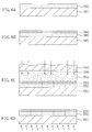
- a pattern formation method using a water-soluble material according to Embodiment 4 of the invention will now be described with reference to FIGS. 5A through 5D .
- the aforementioned chemically amplified resist material is applied on a substrate 401 so as to form a resist film 402 with a thickness of 0.35 ⁇ m.
- pattern exposure is carried out by irradiating the resist film 402 with exposing light 404 of ArF excimer laser with NA of 0.65 through a mask (not shown).
- the resist film 402 is baked with a hot plate at a temperature of 105°C for 60 seconds (post exposure bake).
- the resultant resist film 402 is developed with a 2.38 wt% tetramethylammonium hydroxide aqueous solution (alkaline developer). In this manner, a resist pattern 402a made of an unexposed portion of the resist film 402 and having a line width of 0.09 ⁇ m is formed in a good shape as shown in FIG. 5D.
- the resist material used for forming the resist film 402 includes polyvinyl pyrrolidone with lower gas permeability than the chemically amplified resist excluding the water-soluble polymer (i.e., polyvinyl pyrrolidone). Therefore, in the step of pattern exposure through the liquid 403 shown in FIG. 5B , a gas outgassed from the resist film 402 is captured in the resist film 402.
- foams derived from outgassing is not formed in the liquid 403 provided on the resist film 402 , and hence, the exposing light 404 is free from influence of the foams such as diffraction, resulting in forming the fine resist pattern 402a in a good shape.
- the water-soluble polymer included in the chemically amplified resist is not limited to polyvinyl pyrrolidone but at least one of polyvinyl pyrrolidone, polyacrylic acid, polystyrenesulfonic acid, hydroxyethyl cellulose, polyisoprenesulfonic acid and pullulan may be used.
- the immersion liquid 403 of water may include an appropriate amount of surface active agent.
- the liquid 403 is not limited to water by may be perfluoropolyether instead.
- FIGS. 6A through 6D, 7A and 7B A pattern formation method using a water-soluble material according to Embodiment 5 of the invention will now be described with reference to FIGS. 6A through 6D, 7A and 7B .
- the aforementioned chemically amplified resist material is applied on a substrate 501 so as to form a resist film 502 with a thickness of 0.15 ⁇ m.
- a water-soluble film 503 with a thickness of 0.05 ⁇ m that is made of a water-soluble material having the following composition and has lower gas permeability than the resist film 502 is formed on the resist film 502 by, for example, the spin coating:
- pattern exposure is carried out by irradiating the resist film 502 with exposing light 505 of F 2 laser with NA of 0.85 through a mask (not shown).
- the resist film 502 is baked with a hot plate at a temperature of 110°C for 60 seconds (post exposure bake).
- the resultant resist film 502 is developed with a 2.38 wt% tetramethylammonium hydroxide aqueous solution (alkaline developer). In this manner, a resist pattern 502a made of an unexposed portion of the resist film 502 and having a line width of 0.08 ⁇ m is formed in a good shape as shown in FIG. 7B .
- the water-soluble film 503 made of the water-soluble material (i.e., polyvinyl pyrrolidone) with lower gas permeability than the chemically amplified resist used for forming the resist film 502 is formed on the resist film 502 before the pattern exposure as shown in FIG. 6B . Therefore, in the step of pattern exposure through the liquid 504 shown in FIG. 6C, a gas outgassed from the resist film 502 is captured by the water-soluble film 503.
- the water-soluble film 503 made of the water-soluble material i.e., polyvinyl pyrrolidone
- foams derived from outgassing is not formed in the liquid 504 provided on the water-soluble film 503, and hence, the exposing light 505 is free from influence of the foams such as diffraction, resulting in forming the fine resist pattern 502a in a good shape.
- the water-soluble polymer included in the water-soluble film 503 is not limited to polyvinyl pyrrolidone but at least one of polyvinyl pyrrolidone, polyacrylic acid, polystyrenesulfonic acid, hydroxyethyl cellulose, polyisoprenesulfonic acid and pullulan may be used.
- At least one of the water-soluble polymers may be included in the resist material as in Embodiment 4.
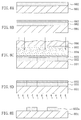
- FIGS. 8A through 8E A pattern formation method using a water-soluble material according to Embodiment 6 of the invention will now be described with reference to FIGS. 8A through 8E .
- the aforementioned chemically amplified resist material is applied on a substrate 601 so as to form a resist film 602 with a thickness of 0.15 ⁇ m.
- a water-soluble film 603 with a thickness of 0.06 ⁇ m that is made of a water-soluble material having the following composition and has lower gas permeability than the resist film 602 is formed on the resist film 602 by, for example, the spin coating:
- pattern exposure is carried out by irradiating the resist film 602 with exposing light 605 of F 2 laser with NA of 0.85 through a mask (not shown).
- the resist film 602 is baked with a hot plate at a temperature of 110°C for 60 seconds (post exposure bake).
- the water-soluble film 603 is removed and the resultant resist film 602 is developed with a 2.38 wt% tetramethylammonium hydroxide aqueous solution (alkaline developer).
- a resist pattern 602a made of an unexposed portion of the resist film 602 and having a line width of 0.08 ⁇ m is formed in a good shape as shown in FIG. 8E.
- the water-soluble film 603 made of the water-soluble material (i.e., hydroxyethyl cellulose) with lower gas permeability than the chemically amplified resist used for forming the resist film 602 is formed on the resist film 602 before the pattern exposure as shown in FIG. 8B. Therefore, in the step of pattern exposure through the liquid 604 shown in FIG. 8C, a gas outgassed from the resist film 602 is captured by the water-soluble film 603.
- the water-soluble film 603 made of the water-soluble material i.e., hydroxyethyl cellulose
- foams derived from outgassing is not formed in the liquid 604 provided on the water-soluble film 603 , and hence, the exposing light 605 is free from influence of the foams such as diffraction, resulting in forming the fine resist pattern 602a in a good shape.
- the water-soluble polymer included in the water-soluble film 603 is not limited to hydroxyethyl cellulose but at least one of hydroxyethyl cellulose, polyacrylic acid, polystyrenesulfonic acid, polyisoprenesulfonic acid, polyvinyl pyrrolidone and pullulan may be used.
- At least one of the water-soluble polymers may be included in the resist material as in Embodiment 4.
- Embodiments 3 and 6 the water-soluble films 303 and 603 are removed during the development, namely, with the developer, differently from Embodiments 2 and 5.
- the dissolving characteristic of the resist films 302 and 602 can be controlled. The control of the dissolving characteristic will now be described with reference to FIG. 9 .
- the dissolving rate is abruptly increased when exposure exceeds a given threshold value as shown with a graph A of a broken line in FIG. 9 .
- a difference in the solubility between an exposed portion and an unexposed portion of the resist film 302 or 602 is larger, and hence, higher resolution can be attained, namely, the resist pattern 302a or 602a can be formed in a better shape.
- the dissolving rate is wholly lowered during the removal of the water-soluble film 303 or 603 as shown with a graph B of a solid line in FIG. 9 , and hence, the change in a portion surrounded with a circle C in the graph B can be reduced to be approximated to a flat portion of the graph A .
- the dissolving rate attained with smaller exposure can be adjusted to attain a comparatively constant solution state with small exposure and a low dissolving rate within a given range. Accordingly, the difference in the solubility between an exposed portion and an unexposed portion of the resist film 302 or 602 can be substantially increased, resulting in easily forming a resist pattern in a good shape.
- the exposing light is ArF excimer laser in Embodiment 4 and is F 2 laser in Embodiments 5 and 6, the exposing light is not limited to the ArF excimer laser and the F 2 laser but may be KrF excimer laser, F 2 laser, ArKr laser or Ar 2 laser.
- the method for supplying the liquid is not limited to the puddle method but may be, for example, a dip method in which the whole substrate is dipped in the liquid.
- the water-soluble film provided on the resist film also has an effect to prevent reflection (to prevent multiple beam interference).
- a positive chemically amplified resist is used as the resist material in each embodiment, which does not limit invention, and the present invention is also applicable to a negative chemically amplified resist.
- the trouble caused in the optical system of an exposure system and a mask by outgassing from a resist during exposure or a pattern failure derived from foams or the like formed in a liquid can be prevented. Accordingly, a resist pattern can be formed in a good shape, and hence, the invention is useful as a chemically amplified resist for use in pattern formation in fabrication process or the like for semiconductor devices and as a method for forming a fine pattern by using the chemically amplified resist.
Landscapes
- Physics & Mathematics (AREA)
- General Physics & Mathematics (AREA)
- Spectroscopy & Molecular Physics (AREA)
- Engineering & Computer Science (AREA)
- Architecture (AREA)
- Structural Engineering (AREA)
- Exposure And Positioning Against Photoresist Photosensitive Materials (AREA)
- Materials For Photolithography (AREA)
- Photosensitive Polymer And Photoresist Processing (AREA)
Applications Claiming Priority (4)
| Application Number | Priority Date | Filing Date | Title |
|---|---|---|---|
| JP2004017379 | 2004-01-26 | ||
| JP2004017379 | 2004-01-26 | ||
| JP2004017370 | 2004-01-26 | ||
| JP2004017370 | 2004-01-26 |
Publications (2)
| Publication Number | Publication Date |
|---|---|
| EP1557719A2 true EP1557719A2 (fr) | 2005-07-27 |
| EP1557719A3 EP1557719A3 (fr) | 2007-04-18 |
Family
ID=34635698
Family Applications (1)
| Application Number | Title | Priority Date | Filing Date |
|---|---|---|---|
| EP05001274A Withdrawn EP1557719A3 (fr) | 2004-01-26 | 2005-01-21 | Réserve chimiquement amplifiée et procédé de formation de motifs |
Country Status (3)
| Country | Link |
|---|---|
| US (1) | US20050164122A1 (fr) |
| EP (1) | EP1557719A3 (fr) |
| CN (1) | CN1648771A (fr) |
Families Citing this family (2)
| Publication number | Priority date | Publication date | Assignee | Title |
|---|---|---|---|---|
| JP5154395B2 (ja) * | 2008-02-28 | 2013-02-27 | 東京エレクトロン株式会社 | 半導体装置の製造方法及びレジスト塗布・現像処理システム |
| CN115826365A (zh) * | 2022-12-23 | 2023-03-21 | 南京工业大学 | 一种通过全水基电子束曝光技术制备聚合物发光微纳结构的方法 |
Family Cites Families (19)
| Publication number | Priority date | Publication date | Assignee | Title |
|---|---|---|---|---|
| US4239849A (en) * | 1978-06-19 | 1980-12-16 | Dynachem Corporation | Polymers for aqueous processed photoresists |
| US4745042A (en) * | 1984-04-19 | 1988-05-17 | Matsushita Electric Industrial Co., Ltd. | Water-soluble photopolymer and method of forming pattern by use of the same |
| JPS62133444A (ja) * | 1985-12-04 | 1987-06-16 | Matsushita Electric Ind Co Ltd | パタ−ン形成有機材料 |
| US5240812A (en) * | 1990-09-18 | 1993-08-31 | International Business Machines Corporation | Top coat for acid catalyzed resists |
| TW417034B (en) * | 1993-11-24 | 2001-01-01 | Canon Kk | Color filter, method for manufacturing it, and liquid crystal panel |
| JP2985688B2 (ja) * | 1994-09-21 | 1999-12-06 | 信越化学工業株式会社 | 水溶性膜材料及びパターン形成方法 |
| US5506090A (en) * | 1994-09-23 | 1996-04-09 | Minnesota Mining And Manufacturing Company | Process for making shoot and run printing plates |
| JP3804138B2 (ja) * | 1996-02-09 | 2006-08-02 | Jsr株式会社 | ArFエキシマレーザー照射用感放射線性樹脂組成物 |
| US6673523B2 (en) * | 1999-03-09 | 2004-01-06 | Matsushita Electric Industrial Co., Ltd. | Pattern formation method |
| US6680157B1 (en) * | 2000-10-12 | 2004-01-20 | Massachusetts Institute Of Technology | Resist methods and materials for UV and electron-beam lithography with reduced outgassing |
| JP2002148820A (ja) * | 2000-11-15 | 2002-05-22 | Clariant (Japan) Kk | パターン形成方法及びこの方法に使用される処理剤 |
| JP2002169291A (ja) * | 2000-12-04 | 2002-06-14 | Canon Inc | 感光性樹脂組成物、レジスト組成物、パターン形成方法およびデバイス |
| US6555234B1 (en) * | 2001-02-01 | 2003-04-29 | Advanced Micro Devices, Inc. | Barrier for and a method of reducing outgassing from a photoresist material |
| US6458508B1 (en) * | 2001-02-23 | 2002-10-01 | Lsi Logic Corporation | Method of protecting acid-catalyzed photoresist from chip-generated basic contaminants |
| JP3886358B2 (ja) * | 2001-10-31 | 2007-02-28 | 松下電器産業株式会社 | パターン形成方法 |
| JP3666807B2 (ja) * | 2001-12-03 | 2005-06-29 | 東京応化工業株式会社 | ホトレジストパターンの形成方法およびホトレジスト積層体 |
| JP2005099646A (ja) * | 2003-03-28 | 2005-04-14 | Tokyo Ohka Kogyo Co Ltd | 液浸露光プロセス用レジスト組成物および該レジスト組成物を用いたレジストパターン形成方法 |
| JP4146755B2 (ja) * | 2003-05-09 | 2008-09-10 | 松下電器産業株式会社 | パターン形成方法 |
| JP4196822B2 (ja) * | 2003-12-22 | 2008-12-17 | パナソニック株式会社 | 水溶性材料及びそれを用いたパターン形成方法 |
-
2005
- 2005-01-19 US US11/037,162 patent/US20050164122A1/en not_active Abandoned
- 2005-01-21 EP EP05001274A patent/EP1557719A3/fr not_active Withdrawn
- 2005-01-21 CN CN200510004698.5A patent/CN1648771A/zh active Pending
Also Published As
| Publication number | Publication date |
|---|---|
| EP1557719A3 (fr) | 2007-04-18 |
| CN1648771A (zh) | 2005-08-03 |
| US20050164122A1 (en) | 2005-07-28 |
Similar Documents
| Publication | Publication Date | Title |
|---|---|---|
| US7550253B2 (en) | Barrier film material and pattern formation method using the same | |
| US7393794B2 (en) | Pattern formation method | |
| US6992015B2 (en) | Pattern formation method | |
| US7541132B2 (en) | Chemically amplified resist material, topcoat film material and pattern formation method using the same | |
| US20050130079A1 (en) | Pattern formation method | |
| US7939242B2 (en) | Barrier film material and pattern formation method using the same | |
| US6716730B2 (en) | Pattern formation method | |
| US20080032239A1 (en) | Pattern formation method | |
| US7595142B2 (en) | Pattern formation method | |
| EP1557719A2 (fr) | Réserve chimiquement amplifiée et procédé de formation de motifs | |
| US20080081287A1 (en) | Chemically amplified resist material and pattern formation method using the same | |
| US7029827B2 (en) | Pattern formation method | |
| US7871759B2 (en) | Barrier film material and pattern formation method using the same | |
| US20060178005A1 (en) | Pattern formation method | |
| US6936401B2 (en) | Pattern formation material and pattern formation method | |
| US20040058271A1 (en) | Pattern formation material, water-soluble material and pattern formation method | |
| US7556914B2 (en) | Pattern formation method | |
| US7314703B2 (en) | Chemically amplified resist material and pattern formation method using the same | |
| US7998658B2 (en) | Pattern forming method | |
| US20040161710A1 (en) | Pattern formation method | |
| JP2005242318A (ja) | 化学増幅型レジスト及びパターン形成方法 | |
| JP3696185B2 (ja) | 露光装置及びパターン形成方法 | |
| KR100323446B1 (ko) | 반도체소자의제조방법 | |
| JPH05291130A (ja) | 多層レジスト法及び半導体装置の製造方法 | |
| JP2003035952A (ja) | パターン形成方法 |
Legal Events
| Date | Code | Title | Description |
|---|---|---|---|
| PUAI | Public reference made under article 153(3) epc to a published international application that has entered the european phase |
Free format text: ORIGINAL CODE: 0009012 |
|
| AK | Designated contracting states |
Kind code of ref document: A2 Designated state(s): AT BE BG CH CY CZ DE DK EE ES FI FR GB GR HU IE IS IT LI LT LU MC NL PL PT RO SE SI SK TR |
|
| AX | Request for extension of the european patent |
Extension state: AL BA HR LV MK YU |
|
| PUAL | Search report despatched |
Free format text: ORIGINAL CODE: 0009013 |
|
| RIC1 | Information provided on ipc code assigned before grant |
Ipc: G03F 7/11 20060101ALI20070307BHEP Ipc: G03F 7/039 20060101AFI20050602BHEP |
|
| AK | Designated contracting states |
Kind code of ref document: A3 Designated state(s): AT BE BG CH CY CZ DE DK EE ES FI FR GB GR HU IE IS IT LI LT LU MC NL PL PT RO SE SI SK TR |
|
| AX | Request for extension of the european patent |
Extension state: AL BA HR LV MK YU |
|
| AKX | Designation fees paid | ||
| STAA | Information on the status of an ep patent application or granted ep patent |
Free format text: STATUS: THE APPLICATION IS DEEMED TO BE WITHDRAWN |
|
| 18D | Application deemed to be withdrawn |
Effective date: 20071019 |
|
| REG | Reference to a national code |
Ref country code: DE Ref legal event code: 8566 |