EP1560220A1 - Circuit intégré à mémoire à consommation réduite - Google Patents
Circuit intégré à mémoire à consommation réduite Download PDFInfo
- Publication number
- EP1560220A1 EP1560220A1 EP04106884A EP04106884A EP1560220A1 EP 1560220 A1 EP1560220 A1 EP 1560220A1 EP 04106884 A EP04106884 A EP 04106884A EP 04106884 A EP04106884 A EP 04106884A EP 1560220 A1 EP1560220 A1 EP 1560220A1
- Authority
- EP
- European Patent Office
- Prior art keywords
- vdd
- transistors
- type
- power supply
- volatile memory
- Prior art date
- Legal status (The legal status is an assumption and is not a legal conclusion. Google has not performed a legal analysis and makes no representation as to the accuracy of the status listed.)
- Withdrawn
Links
- 230000015654 memory Effects 0.000 title claims abstract description 108
- 238000000034 method Methods 0.000 claims abstract description 4
- 238000004321 preservation Methods 0.000 claims description 3
- 230000003068 static effect Effects 0.000 abstract description 8
- 238000005516 engineering process Methods 0.000 description 5
- 230000003247 decreasing effect Effects 0.000 description 3
- 241000897276 Termes Species 0.000 description 2
- 230000000295 complement effect Effects 0.000 description 2
- 238000004519 manufacturing process Methods 0.000 description 2
- 230000009467 reduction Effects 0.000 description 2
- 238000000926 separation method Methods 0.000 description 2
- 230000001413 cellular effect Effects 0.000 description 1
- 230000001627 detrimental effect Effects 0.000 description 1
- 230000006870 function Effects 0.000 description 1
- 230000006872 improvement Effects 0.000 description 1
- 239000011159 matrix material Substances 0.000 description 1
- 230000004048 modification Effects 0.000 description 1
- 238000012986 modification Methods 0.000 description 1
- 230000036316 preload Effects 0.000 description 1
- 238000012163 sequencing technique Methods 0.000 description 1
Images
Classifications
-
- G—PHYSICS
- G11—INFORMATION STORAGE
- G11C—STATIC STORES
- G11C7/00—Arrangements for writing information into, or reading information out from, a digital store
- G11C7/22—Read-write [R-W] timing or clocking circuits; Read-write [R-W] control signal generators or management
-
- G—PHYSICS
- G11—INFORMATION STORAGE
- G11C—STATIC STORES
- G11C5/00—Details of stores covered by group G11C11/00
- G11C5/14—Power supply arrangements, e.g. power down, chip selection or deselection, layout of wirings or power grids, or multiple supply levels
Definitions
- the present invention relates to integrated circuits with volatile memory elements and circuits logic associated with volatile memory elements, in particular volatile memory elements with elements logical or analog.
- An integrated circuit memory may consist of a set of memory elements, or memory cells, optionally arranged in a matrix. Writing and reading of data in the memory elements are performed by means of dedicated logic circuits.
- a supply provides generally the energy necessary for the proper functioning of components of memory elements and logic circuits.
- the memory supply is usually obtained by one or several rails connected to all the memory cells and logic circuits and carrying a voltage Power.
- a memory is called volatile in the case where the data stored in volatile memory elements risk to be lost when memory power goes into below a minimum threshold. Conversely, a memory is said non-volatile when the data stored in the memory are preserved even when the power supply of the memory.
- the memory supply In the case of a volatile memory, if one wishes keep the data even when the integrated circuit is not used, the memory supply must be maintained in permanence at a level above the minimum threshold of no loss of data, which corresponds to a mode of operation said inactive or sleep mode. This entails a consumption of the integrated circuit in idle mode, called consumption static.
- the consumption of integrated circuit is a critical factor. This is for example integrated circuits equipping a cell phone powered by the phone's batteries. Indeed, the batteries of a cell phone with limited capacity, we are looking to to minimize the consumption of the integrated circuit, particular in idle mode which may correspond to a mode where the phone is completely off or in a mode where the circuit integrated is not solicited or in a mode where volatile memory or volatile memories are not solicited.
- the present invention provides an integrated circuit with volatile memory elements and circuits logic to reduce the consumption of the circuit integrated in idle mode while ensuring the conservation of data stored in the volatile memory elements.
- the present invention provides an integrated circuit including memory elements volatile and logical interface circuits related to elements of volatile memory, and including first and second distinct power supplies, the first power supply being connected to the volatile memory elements and the second power supply being connected to the interface logic circuits.
- the circuit includes means to turn off the second power supply and to put the first power supply to a level non-zero minimum adapted to ensure the conservation of information stored in volatile memory elements, in a determined mode of operation.
- the volatile memory elements include MOS transistors of a first type
- the interface logic circuits include MOS transistors of a second type, transistors of the first type having a thickness of grid greater than the gate oxide thickness of transistors of the second type or transistors of the first type each having a doped channel active area to provide lower leakage currents than for the transistors of the second type.
- the circuit includes means to put the first and second power supplies at non-zero levels in a mode of determined operation, the first feeding being at a different level of the level of the second power supply.
- the circuit includes additional logic circuits, and a third feeding, distinct from the first and second power supplies, connected to additional logic circuits.
- the circuit includes means to extinguish the third feed and maintain the first and second feeds at a non-zero level in a determined operating mode.
- the circuit includes means to turn off the second and third feeds and put the first feed to a non-zero minimum level adapted to ensure the conservation of information stored in the volatile memory elements in a certain mode of operation.
- the additional logic circuits include transistors of a third type, transistors of the first type having a gate oxide thickness greater than the oxide thickness of gate of the third type transistors or the transistors of the first type each having a doped channel active zone for provide lower leakage currents than for transistors of the third type, the transistors of the third type having a switching speed greater than the speed of switching of the transistors of the second type.
- the circuit includes means for putting the first, second and third feeds at different levels.
- the present invention also provides a method of standby mode control of an integrated circuit comprising volatile memory elements and logic circuits interface connected to the volatile memory elements, the method comprising the following steps of providing a first power supply connected to the memory elements volatile; to provide a second feeding, distinct from the first power supply, connected to logic circuits interface; and turn off the second power supply and put the first feed to a non-zero minimum level adapted to ensure the preservation of the information stored in the volatile memory elements.
- the present invention provides for separate the power supply from the volatile memory elements of the power supply of the other elements of the integrated circuit. As this is described in more detail later, by varying different levels of power supplies in idle mode, one can decrease the static consumption of the integrated circuit. Of Moreover, the separation of the power supplies makes it possible to use transistors of a given type for memory elements volatile and transistors of a different type for others elements of the integrated circuit. Such a separation of power supplies can be pursued at the level of other elements that volatile memory elements as will be illustrated thereafter. For example, power supplies may be provided separated for the logic circuits interfaced with the volatile memory elements and other logic circuits of the integrated circuit.
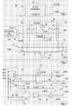
- a circuit integrated 10 contains a volatile memory 12 which is represented, for purposes of illustration, by a plan memory 14 and an interface logic circuit 16.
- the memory array 14 is for example constituted of an array of memory elements volatile.
- the interface logic circuit 16 comprises the set components adapted to address memory elements volatile to write or read data in elements of volatile memory.
- the memory 12 is connected with two separate power supplies.
- a power supply corresponds to a supply voltage or torque formed by a supply voltage and a voltage of reference, commonly GND mass.
- a first voltage Vdd_M supply is provided to the memory plane 14 and a second supply voltage Vdd_I is supplied to the circuit interface logic 16.
- the supply voltages Vdd_M and Vdd_I can be ordered independently and, in in particular, be set at different values.
- FIG. 2 shows in more detail a volatile memory element 20 of the memory plane 14 of FIG. 1 and components 22 of the interface logic circuit 16 used for writing and / or reading data in the element of FIG. volatile memory 20.
- the volatile memory element 20 shown is an element of a static random-access memory (SRAM) and includes inver- ally connected inverters 24, 26.
- the respective inputs of the inverters 24, 26 are connected to respective bit lines BL, BL , Via switches 28 controlled by a row select signal conveyed by a word line WL.
- Each inverter 24, 26 is powered by a high voltage Vdd_M and the reference voltage GND.
- a volatile memory element 20 may consist of six MOS transistors, each inverter 24, 26 comprising two complementary MOS transistors.
- the components 22 of the interface logic circuit 16 include a line decoder 32 connected to an inverter 34 which provides the row selection signal carried by the word line WL.
- Bit lines BL and BL constitute the inputs 36, 38 of a sense amplifier 40.
- the inputs 36, 38 of the amplifier 40 are connected to the voltage Vdd_I by means of precharge transistors 42 controlled by a precharge signal carried by a line of preload PL.
- one of the bit lines BL or BL the voltage Vdd_M and on the other the voltage GND.
- the switches 28 are then closed to set the state of the inputs and outputs of the inverters 24, 26.
- the switches 28 are then opened and the state of the signals across the inverters 24, 26 is maintained.
- each bit line BL and BL is, for example, preloaded at a voltage between the voltages Vdd_M and GND, then the switches 28 are closed so that the voltages on the bit lines vary according to the state of the signals across the inverters 24, 26.
- the sense amplifier 40 provides binary information related to the information stored in the volatile memory element 20.
- the present invention provides a command independent of the supply voltages Vdd_M and Vdd_I.
- the voltages supply Vdd_M and Vdd_I each have a nominal level.
- the power supply of the logic circuit interface 16 may be interrupted, which corresponds to a resetting the voltage Vdd_I.
- the power of the memory plane 14 is not interrupted so as not to lose the information stored in the memory plane 14.
- the voltage Vdd_M power supply can be decreased relative to the level active up to a minimum level of no loss of information.
- the present invention makes it possible to use MOS transistors of different types for memory elements volatile 20 of the memory plane 14 and for the logic circuit 16.
- MOS transistors of different types for memory elements volatile 20 of the memory plane 14 and for the logic circuit 16.
- different types of transistors are usually offered to designers of integrated circuits according to whether they favor a speed of high transistor switching or weak currents of leak.
- transistors called interface transistors or high-voltage transistors which have a greater gate oxide thickness than the gate oxide thickness of other fabricated transistors according to the same technology, and subsequently called transistors to thin grid.
- High-voltage transistors are usually controlled by gate voltages higher than the voltages used with thin gate MOS transistors.
- the leakage currents that appear with a high voltage transistor are less important than for a thin gate transistor.
- switching speed of a high voltage transistor is generally lower than that of a gate transistor slim.
- thin-gate transistors are used for the realization of logic circuits and memories of a integrated circuit. High voltage transistors are usually used to interface between digital and analog parts of an integrated circuit.
- the fourth type corresponds to the transistor high voltage which has a higher gate thickness.
- high-voltage transistors for producing the elements of volatile memory 20 of the memory array 14. decrease of the leakage currents in the memory plane 14.
- the voltage Vdd_M is nevertheless chosen greater than the voltage Vdd_I in active mode.
- the interface logic circuit 16 therefore consists of fast transistors powered by a supply voltage Vdd_I which is switched off in idle mode.
- Vdd_M inactive mode it is advantageous to reduce the supply voltage Vdd_M inactive mode to minimize the static consumption of memory 12.
- Vdd_M substantially equal to 3.3 volts in active mode and 0.9 volts in inactive mode
- Vdd_I substantially equal to 1.8 volts in active mode and substantially zero in mode inactive.
- Vdd_M it may be preferable to maintain the supply voltage Vdd_M at a high level even in idle mode. Indeed, especially for cell phone applications, it is generally expected that a single battery that provides active mode directly the supply voltage Vdd_M and which is connected to a regulator voltage step down to supply the supply voltage Vdd_I. In idle mode, to provide a supply voltage Vdd_M decreased, it would be necessary to use a regulator voltage booster, the operation of which would lead to a overconsumption more important than consumption gains obtained by decreasing the supply voltage Vdd_M.
- FIG. 3 represents another exemplary embodiment of the invention in which the integrated circuit 10 comprises a volatile memory element 50, interface circuits 52 connected to the volatile memory element 50, and a circuit logic 54 performing logical operations without relation direct with the operation of the volatile memory element
- the volatile memory element 50 is consisting of a flip-flop 56 controlled by a clock signal CLK.
- the interface circuits 52 comprise a multiplexer 58 with four inputs DIO, DI1, DI2 and DI3, receiving a selection signal MI, and providing one of the input signals DIO to DI3 at flip-flop 56.
- Interface circuits 52 two inverters 60, 62 receiving two complementary output provided by flip-flop 56. Inverters 60, 62 provide output data DO1 and DO2.
- the circuit logic 54 comprises a NAND logic gate 64 receiving the DI0 and DI4 signals and a NOR logic gate 66 receiving the DI3 signal and DI5 input signal.
- a NAND logic gate 68 receives the outputs of logic gates 64, 66.
- the output of the logic gate 68 is provided to an inverter 70 which provides a output signal DO3.
- Vdd_M three separate power supplies, Vdd_M, Vdd_I and Vdd_L, respectively for the volatile memory element 50, the interface circuits 52 and the logic circuit 54.
- the present example of the invention can use three different types of transistors. of the high voltage transistors resulting in low currents of leakage are used for the volatile memory element 50. Thin gate transistors are used for circuits interface 52 and the logic circuit 54. For example, according to the aim, the use of transistors thin gate having a high switching speed for the logic circuit 54 and thin-gate and low-gate transistors leakage current for the interface circuits 52.
- the three distinct power supplies Vdd_M, Vdd_I and Vdd_L are therefore each associated with a family of particular transistors.
- the integrated circuit may include non-memory elements volatile and a power supply connected to non memory elements volatile distinct from the memory element power volatile. This is for example the same connected power supply to the logic circuits interfaced with the volatile memory. The power supply connected to the non-volatile memory elements is then off in idle mode.
- volatile memory elements are memory elements volatile logical. It is clear that the elements of memory volatile can be volatile memory elements analog and associated circuits indifferently type logic or analog.
- the interface circuits connected to the volatile memory elements are logical interface circuits. It is clear that interface circuits can be interface circuits analog or analog mixed interface circuits and digital.
- the present invention is capable of various variations and modifications that will appear to man art.
- the power supplies may consist of adjustable current sources.
- the reference voltage is the same for the volatile memory, the interface logic circuit and the logic circuit 54. This is not a necessary condition and the volatile memory, the interface logic circuit and the logic circuit 54 can be connected to voltages of different reference.
Landscapes
- Engineering & Computer Science (AREA)
- Power Engineering (AREA)
- Static Random-Access Memory (AREA)
- Semiconductor Memories (AREA)
- Logic Circuits (AREA)
Abstract
Description
Claims (10)
- Circuit intégré (10) comportant des éléments de mémoire volatile (20, 50) et des circuits d'interface (16, 22, 52) reliés aux éléments de mémoire volatile, comprenant des première et deuxième alimentations distinctes (Vdd_M, Vdd_I), la première alimentation étant connectée aux éléments de mémoire volatile et la deuxième alimentation étant connectée aux circuits d'interface et dans lequel les éléments de mémoire volatile (20, 50) comprennent des transistors MOS (28) d'un premier type, et les circuits d'interface (22, 52, 54) comprennent des transistors MOS (42) d'un deuxième type différent du premier type.
- Circuit intégré selon la revendication 1, comprenant des moyens pour éteindre la deuxième alimentation (Vdd_I) et pour mettre la première alimentation (Vdd_M) à un niveau minimal non nul adapté à assurer la conservation des informations stockées dans les éléments de mémoire volatile (20, 50), dans un mode de fonctionnement déterminé.
- Circuit intégré selon la revendication 1, dans lequel les transistors du premier type ont une épaisseur d'oxyde de grille supérieure à l'épaisseur d'oxyde de grille des transistors du deuxième type ou les transistors du premier type ont chacun une zone active de canal dopée pour fournir des courants de fuite plus faibles que pour les transistors du deuxième type.
- Circuit intégré selon la revendication 3, comprenant des moyens pour mettre les première et deuxième alimentations (Vdd_M, Vdd_I) à des niveaux non nuls dans un mode de fonctionnement déterminé, la première alimentation (Vdd_M) étant à un niveau différent du niveau de la deuxième alimentation (Vdd_I) .
- Circuit intégré selon la revendication 1, comprenant des circuits logiques supplémentaires (54), et une troisième alimentation (Vdd_L), distincte des première et deuxième alimentations (Vdd_M, Vdd_I), connectée aux circuits logiques supplémentaires.
- Circuit intégré selon la revendication 5, comprenant des moyens pour éteindre la troisième alimentation (Vdd_L) et maintenir les première et deuxième alimentations (Vdd_M, Vdd_I) à un niveau non nul dans un mode de fonctionnement déterminé.
- Circuit intégré selon la revendication 5, comprenant des moyens pour éteindre les deuxième et troisième alimentations (Vdd_I, Vdd_L) et mettre la première alimentation (Vdd_M) à un niveau minimal non nul adapté à assurer la conservation des informations stockées dans les éléments de mémoire volatile (20, 50) dans un mode de fonctionnement déterminé.
- Circuit intégré selon les revendications 3 et 5, dans lequel les circuits logiques supplémentaires (54) comprennent des transistors d'un troisième type, les transistors du premier type ayant une épaisseur d'oxyde de grille supérieure à l'épaisseur d'oxyde de grille des transistors du troisième type ou les transistors du premier type ayant chacun une zone active de canal dopée pour fournir des courants de fuite plus faibles que pour les transistors du troisième type, les transistors du troisième type ayant une vitesse de commutation supérieure à la vitesse de commutation des transistors du deuxième type.
- Circuit intégré selon la revendication 8, comprenant des moyens pour mettre les première, deuxième et troisième alimentations (Vdd_M, Vdd_I, Vdd_L) à des niveaux différents.
- Procédé de commande en mode de veille d'un circuit intégré (10) comprenant des éléments de mémoire volatile (20, 50) et des circuits d'interface (16, 22, 52) reliés aux éléments de mémoire volatile, caractérisé en ce qu'il comprend les étapes suivantes :prévoir une première alimentation (Vdd_M) connectée aux éléments de mémoire volatile ;prévoir une deuxième alimentation (Vdd_I), distincte de la première alimentation, connectée aux circuits d'interface ;prévoir, pour les éléments de mémoire volatile (20, 50), des transistors MOS (28) d'un premier type, et, pour les circuits d'interface (22, 52, 54), des transistors MOS (42) d'un deuxième type différent du premier type ; etéteindre la deuxième alimentation et mettre la première alimentation à un niveau minimal non nul adapté à assurer la conservation des informations stockées dans les éléments de mémoire volatile (20, 50).
Applications Claiming Priority (2)
| Application Number | Priority Date | Filing Date | Title |
|---|---|---|---|
| FR0351194A FR2864684B1 (fr) | 2003-12-24 | 2003-12-24 | Circuit integre a memoire a consommation reduite |
| FR0351194 | 2003-12-24 |
Publications (1)
| Publication Number | Publication Date |
|---|---|
| EP1560220A1 true EP1560220A1 (fr) | 2005-08-03 |
Family
ID=34639750
Family Applications (1)
| Application Number | Title | Priority Date | Filing Date |
|---|---|---|---|
| EP04106884A Withdrawn EP1560220A1 (fr) | 2003-12-24 | 2004-12-22 | Circuit intégré à mémoire à consommation réduite |
Country Status (3)
| Country | Link |
|---|---|
| EP (1) | EP1560220A1 (fr) |
| JP (1) | JP2005190651A (fr) |
| FR (1) | FR2864684B1 (fr) |
Families Citing this family (1)
| Publication number | Priority date | Publication date | Assignee | Title |
|---|---|---|---|---|
| KR102275497B1 (ko) | 2014-10-20 | 2021-07-09 | 삼성전자주식회사 | 전원 경로 제어기를 포함하는 시스템 온 칩 및 전자 기기 |
Citations (3)
| Publication number | Priority date | Publication date | Assignee | Title |
|---|---|---|---|---|
| US5726562A (en) * | 1995-09-07 | 1998-03-10 | Nec Corporation | Semiconductor device and power supply controller for same |
| US5740118A (en) * | 1995-11-22 | 1998-04-14 | Fujitsu Limited | Semiconductor memory device |
| US20030218915A1 (en) * | 2002-05-23 | 2003-11-27 | Matsushita Electric Industrial Co., Ltd. | Semiconductor device adapted for power shutdown and power resumption |
-
2003
- 2003-12-24 FR FR0351194A patent/FR2864684B1/fr not_active Expired - Fee Related
-
2004
- 2004-12-22 EP EP04106884A patent/EP1560220A1/fr not_active Withdrawn
- 2004-12-24 JP JP2004374920A patent/JP2005190651A/ja active Pending
Patent Citations (3)
| Publication number | Priority date | Publication date | Assignee | Title |
|---|---|---|---|---|
| US5726562A (en) * | 1995-09-07 | 1998-03-10 | Nec Corporation | Semiconductor device and power supply controller for same |
| US5740118A (en) * | 1995-11-22 | 1998-04-14 | Fujitsu Limited | Semiconductor memory device |
| US20030218915A1 (en) * | 2002-05-23 | 2003-11-27 | Matsushita Electric Industrial Co., Ltd. | Semiconductor device adapted for power shutdown and power resumption |
Also Published As
| Publication number | Publication date |
|---|---|
| FR2864684B1 (fr) | 2006-06-23 |
| JP2005190651A (ja) | 2005-07-14 |
| FR2864684A1 (fr) | 2005-07-01 |
Similar Documents
| Publication | Publication Date | Title |
|---|---|---|
| EP0080394B1 (fr) | Bascule bistable à stockage non volatil et à repositionnement statique | |
| EP1833090B1 (fr) | Cellules mémoire en technologie CMOS double-grille dotée de transistors à deux grilles independantes | |
| US8995215B2 (en) | Semiconductor device and control method of the same | |
| FR2712421A1 (fr) | Circuit de commande d'une ligne de mots pour dispositif de mémoire à semi-conducteur. | |
| EP3217407B1 (fr) | Cellule memoire sram comprenant un n-tfet et un p-tfet | |
| EP3010022B1 (fr) | Cellule memoire a transistors de lecture de type tfet et mosfet | |
| FR2849260A1 (fr) | Cellule de memoire sram non volatile. | |
| FR2517143A1 (fr) | Bascule bistable a stockage non volatil et a repositionnement dynamique | |
| FR2986652A1 (fr) | Memoire volatile a consommation reduite et capacite de stockage amelioree | |
| US20070133256A1 (en) | Integrated circuit with a memory of reduced consumption | |
| EP1560220A1 (fr) | Circuit intégré à mémoire à consommation réduite | |
| EP1465200B1 (fr) | Cellule mémoire statique à accès aléatoire (SRAM), et unité mémoire à ultra basse consommation réalisée à partir de telles cellules | |
| FR2894708A1 (fr) | Memoire a cellule memoire a transistor mos a corps isole | |
| FR2751778A1 (fr) | Memoire accessible en lecture seulement | |
| FR2750240A1 (fr) | Generateur de reference de tension | |
| EP2003650A1 (fr) | Cellule mémoire SRAM asymétrique à 4 transistors double grille | |
| FR2897193A1 (fr) | Circuit de fusible electrique procurant une fonction de lecture de marge | |
| EP1650806B1 (fr) | Cellule de mémoire volatile préenregistrée. | |
| EP1168359B1 (fr) | Procédé de commande d'un accès en lecture d'une mémoire vive dynamique et mémoire correspondante. | |
| FR3130449A1 (fr) | Dispositif de pilotage de transistors et procédé de pilotage | |
| EP1624460B1 (fr) | Mémoire comprenant un point mémoire de type SRAM, procédé de lecture et procédé d'écriture associés. | |
| EP1398793B1 (fr) | Circuit intégré numérique réalisé en technologie MOS | |
| FR3145423A1 (fr) | Procédé de gestion de mémoire pour économiser de l'énergie | |
| FR3146541A1 (fr) | Procédé de lecture d'une mémoire | |
| FR3146542A1 (fr) | Dispositif mémoire |
Legal Events
| Date | Code | Title | Description |
|---|---|---|---|
| PUAI | Public reference made under article 153(3) epc to a published international application that has entered the european phase |
Free format text: ORIGINAL CODE: 0009012 |
|
| AK | Designated contracting states |
Kind code of ref document: A1 Designated state(s): AT BE BG CH CY CZ DE DK EE ES FI FR GB GR HU IE IS IT LI LT LU MC NL PL PT RO SE SI SK TR |
|
| AX | Request for extension of the european patent |
Extension state: AL BA HR LV MK YU |
|
| RIN1 | Information on inventor provided before grant (corrected) |
Inventor name: POLLET, JEAN-FRANCOIS Inventor name: BONZO, ANDREA |
|
| AKX | Designation fees paid | ||
| 17P | Request for examination filed |
Effective date: 20060203 |
|
| RBV | Designated contracting states (corrected) |
Designated state(s): DE FR |
|
| REG | Reference to a national code |
Ref country code: DE Ref legal event code: 8566 |
|
| 17Q | First examination report despatched |
Effective date: 20100310 |
|
| STAA | Information on the status of an ep patent application or granted ep patent |
Free format text: STATUS: THE APPLICATION IS DEEMED TO BE WITHDRAWN |
|
| 18D | Application deemed to be withdrawn |
Effective date: 20100103 |