EP1560327B1 - Dispositif de prédistortion à bandes multiples avec tables de correspondance - Google Patents
Dispositif de prédistortion à bandes multiples avec tables de correspondance Download PDFInfo
- Publication number
- EP1560327B1 EP1560327B1 EP05001623A EP05001623A EP1560327B1 EP 1560327 B1 EP1560327 B1 EP 1560327B1 EP 05001623 A EP05001623 A EP 05001623A EP 05001623 A EP05001623 A EP 05001623A EP 1560327 B1 EP1560327 B1 EP 1560327B1
- Authority
- EP
- European Patent Office
- Prior art keywords
- band
- signals
- look
- predistorter
- signal
- Prior art date
- Legal status (The legal status is an assumption and is not a legal conclusion. Google has not performed a legal analysis and makes no representation as to the accuracy of the status listed.)
- Expired - Lifetime
Links
Images





Classifications
-
- H—ELECTRICITY
- H03—ELECTRONIC CIRCUITRY
- H03F—AMPLIFIERS
- H03F1/00—Details of amplifiers with only discharge tubes, only semiconductor devices or only unspecified devices as amplifying elements
- H03F1/32—Modifications of amplifiers to reduce non-linear distortion
- H03F1/3241—Modifications of amplifiers to reduce non-linear distortion using predistortion circuits
- H03F1/3252—Modifications of amplifiers to reduce non-linear distortion using predistortion circuits using multiple parallel paths between input and output
-
- H—ELECTRICITY
- H04—ELECTRIC COMMUNICATION TECHNIQUE
- H04B—TRANSMISSION
- H04B1/00—Details of transmission systems, not covered by a single one of groups H04B3/00 - H04B13/00; Details of transmission systems not characterised by the medium used for transmission
- H04B1/62—Details of transmission systems, not covered by a single one of groups H04B3/00 - H04B13/00; Details of transmission systems not characterised by the medium used for transmission for providing a predistortion of the signal in the transmitter and corresponding correction in the receiver, e.g. for improving the signal/noise ratio
-
- H—ELECTRICITY
- H03—ELECTRONIC CIRCUITRY
- H03F—AMPLIFIERS
- H03F1/00—Details of amplifiers with only discharge tubes, only semiconductor devices or only unspecified devices as amplifying elements
- H03F1/32—Modifications of amplifiers to reduce non-linear distortion
-
- H—ELECTRICITY
- H03—ELECTRONIC CIRCUITRY
- H03F—AMPLIFIERS
- H03F1/00—Details of amplifiers with only discharge tubes, only semiconductor devices or only unspecified devices as amplifying elements
- H03F1/32—Modifications of amplifiers to reduce non-linear distortion
- H03F1/3241—Modifications of amplifiers to reduce non-linear distortion using predistortion circuits
-
- H—ELECTRICITY
- H03—ELECTRONIC CIRCUITRY
- H03F—AMPLIFIERS
- H03F1/00—Details of amplifiers with only discharge tubes, only semiconductor devices or only unspecified devices as amplifying elements
- H03F1/32—Modifications of amplifiers to reduce non-linear distortion
- H03F1/3241—Modifications of amplifiers to reduce non-linear distortion using predistortion circuits
- H03F1/3247—Modifications of amplifiers to reduce non-linear distortion using predistortion circuits using feedback acting on predistortion circuits
-
- H—ELECTRICITY
- H03—ELECTRONIC CIRCUITRY
- H03F—AMPLIFIERS
- H03F3/00—Amplifiers with only discharge tubes or only semiconductor devices as amplifying elements
- H03F3/189—High-frequency amplifiers, e.g. radio frequency amplifiers
-
- H—ELECTRICITY
- H03—ELECTRONIC CIRCUITRY
- H03F—AMPLIFIERS
- H03F2201/00—Indexing scheme relating to details of amplifiers with only discharge tubes, only semiconductor devices or only unspecified devices as amplifying elements covered by H03F1/00
- H03F2201/32—Indexing scheme relating to modifications of amplifiers to reduce non-linear distortion
- H03F2201/3233—Adaptive predistortion using lookup table, e.g. memory, RAM, ROM, LUT, to generate the predistortion
Definitions
- the present invention relates to a multi-band predistorter that permits amplification of all transmission signals of multiple frequency bands by a common amplifier.
- One of known compensation method for nonlinear distortions by microwave power amplifiers is a predistortion method using a digital signal processing scheme (hereinafter referred to as a digital predistortion method) (for example, Japanese patent application laid open No. 2002-522989, hereinafter referred to as patent document 1).
- the digital predistortion method features elimination of the need for complex analog circuitry by implementing a predistorter configuration through utilization of digital signal processing.
- Linear amplifier realizations have been achieved mostly by use of analog circuits such as a feed-forward amplifier, a negative feed-back amplifier, and so forth.
- Predistorters have also been formed by analog circuits (for example, H. Girard and K.
- non-patent document 1 No. 1, 1983, hereinafter referred to as non-patent document 1
- Nojima and Okamoto "Analysis and Compensation of TWT Nonlinearities Based on Complex Power Series Representation”
- linearizer technologies using such analog circuits generally require a high accuracy by adjusting technique.
- the analog circuits need to be simplified for miniaturization and economization of a transmitter containing a modulation circuit.
- the look-up table type predistorter achieves distortion compensation over a frequency range of only 20 MHz or so about the carrier frequency.
- the PDC Personal Digital Cellular
- the look-up table type predistorter needs to be built for each frequency band, and a vector signal modulator, a frequency converter, and a power amplifier are also required for each band ⁇ this inevitably causes the defects of bloated device scale, higher power consumption and increased device bulkiness.
- a multi-band look-up table type predistorter which comprises:
- the present invention it is possible to achieve correct distortion compensation for each frequency band by separating the input signal containing multiple frequency band signals by means of band signal extractors into signals of the respective frequency bands and making compensation in each band on the basis of distortion compensation value that is read out of the look-up table provided for each band.
- the signals of the respective frequency bands are combined by the combiner after being added with the corresponding compensation values, the combined output can be amplified by a common amplifier. This permits simplification of the equipment configuration, reduction of power consumption and equipment miniaturization.
- Fig. 1 illustrates in block form the basic configuration of the look-up table type predistorter that carries out the present invention in the best mode.
- the predistorter according to the present invention can be configured to handle signals of two or more discrete frequency bands, simultaneously. In the interests of brevity of description, the predistorter will hereinafter be assumed to be compatible with signals of two frequency bands.
- the look-up table type predistorter is comprised of: band signal extractors 11-1 and 11-2 for extracting band signals from an input signal S T of two transmission frequency bands; difference detectors 16-1 and 16-2 for detecting differences between the band signals extracted by the band signal extractors 11-1 and 11-2 and signals of the corresponding frequency bands extracted from the output signal from the power amplifier (not shown) whose distortion is to be cancelled by the predistorter; frequency band look-up tables 17-1 and 17-2 from which compensation data D 1 and D 2 are read out for compensating for distortions (i.e., performing predistortion) of the transmission signals of the corresponding frequency bands by using detected signals from the difference detectors 16-1 and 16-2 as reference signals; adders 13-1 and 13-2 for adding the compensation data D 1 , D 2 read out of the look-up tables 17-1 and 17-2 to the transmission signals of the respective transmit frequency bands; and a combiner 14 for combining the added outputs into the output from the predistorter.
- the input transmission signal S T is applied via a divider 10 to the two band signal extractors 11-1 and 11-2 to extract signals of two frequency bands.
- the one of the two extracted signals is divided by a divider 12-1 into two, one of which is applied to the adder 13-1 and the other of which is applied to the difference detector 16-1.
- the other extracted signal is divided by a divider 12-2 into two, one of which is applied to the adder 13-2 and the other of which is applied to the difference detector 16-2.
- the divided transmission signals of the respective frequency bands provided to the adders 13-1 and 13-2 are combined by the combiner 14 into a predistorter output signal S D , which is supplied to a power amplifier (not shown).
- the band signal extractors 15-1 and 15-2 extract signals of the same frequency bands as those of the signals extracted by the band signal extractors 11-1 and 11-2.
- the output signals from the band signal extractors 15-1 and 15-2 are applied to the difference detectors 16-1 and 16-2, respectively.
- the difference detectors 16-1 and 16-2 detect differences e 1 and e 2 between the transmission signals and the amplifier output signals in the frequency bands corresponding thereto. Accordingly, the distortion components generated by the power amplifier in the respective frequency bands are detected as the difference signals.
- the thus detected differences e 1 and e 2 in the respective frequency bands are used as reference signals to read out corresponding compensation data D 1 and D 2 from the look-up tables 17-1 and 17-2, and the read-out pieces of compensation data are provided to the adders 13-1 and 13-2.
- These compensation data are those which cancel the detected distortion components; in the look-up tables 17-1 and 17-2 there are prestored predetermined compensation data for distortion components that the power amplifier generates in the respective frequencies.
- the suppression of distortion is adaptively reduced by repeatedly updating these compensation data for each frequency band until a predetermined amount of distortion is suppressed.
- the difference signals e 1 and e 2 detected by the difference detectors 16-1 and 16-2 are provided as reference signals to the look-up tables 17-1 and 17-2 to read out therefrom distortion compensation data D 1 and D 2 in the respective frequency bands, which are added by the adders 13-1 and 13-2 to the signals of the frequency bands to be transmitted to implement distortion compensation (i.e., predistortion).
- the transmission signals added by the adders 13-1 and 13-2 with the distortion compensation data are combined by the combiner 14, and the combined output is converted to an analog signal, which is amplified by a predetermined power amplifier and then transmitted.
- signals of 800-MHz and 1.5-GHz bands can be used as the band signals that are extracted by the band signal extractors 11-1 and 11-2.
- the number of frequency bands is not limited specifically to two.
- the number of band signal extractors is four, and consequently the numbers of dividers 12, adders 13, difference detectors 16 and look-up tables 17 are also four, respectively.
- the band signal extractors 11-1, 12-1 and 15-1 15-2 have desired bandwidths of center frequencies at f1 and f2, and extract signals of first and second frequency bands, respectively.
- Such band signal extractors may each be formed, for instance, by a band pass filter (BPF), or band elimination filter (BEF).
- BPF band pass filter
- BEF band elimination filter
- frequency-attenuation characteristics of the first and second frequency band signal extractors 11-1 and 12-1 (or 15-1 and 15-2), each formed by the BPF are conceptually shown by solid and broken lines, respectively. It can be seen that the amount of attenuation sharply increases outside the frequency bands of the center frequencies f1 and f2, providing sufficient spacing between the frequency bands. Such characteristics of a BPF can usually be obtained by a cascade connection of multiple BPFs.
- Fig. 3 shows frequency-attenuation characteristics of the first frequency band signal extractor 11-1 formed by a BEF, for instance.
- This example conceptually shows the characteristic that the first frequency band signal extractor 11-1 is required to have in the case of using four frequency bands of center frequencies f1, f2, f3 and f4.
- the illustrated characteristic can be obtained, as is evident from Fig. 3, by such a cascade connection of three BEFs BEF1, BEF2 and BEF3 as shown in Fig. 4 which eliminate the second, third and fourth frequency bands, except the first frequency band.
- Each band elimination filter is so configured as to have a sufficient band elimination characteristic in the corresponding band and a sufficiently low-loss pass characteristic in the other bands.
- Such a band elimination filter can be formed, for example, by a notch filter.
- the notch filter is a BEF using a dielectric resonator, a filter using a stub formed by a microstrip line, or the like.
- the characteristic of the second frequency band signal extractor 12-1 can also be obtained similarly by a cascade connection of three BEFs that eliminate the first, third and fourth frequency bands. The same holds true for third and fourth frequency band signal extractors that are not shown.
- each frequency band signal extractor facilitates extraction of a signal around the center frequency and makes it relatively easy to provide isolation between the center frequencies of adjacent frequency bands.
- the center frequency is the resonance frequency of the BPF
- a signal delay increases, giving rise to the problem of difficulty in designing feedback paths containing the band signal extractors 15-1 and 15-2.
- the signal delay is small because the BEF has no center frequency in the frequency band. This allows ease in designing BEF as well as the feedback paths.
- the band signal extractors may be formed by BPFs, or BEFs.
- Fig. 5 illustrates in block form a second embodiment of the present invention, in which the look-up table type predistorter, surrounded by the broken line is formed by digital circuits. Because of the digital signal processing system, I and Q signal paths are provided. At the input side two digital transmitters T-1 and T-2 are provided, from which a first frequency band signal S T1 of the center frequency f1 and a second frequency band signal S T2 of the center frequency f2 are input to the predistorter. In the application of the predistorter to mobile communications, the first and second frequency band signals of the center frequencies f1 and f2 may be 800-MHz and 1.5-GHz band signals, respectively. The input signals are not limited specifically to these two waves, but other frequency band signals such as 2-GHz, 5-GHz and so on can also be used.
- the band signals output from the transmitters T-1 and T-2 are combined by a combiner 9, and the combined signal S T is input to the look-up table type digital predistorter. Since the internal configuration of the predistorter is identical with that shown in Fig. 1, the corresponding parts are denoted by the same reference numerals and their description will not be repeated.
- the band signal extractors 11-1, 11-2 and 15-1, 15-2 each formed by a BEF of digital signal processing, it is possible to achieve sufficient band elimination at the center frequency of each filter.
- the combined signals by the combiner 14 is converted by digital-to-analog converter (DAC) 24-1 and 24-2 to analog signals.
- DAC digital-to-analog converter
- the converted analog signals are subjected to vector modulation by a vector signal modulator 25, and the vector-modulated signal is applied to a frequency converter 26, wherein it is subjected to frequency conversion by a carrier signal from a local oscillator 27.
- the thus frequency-converted high-frequency signal is amplified by a power amplifier 28, from which it is sent via a duplexer (not shown) to an antenna (not shown).
- a directional coupler 29 by which a portion of the transmission signal is branched as a monitor signal S M .
- the monitor signal S M is demodulated by a monitoring receiver 31, and the demodulated monitor signal is converted by analog-to-digital converters (ADC) 32-1 and 32-2 to I and Q signals (i.e., an in-phase signal and a quadrature signal) in digital form.
- ADC analog-to-digital converters
- I and Q signals i.e., an in-phase signal and a quadrature signal
- the I and Q signals are input to the multi-band look-up table type digital predistorter.
- signals corresponding to the distortion components in the transmission signal by the power amplifier 28 are added beforehand to the transmission signal in a 180° out-of-phase relation thereto in the multi-band look-up table type predistorter. This enables the distortion components to be cancelled in the amplification of the transmission signal by the power amplifier 28.
- the band signal extractors 11-1 and 11-2 need not always be provided, but instead the transmission signals of the respective frequency bands are applied directly from the transmitters T-1 and T-2 to the dividers 12-1 and 12-2 as indicated by the broken lines.
- the output signals from the digital predistorter may be subjected to digital-to-analog conversion independently of each other, then subjected to frequency conversion by independent frequency converters, and combined by a wide-band directional coupler or power combiner.
- the coefficients prestored as compensation data in the look-up tables 17-1 and 17-2 are obtained by pre-measuring the input/output characteristics of the power amplifier 28 for each frequency band.
- the coefficients in the look-up tables 17-1 and 17-2 are corrected until a predetermined amount of suppression of distortion is reached for each frequency band. By repeating such a process the suppression of distortion is adaptively decreased for each frequency band.
- the intermodulation distortions which are created by the input signals of multiple bands in the power amplifier 28, can be cancelled by a duplexer or band pass filter at the output side of the power amplifier 28 since adjacent frequency bands are sufficiently spaced apart.
- Fig. 6 illustrates in block form another embodiment of the present invention, which is a multi-band look-up table type analog predistorter formed by analog circuits. Since the look-up tables 17-1 and 17-2 are implemented by digital signal processing, the reference signals are obtained by frequency converting high-frequency difference signals e 1 and e 2 by down converters 33-1 and 33-2 to base band signals and converting the base band signals by analog-to-digital converters (ADC) 43-1 and 34-2 to digital signals.
- ADC analog-to-digital converters
- the compensation data D1 and D 2 read out of the look-up tables 17-1 and 17-2 are converted by digital-to-analog converters (DAC) 35-1 and 35-2 to analog signals, which are converted by up converters 36-1 and 36-2 to high-frequency signals D 1 and D 2 , which are applied to the adders 13-1 and 13-2.
- DAC digital-to-analog converters
- the part surrounded by the broken line is basically identical with the Fig. 1 configuration except the above.
- the output from the predistorter is amplified by the power amplifier 28, and the amplifier output is provided to a duplexer (not shown) connected to an antenna (not shown).
- the directional coupler 29 at the output side of the power amplifier 28 branches a portion of the transmission signal, which is input to the analog predistorter.
- the band signal extractors 11-1 and 11-2 need not always be provided.
- the output signals from the analog predistorter may be frequency converted by independent frequency converters, and combined by a wide-band directional coupler or power combiner.
- the coefficients in the look-up tables 17-1 and 17-2 are obtained by pre-measuring the input/output characteristics of the power amplifier 28 for each frequency band.
- the coefficients in the look-up tables 17-1 and 17-2 are corrected until a predetermined amount of suppression of distortion is reached for each frequency band. By repeating such a process the suppression of distortion is adaptively decreased for each frequency band.
- intermodulation distortions which are created by the input signals of multiple frequency bands in the power amplifier 28, can be cancelled by a duplexer or BPF at the output side of the power amplifier 28 since adjacent frequency bands are sufficiently spaced apart.
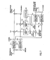
- Fig. 7 illustrates in block form another embodiment of the present invention, which is adapted to update the look-up tables 17-1 and 17-2 in the Fig. 1 embodiment.
- the output signals from the difference detectors 16-1 and 16-2 are applied to dividers 23-1 and 23-2, from which divided difference detected signals e 1 and e 2 are provided to a controller 22, which updates the look-up tables 17-1 and 17-2 on the basis of the difference detected signals e 1 and e 2 .
- the difference detected signals e 1 and e 2 which is used as reference signals for the look-up tables 17-1 and 17-2, are input to the controller 22.
- the controller 22 controls updating of the coefficients of the compensation data in the look-up tables 17-1 and 17-2 in such a manner as to minimize the reference signals that are input to the controller 22.
- Eq. (3) is a control algorithm stored in the controller 22.
- the controller 22 updates coefficients in the look-up table in such a manner as to minimize the absolute value of the reference signal matrix E(t). That is, instead of updating the coefficients in the look-up tables for the individual frequencies to minimize the reference signal e i (t), the coefficients in all of the look-up tables are updated to minimize the reference signal matrix E(t).
- the forgetting coefficient matrix ⁇ (t) is calculated such that the absolute value of the reference signals matrix becomes minimized. This enables simultaneous compensation for distortions in the N frequency bands.
- Eq. (3) is not intended for updating the coefficients in the individual look-up tables.
- a second updating method which is a control method for minimizing the reference signals that are input to the respective look-up tables.
- the controller 22 sets the forgetting coefficients at fixed values as given by the following equation (5).
- W ( t ) W ( t ) + ⁇ E ( t )
- the coefficients in the look-up tables for the respective frequency bands are independently controlled in a manner to minimize the corresponding reference signals.
- updating of the coefficients of the multiple look-up tables by Eq. (5) may be carried out simultaneously or in a sequential order. In the latter case, the coefficients are controlled one at a time.
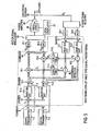
- Fig. 8 illustrates in block form still another embodiment of the present invention, which is adapted to update the look-up tables 17-1 and 17-2 in the Fig. 5 embodiment.
- the dividers 23-1 and 23-2 and the controller 22 are provided.
- a portion of the output from the power amplifier 28 is extracted by the directional coupler 26 as the monitor signal S M , which is frequency-converted by the monitoring receiver 31 to base band signals.
- the base band signals are converted by the analog-to-digital converters (ADC) 32-1 and 32-2 to digital signals.
- ADC analog-to-digital converters
- the differences between the digital signals and the signals divided by the dividers 12-1 and 12-2 are detected as the reference signals e 1 and e 2 by the difference detectors 16-1 and 16-2.
- the reference signals e 1 and e 2 and the control signals from the controller 22 are used to update the coefficients of the look-up tables 17-1 and 17-2 and to read out therefrom the compensation data. This sequence of signal processing steps is performed for each transmission frequency band. In this way, independent distortion compensation can be implemented for the transmission signal of each frequency band.
- the combiner 9 and the divider 10 are unnecessary, and the transmission signals are supplied directly to the dividers 12-1 and 12-2 as indicated by the broken lines.
- the output signals from the digital predistorter may be subjected to digital-to-analog conversion independently of each other, then subjected to frequency conversion by independent frequency converters, and combined by a wide-band directional coupler or power combiner.
- the controller 22 instructs the two look-up tables 17-1 and 17-2 to update their coefficients in a manner to minimize the sum of absolute values of the reference signals e 1 and e 2 in the two frequency bands.
- the instructions for updating the coefficients of the look-up tables 17-1 and 17-2 may be coefficients that minimize the absolute values of the reference signals e 1 and e 2 .
- the initial coefficients of the look-up tables 17-1 and 17-2 are obtained by pre-measuring the input/output characteristics of the power amplifier 28 for each frequency band.
- the coefficients of the look-up tables 17-1 and 17-2 are corrected until a predetermined amount of suppression of distortion is reached for each frequency band. By repeating such a process the suppression of distortion is adaptively decreased for each frequency band.
- the intermodulation distortions which are created by the input signals of multiple frequency bands in the power amplifier 28, can be cancelled by a duplexer or band pass filter at the output side of the power amplifier 28 since adjacent frequency bands are sufficiently spaced apart.
- Fig. 9 illustrates in block form still another embodiment of the present invention.
- This embodiment is adapted to update the look-up tables 17-1 and 17-2 in the analog predistorter of the Fig. 6 embodiment.
- the dividers 23-1 and 23-2 and the controller 22 are provided.
- the operation of the controller 22 for updating the look-up tables 17-1 and 17-2 is the same as described above with reference to Fig. 8, and no description will be repeated.
- the present invention provides a predistorter configuration capable of implementing distortion compensation in multiple frequency bands; permits equipment miniaturization, reduction of power consumption and simplification of the equipment configuration; and provides flexibility to the addition of frequency bands.
- the multi-band look-up table type predistorter according to the present invention is applicable to mobile communications that use multiple frequency bands such as 800 MHz, 1.5 GHz, 2GHz and 5 GHz bands.
Landscapes
- Engineering & Computer Science (AREA)
- Power Engineering (AREA)
- Physics & Mathematics (AREA)
- Nonlinear Science (AREA)
- Computer Networks & Wireless Communication (AREA)
- Signal Processing (AREA)
- Amplifiers (AREA)
Claims (9)
- Dispositif de prédistorsion multibande du type à tables à consultation qui compense des distorsions d'un amplificateur de puissance, ledit dispositif de prédistorsion comportant :N extracteurs (11-1, 11-2) de signaux de bande destinés à extraire des signaux d'émission de N bandes de fréquence d'un signal d'entrée, N étant un entier égal ou supérieur à 2 ;N détecteurs (16-1, 16-2) de différences qui détectent chacun la différence entre un premier desdits signaux d'émission de N bandes de fréquence et le signal de sortie de l'amplificateur de puissance de la même bande de fréquence que celle dudit premier signal de bande de fréquence ;N tables à consultation (17-1, 17-2) de chacune desquelles des données de compensation de ladite première bande de fréquence sont extraites, en utilisant la différence détectée de ladite première bande de fréquence en tant que signaux de référence ;N additionneurs (13-1, 13-2) qui additionnent chacun les données de compensation extraites de l'une desdites N tables à consultation au signal d'émission de la bande de fréquence correspondante ; etun dispositif de combinaison (14) destiné à combiner les signaux de sortie additionnés desdits N additionneurs.
- Dispositif de prédistorsion selon la revendication 1, dans lequel au moins lesdits N extracteurs de signaux de bande, lesdits N détecteurs de différences et lesdits N additionneurs sont matérialisés par des circuits de traitement de signaux analogiques.
- Dispositif de prédistorsion selon la revendication 1, dans lequel au moins lesdits N extracteurs de signaux de bande, lesdits N détecteurs de différences, lesdites N tables à consultation et lesdits N additionneurs sont matérialisés par des circuits de traitement de signaux numériques.
- Dispositif de prédistorsion selon l'une quelconque des revendications 1 à 3, comportant en outre N seconds extracteurs de signaux de bandes destinés à extraire du signal de sortie dudit amplificateur de puissance lesdits signaux des mêmes bandes de fréquence que lesdites N bandes de fréquence, respectivement, et à appliquer lesdits signaux auxdits N détecteurs de différences.
- Dispositif de prédistorsion selon la revendication 4, dans lequel lesdits N seconds extracteurs de signaux de bandes sont formés chacun par une connexion en cascade de multiples filtres à élimination de bande qui éliminent chacun les bandes de fréquence des autres N-1 seconds extracteurs de signaux de bande restants.
- Dispositif de prédistorsion selon la revendication 4, dans lequel lesdits N seconds extracteurs de signaux de bandes sont formés par des filtres passe-bande ayant des fréquences centrales dans les bandes de fréquence respectives.
- Dispositif de prédistorsion selon l'une quelconque des revendications 1 à 3, comportant en outre une unité de commande recevant des signaux de différences des bandes de fréquences respectives détectées par lesdits N détecteurs de différences, pour mettre à jour lesdites données de compensation desdites N tables à consultation sur la base desdits signaux de différences.
- Dispositif de prédistorsion selon la revendication 7, dans lequel ladite unité de commande met à jour simultanément les données de compensation desdites N tables à consultation afin que la somme des valeurs absolues desdits N signaux de différences soit minimisée.
- Dispositif de prédistorsion selon la revendication 7, dans lequel ladite unité de commande met à jour les données de compensation de l'une desdites N tables à consultation afin que la valeur absolue de l'un desdits N signaux de différences correspondant à ladite table à consultation soit minimisée.
Applications Claiming Priority (2)
| Application Number | Priority Date | Filing Date | Title |
|---|---|---|---|
| JP2004020046 | 2004-01-28 | ||
| JP2004020046 | 2004-01-28 |
Publications (2)
| Publication Number | Publication Date |
|---|---|
| EP1560327A1 EP1560327A1 (fr) | 2005-08-03 |
| EP1560327B1 true EP1560327B1 (fr) | 2006-06-07 |
Family
ID=34650794
Family Applications (1)
| Application Number | Title | Priority Date | Filing Date |
|---|---|---|---|
| EP05001623A Expired - Lifetime EP1560327B1 (fr) | 2004-01-28 | 2005-01-27 | Dispositif de prédistortion à bandes multiples avec tables de correspondance |
Country Status (5)
| Country | Link |
|---|---|
| US (1) | US7183847B2 (fr) |
| EP (1) | EP1560327B1 (fr) |
| KR (1) | KR100622301B1 (fr) |
| CN (1) | CN100446412C (fr) |
| DE (1) | DE602005000014T2 (fr) |
Families Citing this family (41)
| Publication number | Priority date | Publication date | Assignee | Title |
|---|---|---|---|---|
| US7068101B2 (en) * | 2003-07-03 | 2006-06-27 | Icefyre Semiconductor Corporation | Adaptive predistortion for a transmit system |
| US7409193B2 (en) * | 2003-07-03 | 2008-08-05 | Zarbana Digital Fund Llc | Predistortion circuit for a transmit system |
| US6975167B2 (en) * | 2003-07-03 | 2005-12-13 | Icefyre Semiconductor Corporation | Adaptive predistortion for a transmit system with gain, phase and delay adjustments |
| US7026871B2 (en) * | 2003-07-03 | 2006-04-11 | Icefyre Semiconductor, Inc. | Adaptive predistortion for a transmit system |
| US7453952B2 (en) | 2003-07-03 | 2008-11-18 | Saed Aryan | Predistortion circuit for a transmit system |
| EP1560327B1 (fr) | 2004-01-28 | 2006-06-07 | NTT DoCoMo, Inc. | Dispositif de prédistortion à bandes multiples avec tables de correspondance |
| US7706467B2 (en) * | 2004-12-17 | 2010-04-27 | Andrew Llc | Transmitter with an envelope tracking power amplifier utilizing digital predistortion of the signal envelope |
| WO2006066452A1 (fr) * | 2004-12-21 | 2006-06-29 | Zte Corporation | Procede et systeme de linearisation de la predistorsion hors bande |
| US20060199553A1 (en) * | 2005-03-07 | 2006-09-07 | Andrew Corporation | Integrated transceiver with envelope tracking |
| CN100576767C (zh) * | 2005-06-03 | 2009-12-30 | 株式会社Ntt都科摩 | 多频带用前馈放大器 |
| DE602006000525T2 (de) | 2005-06-03 | 2009-02-05 | Ntt Docomo Inc. | Mehrbandvorverzerrer mit Korrekturwertetabellen |
| JP4344367B2 (ja) * | 2005-06-06 | 2009-10-14 | 株式会社エヌ・ティ・ティ・ドコモ | 多周波帯用べき級数型プリディストータ |
| US7653147B2 (en) * | 2005-08-17 | 2010-01-26 | Intel Corporation | Transmitter control |
| US7542519B2 (en) * | 2005-12-29 | 2009-06-02 | Crestcom, Inc. | Radio frequency transmitter and method therefor |
| US20070249290A1 (en) * | 2006-04-24 | 2007-10-25 | Sony Ericsson Mobile Communications Ab | Adaptive pre-distortion |
| US7881680B1 (en) * | 2006-10-23 | 2011-02-01 | Marvell International Ltd. | Predictive transmitter calibration |
| US20080290939A1 (en) * | 2007-05-25 | 2008-11-27 | Sige Semiconductor Inc. | Method and apparatus for distortion correction of RF amplifiers |
| US8294516B2 (en) * | 2007-06-15 | 2012-10-23 | Broadcom Corporation | Power amplifier pre-distortion |
| US8199857B2 (en) * | 2007-06-15 | 2012-06-12 | Broadcom Corporation | Apparatus to reconfigure an 802.11a/n transceiver to support 802.11j/10 MHz mode of operation |
| US8369388B2 (en) * | 2007-06-15 | 2013-02-05 | Broadcom Corporation | Single-chip wireless tranceiver |
| US20080310336A1 (en) | 2007-06-15 | 2008-12-18 | Broadcom Corporation | Dynamic receiver filter adjustment across preamble and information payload |
| FI20075690A0 (fi) * | 2007-10-01 | 2007-10-01 | Nokia Corp | Signaalin esivääristäminen radiolähettimessä |
| CN102113221A (zh) * | 2008-08-05 | 2011-06-29 | 富士通株式会社 | 发送装置以及调整值测定方法 |
| CA2704522C (fr) * | 2009-05-14 | 2017-02-14 | Seyed Aidin Bassam | Architectures de traitement multi-elements pour la modelisation et la compensation de la degradation des systemes a entree multiple sortie multiple |
| US8355682B2 (en) * | 2010-10-05 | 2013-01-15 | Ubidyne, Inc. | Radio transmitter and method for transmission of combined signal |
| GB2503380B (en) * | 2011-03-28 | 2016-06-01 | Zte Corp | A method for pre-distorting and a pre-distorter |
| CN102257857B (zh) * | 2011-06-09 | 2013-09-11 | 华为技术有限公司 | 功率频率补偿方法及设备 |
| US8380144B1 (en) * | 2011-09-30 | 2013-02-19 | Telefonaktiebolaget L M Ericsson (Publ) | Systems and methods for digital predistortion in a dual band transmitter |
| US8391809B1 (en) * | 2011-10-13 | 2013-03-05 | Futurewei Technologies, Inc. | System and method for multi-band predistortion |
| US8817859B2 (en) * | 2011-10-14 | 2014-08-26 | Fadhel Ghannouchi | Digital multi-band predistortion linearizer with nonlinear subsampling algorithm in the feedback loop |
| US9071207B2 (en) | 2012-02-03 | 2015-06-30 | Telefonaktiebolaget L M Ericsson (Publ) | Predistortion of concurrent multi-band signal to compensate for PA non-linearity |
| US8923787B2 (en) * | 2012-07-05 | 2014-12-30 | Pierre-André LAPORTE | Low sampling rate adaptation scheme for dual-band linearization |
| CN103023842B (zh) * | 2012-11-26 | 2016-08-24 | 大唐移动通信设备有限公司 | 一种多频段预失真系数查找表更新方法和系统 |
| JP5958324B2 (ja) * | 2012-12-19 | 2016-07-27 | 富士通株式会社 | 歪補償装置および電力増幅装置の歪補償方法 |
| US9252718B2 (en) | 2013-05-22 | 2016-02-02 | Telefonaktiebolaget L M Ericsson (Publ) | Low complexity digital predistortion for concurrent multi-band transmitters |
| US9385762B2 (en) | 2013-05-22 | 2016-07-05 | Telefonaktiebolaget L M Ericsson (Publ) | Linearization of intermodulation bands for concurrent dual-band power amplifiers |
| US8948301B2 (en) | 2013-05-24 | 2015-02-03 | Telefonaktiebolaget L M Ericsson (Publ) | Multi-band radio-frequency digital predistortion |
| EP3531644B1 (fr) * | 2017-02-28 | 2020-12-23 | Huawei Technologies Co., Ltd. | Émetteur, et procédé d'étalonnage avec prédistorsion numérique |
| EP3588779B1 (fr) * | 2018-06-22 | 2021-02-24 | Menta | Processeur de signal numérique et procédé de fonctionnement |
| KR20210108196A (ko) * | 2020-02-25 | 2021-09-02 | 주식회사 케이엠더블유 | 멀티 밴드 송신기 |
| US11736335B2 (en) * | 2021-12-06 | 2023-08-22 | Sumitomo Electric Device Innovations, Inc. | Dualband predistortion system for wireless communication |
Family Cites Families (8)
| Publication number | Priority date | Publication date | Assignee | Title |
|---|---|---|---|---|
| DE59810878D1 (de) * | 1997-07-08 | 2004-04-08 | Siemens Ag | Sendeeinrichtung |
| KR100326176B1 (ko) | 1998-08-06 | 2002-04-17 | 윤종용 | 이동통신시스템의전력증폭장치및방법 |
| BR9816112A (pt) * | 1998-12-24 | 2001-09-04 | Nokia Networks Oy | Transmissor de portador de múltiplas frequências, estação base, e, método de transmissão de frequência de múltiplos portadores |
| EP1067676B1 (fr) * | 1999-06-30 | 2009-06-17 | Alcatel Lucent | Procédé de linéarisation en bande large d'amplificateurs de puissance |
| GB2351624B (en) * | 1999-06-30 | 2003-12-03 | Wireless Systems Int Ltd | Reducing distortion of signals |
| US6798843B1 (en) * | 1999-07-13 | 2004-09-28 | Pmc-Sierra, Inc. | Wideband digital predistortion linearizer for nonlinear amplifiers |
| JP3805221B2 (ja) * | 2001-09-18 | 2006-08-02 | 株式会社日立国際電気 | 歪み補償装置 |
| EP1560327B1 (fr) | 2004-01-28 | 2006-06-07 | NTT DoCoMo, Inc. | Dispositif de prédistortion à bandes multiples avec tables de correspondance |
-
2005
- 2005-01-27 EP EP05001623A patent/EP1560327B1/fr not_active Expired - Lifetime
- 2005-01-27 US US11/043,142 patent/US7183847B2/en not_active Expired - Fee Related
- 2005-01-27 DE DE602005000014T patent/DE602005000014T2/de not_active Expired - Lifetime
- 2005-01-28 CN CNB2005100058997A patent/CN100446412C/zh not_active Expired - Fee Related
- 2005-01-28 KR KR1020050007935A patent/KR100622301B1/ko not_active Expired - Fee Related
Also Published As
| Publication number | Publication date |
|---|---|
| DE602005000014D1 (de) | 2006-07-20 |
| US20050162225A1 (en) | 2005-07-28 |
| CN1649258A (zh) | 2005-08-03 |
| CN100446412C (zh) | 2008-12-24 |
| EP1560327A1 (fr) | 2005-08-03 |
| DE602005000014T2 (de) | 2006-11-23 |
| KR100622301B1 (ko) | 2006-09-19 |
| KR20050077788A (ko) | 2005-08-03 |
| US7183847B2 (en) | 2007-02-27 |
Similar Documents
| Publication | Publication Date | Title |
|---|---|---|
| EP1560327B1 (fr) | Dispositif de prédistortion à bandes multiples avec tables de correspondance | |
| CN100472951C (zh) | 多频带查找表型前置补偿器 | |
| US7170344B2 (en) | Multi-band predistorter using power series representation | |
| EP2752997B1 (fr) | Suppression de bruit d'émetteur dans un récepteur | |
| EP2761742B1 (fr) | Systèmes et procédés pour une prédistorsion numérique dans un émetteur à double bande | |
| US7106806B1 (en) | Reducing distortion of signals | |
| US20090115513A1 (en) | Predistorter | |
| EP3229375B1 (fr) | Suppression numérique d'intermodulation d'émetteur dans un récepteur | |
| US20010014592A1 (en) | Transmitter | |
| KR20020008456A (ko) | 피드포워드 방식의 선형화기를 갖는 기지국 송신장치 | |
| JP5679193B2 (ja) | 送信機及び送受信機 | |
| JP4576221B2 (ja) | 多周波帯用べき級数型プリディストータ | |
| JP4638724B2 (ja) | 多周波帯用ルックアップテーブル型プリディストータ | |
| KR20080065042A (ko) | 도허티 전력 증폭기를 위한 디지털 전치 왜곡 선형화기 | |
| EP1394954B1 (fr) | Emetteur | |
| JP2002368708A (ja) | マルチキャリアディジタルプリディストーション装置 | |
| JPWO2004001989A1 (ja) | 送信装置 | |
| CN111313840A (zh) | 多级放大器 |
Legal Events
| Date | Code | Title | Description |
|---|---|---|---|
| PUAI | Public reference made under article 153(3) epc to a published international application that has entered the european phase |
Free format text: ORIGINAL CODE: 0009012 |
|
| 17P | Request for examination filed |
Effective date: 20050127 |
|
| AK | Designated contracting states |
Kind code of ref document: A1 Designated state(s): AT BE BG CH CY CZ DE DK EE ES FI FR GB GR HU IE IS IT LI LT LU MC NL PL PT RO SE SI SK TR |
|
| AX | Request for extension of the european patent |
Extension state: AL BA HR LV MK YU |
|
| GRAP | Despatch of communication of intention to grant a patent |
Free format text: ORIGINAL CODE: EPIDOSNIGR1 |
|
| GRAS | Grant fee paid |
Free format text: ORIGINAL CODE: EPIDOSNIGR3 |
|
| AKX | Designation fees paid |
Designated state(s): DE GB |
|
| GRAA | (expected) grant |
Free format text: ORIGINAL CODE: 0009210 |
|
| AK | Designated contracting states |
Kind code of ref document: B1 Designated state(s): DE GB |
|
| REG | Reference to a national code |
Ref country code: GB Ref legal event code: FG4D |
|
| REF | Corresponds to: |
Ref document number: 602005000014 Country of ref document: DE Date of ref document: 20060720 Kind code of ref document: P |
|
| PLBE | No opposition filed within time limit |
Free format text: ORIGINAL CODE: 0009261 |
|
| STAA | Information on the status of an ep patent application or granted ep patent |
Free format text: STATUS: NO OPPOSITION FILED WITHIN TIME LIMIT |
|
| 26N | No opposition filed |
Effective date: 20070308 |
|
| PGFP | Annual fee paid to national office [announced via postgrant information from national office to epo] |
Ref country code: DE Payment date: 20170125 Year of fee payment: 13 |
|
| PGFP | Annual fee paid to national office [announced via postgrant information from national office to epo] |
Ref country code: GB Payment date: 20170125 Year of fee payment: 13 |
|
| REG | Reference to a national code |
Ref country code: DE Ref legal event code: R119 Ref document number: 602005000014 Country of ref document: DE |
|
| GBPC | Gb: european patent ceased through non-payment of renewal fee |
Effective date: 20180127 |
|
| PG25 | Lapsed in a contracting state [announced via postgrant information from national office to epo] |
Ref country code: DE Free format text: LAPSE BECAUSE OF NON-PAYMENT OF DUE FEES Effective date: 20180801 |
|
| PG25 | Lapsed in a contracting state [announced via postgrant information from national office to epo] |
Ref country code: GB Free format text: LAPSE BECAUSE OF NON-PAYMENT OF DUE FEES Effective date: 20180127 |