EP1564314A1 - Metallüberzugsstruktur und herstellungsverfahren dafür - Google Patents
Metallüberzugsstruktur und herstellungsverfahren dafür Download PDFInfo
- Publication number
- EP1564314A1 EP1564314A1 EP03769999A EP03769999A EP1564314A1 EP 1564314 A1 EP1564314 A1 EP 1564314A1 EP 03769999 A EP03769999 A EP 03769999A EP 03769999 A EP03769999 A EP 03769999A EP 1564314 A1 EP1564314 A1 EP 1564314A1
- Authority
- EP
- European Patent Office
- Prior art keywords
- plating
- carbon fibers
- fine carbon
- plating film
- film
- Prior art date
- Legal status (The legal status is an assumption and is not a legal conclusion. Google has not performed a legal analysis and makes no representation as to the accuracy of the status listed.)
- Withdrawn
Links
Images





Classifications
-
- C—CHEMISTRY; METALLURGY
- C25—ELECTROLYTIC OR ELECTROPHORETIC PROCESSES; APPARATUS THEREFOR
- C25D—PROCESSES FOR THE ELECTROLYTIC OR ELECTROPHORETIC PRODUCTION OF COATINGS; ELECTROFORMING; APPARATUS THEREFOR
- C25D15/00—Electrolytic or electrophoretic production of coatings containing embedded materials, e.g. particles, whiskers, wires
- C25D15/02—Combined electrolytic and electrophoretic processes with charged materials
-
- C—CHEMISTRY; METALLURGY
- C23—COATING METALLIC MATERIAL; COATING MATERIAL WITH METALLIC MATERIAL; CHEMICAL SURFACE TREATMENT; DIFFUSION TREATMENT OF METALLIC MATERIAL; COATING BY VACUUM EVAPORATION, BY SPUTTERING, BY ION IMPLANTATION OR BY CHEMICAL VAPOUR DEPOSITION, IN GENERAL; INHIBITING CORROSION OF METALLIC MATERIAL OR INCRUSTATION IN GENERAL
- C23C—COATING METALLIC MATERIAL; COATING MATERIAL WITH METALLIC MATERIAL; SURFACE TREATMENT OF METALLIC MATERIAL BY DIFFUSION INTO THE SURFACE, BY CHEMICAL CONVERSION OR SUBSTITUTION; COATING BY VACUUM EVAPORATION, BY SPUTTERING, BY ION IMPLANTATION OR BY CHEMICAL VAPOUR DEPOSITION, IN GENERAL
- C23C18/00—Chemical coating by decomposition of either liquid compounds or solutions of the coating forming compounds, without leaving reaction products of surface material in the coating; Contact plating
- C23C18/16—Chemical coating by decomposition of either liquid compounds or solutions of the coating forming compounds, without leaving reaction products of surface material in the coating; Contact plating by reduction or substitution, e.g. electroless plating
- C23C18/1601—Process or apparatus
- C23C18/1633—Process of electroless plating
- C23C18/1655—Process features
- C23C18/1662—Use of incorporated material in the solution or dispersion, e.g. particles, whiskers, wires
-
- C—CHEMISTRY; METALLURGY
- C23—COATING METALLIC MATERIAL; COATING MATERIAL WITH METALLIC MATERIAL; CHEMICAL SURFACE TREATMENT; DIFFUSION TREATMENT OF METALLIC MATERIAL; COATING BY VACUUM EVAPORATION, BY SPUTTERING, BY ION IMPLANTATION OR BY CHEMICAL VAPOUR DEPOSITION, IN GENERAL; INHIBITING CORROSION OF METALLIC MATERIAL OR INCRUSTATION IN GENERAL
- C23C—COATING METALLIC MATERIAL; COATING MATERIAL WITH METALLIC MATERIAL; SURFACE TREATMENT OF METALLIC MATERIAL BY DIFFUSION INTO THE SURFACE, BY CHEMICAL CONVERSION OR SUBSTITUTION; COATING BY VACUUM EVAPORATION, BY SPUTTERING, BY ION IMPLANTATION OR BY CHEMICAL VAPOUR DEPOSITION, IN GENERAL
- C23C18/00—Chemical coating by decomposition of either liquid compounds or solutions of the coating forming compounds, without leaving reaction products of surface material in the coating; Contact plating
- C23C18/16—Chemical coating by decomposition of either liquid compounds or solutions of the coating forming compounds, without leaving reaction products of surface material in the coating; Contact plating by reduction or substitution, e.g. electroless plating
- C23C18/31—Coating with metals
- C23C18/32—Coating with nickel, cobalt or mixtures thereof with phosphorus or boron
- C23C18/34—Coating with nickel, cobalt or mixtures thereof with phosphorus or boron using reducing agents
-
- Y—GENERAL TAGGING OF NEW TECHNOLOGICAL DEVELOPMENTS; GENERAL TAGGING OF CROSS-SECTIONAL TECHNOLOGIES SPANNING OVER SEVERAL SECTIONS OF THE IPC; TECHNICAL SUBJECTS COVERED BY FORMER USPC CROSS-REFERENCE ART COLLECTIONS [XRACs] AND DIGESTS
- Y10—TECHNICAL SUBJECTS COVERED BY FORMER USPC
- Y10T—TECHNICAL SUBJECTS COVERED BY FORMER US CLASSIFICATION
- Y10T428/00—Stock material or miscellaneous articles
- Y10T428/12—All metal or with adjacent metals
- Y10T428/12493—Composite; i.e., plural, adjacent, spatially distinct metal components [e.g., layers, joint, etc.]
-
- Y—GENERAL TAGGING OF NEW TECHNOLOGICAL DEVELOPMENTS; GENERAL TAGGING OF CROSS-SECTIONAL TECHNOLOGIES SPANNING OVER SEVERAL SECTIONS OF THE IPC; TECHNICAL SUBJECTS COVERED BY FORMER USPC CROSS-REFERENCE ART COLLECTIONS [XRACs] AND DIGESTS
- Y10—TECHNICAL SUBJECTS COVERED BY FORMER USPC
- Y10T—TECHNICAL SUBJECTS COVERED BY FORMER US CLASSIFICATION
- Y10T428/00—Stock material or miscellaneous articles
- Y10T428/31504—Composite [nonstructural laminate]
- Y10T428/31678—Of metal
Definitions
- the present invention relates to a plating structure and a method of producing the plating structure.
- a fine carbon fiber (diameter: 200 nm or less, aspect ratio: 10 or more) called "carbon nano tube (CNT)" or “carbon nano fiber” is characterized by a basic skeleton of carbon (six-ring) arranged in an axial direction, and it will be used in broad fields of technology due to its high heat conductivity, high electric conductivity, high slidablity, high mechanical strength, etc., which are derived form said characteristic.
- CNT carbon nano tube
- the fine carbon fibers are incorporated in a metal to form a composite material, which can be used for sliding parts, heat radiators, etc..
- the composite material is produced by the steps of: adding fine carbon fibers into a molten metal; and agitating the molten metal to mix.
- an object of the present invention is to provide a plating structure, in which fine carbon fibers or derivatives thereof can be incorporated in a metal at room temperature, and a method of producing the plating structure.
- the plating structure of the present invention comprises a plating film, in which fine carbon fibers or derivatives thereof are incorporated.
- the derivatives include substances prepared by subjecting the fine carbon fibers to various chemical modifications and by fluorinating the fine carbon fibers.
- the fine carbon fiber means a carbon fiber having a diameter of about 200 nm or less and an aspect ratio of about 10 or more.
- the incorporation can be performed in a plating step, they can be incorporated at room temperature, so that heat load of the substances to be incorporated can be reduced.
- the plating film may be made of a single metal, or a metal alloy.
- fine resin materials which are formed into powders, fibers, etc., may be incorporated.
- the plating film may be formed by electrolytic plating or electroless plating.
- ends of the fine carbon fibers may project from a surface of the plating film.
- the plating structure can be used as an emitter for field emission.
- the derivatives may be fluorinated carbon fibers.
- An electronic part may comprise cable patterns having the plating structure.
- a mechanical part e.g., fine gear, may have the plating structure.
- a multilayer body may comprise: some plated layers having the plating structures; and other plated layers being plated with a different metal. With this structure, heat conductivity in a direction of piling the layers is different from that in an orthogonal direction (a direction parallel to each layer), so that the multilayered body can be used as an anisotropic heat conductor.
- a heat radiator may comprise: a plurality of plated layers having the plating structures; and a plurality of plated layers being plated with a different metal, wherein two types of the plated layers are alternately layered, and edges of the plated layers plated with the different metal are removed by etching whereby a plurality of the plated layers having the plating structures are arranged parallel with separations.
- the method of the present invention comprises the steps of: adding a dispersing agent and fine carbon fibers or derivatives thereof into a plating solution so as to disperse the fine carbon fibers or the derivatives in the plating solution; and plating a substrate in the plating solution so as to form a plating film, in which the fine carbon fibers or the derivatives are incorporated, on a surface of the substrate.
- resin materials may be further dispersed in the plating solution so as to form a plating film, in which the resin materials and the fine carbon fibers or the derivatives are incorporated, on the surface of the substrate.
- a cationic and/or nonionic surface acting agent may be used as the dispersing agent.
- the dispersing agent may be polycarboxylic acid, e.g., polyacrylic acid, or salt thereof.
- the plating solution may include a dispersing agent, which is polycarboxylic acid, e.g., polyacrylic acid, or salt thereof, so as to disperse fine carbon fibers therein.
- a dispersing agent which is polycarboxylic acid, e.g., polyacrylic acid, or salt thereof, so as to disperse fine carbon fibers therein.
- a dispersing agent and fine carbon fibers or derivatives of the fine carbon fibers are added in a plating solution so as to disperse the fine carbon fibers or the derivatives thereof in the plating solution, then plating is performed so that a plating film, in which the fine carbon fibers or the derivatives thereof (hereinafter referred to as "fine carbon fibers, etc.” or merely referred to as “fine carbon fibers”) are incorporated in a plating metal, can be formed on a surface of a substrate.
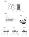
- Fig. 1 is a schematic explanation view showing a principle of dispersing electroplating.
- Fine carbon fibers 10, e.g., CNTs, or derivatives of fine carbon fibers are uniformly dispersed in a plating solution by a dispersing agent.
- the plating solution is agitated during the plating process, so that the fine carbon fibers 10, etc. are capable of swimming in the plating solution without settling down.
- the fine carbon fibers 10, etc. which locate on the surface of the substrate 12, are incorporated in a plating film 14 by electrolytic plating, so that a composite material (plating structure) of the metal and the fine carbon fibers, etc. is formed on the surface of the substrate 12.
- the plating method is not limited to a direct current plating method, further a current inversion plating method, a pulse plating method, etc. may be employed.
- the fine carbon fibers 10 has slight water repellency, and they are hard to be dispersed in the plating solution without the dispersing agent. Especially, fluorinated carbon fibers are very hard to be dispersed.
- the dispersing agent is added to the plating solution so as to disperse the fine carbon fibers, etc. therein.
- the dispersing agent is not limited, but cationic or nonionic surface acting agents (surfactant) can be used as preferred dispersing agents for electrolytic plating.
- Preferred cationic surface acting agents are, for example, cetyltrimethylammonium chloride, cetyltrimethylammonium bromide, cetylpyridinium chloride.
- cationic surface acting agents e.g., N -[(3-perfluorooctanesulfonamide) propyl]- N,N,N ,-trimethylammonium iodide, may be used.
- Preferred anionic surface acting agents are, for example, sodium dedocyl sulfate, dodecanoic sodium, sodium tetradecylsulfate, fatty acid sodium, fatty triethanolamine salt, sodium alkylbenzenesulfate, sodium monoalkyl phosphate.
- anionic surface acting agents e.g., perfluorooctane sulfonic acid, perfluorooctane sulfonate, N-propyl-N-perfluorooctylsulfonyl glycine potassium salt, bis[2-(N-propyl perfluorooctylsulfonylamino)ethyl] ammonium phosphate, perfluorocaprylic acid, perfluorooctanoate ammonium, may be used.
- Preferred nonionic surface acting agents are, for example, polyacrylic acid, polyethylene glycol, polyoxyethylene nonylphenyl ether, polyoxythylene dodecyl ether, polyoxyethylene lauryl ether, polyoxyethylene lauryl ether, polyoxyethylene fatty acidic ether, polyoxyethylene polyoxypropylene block polymer, polyoxyethylene alkylamine, alkylpolyglucoside, glycerin fatty acidic ester, sorbitan fatty acidic ester, saccharate fatty acidic ester, propylene glycol fatty acidic ester.
- nonionic surface acting agents e.g., N-Propyl-N-(2-hydroethyl) perfuorooctane sulfonate amide, N-polyoxyethylene-N-propylperfluorooctanesulfonate amide, N-(2-hydoroxyethylene)-N- perfluorooctylsulfonyl benzylamine, may be used.
- the surface acting agents may be solely used or combined.
- polycarboxylic acid e.g., polyacrylic acid
- salt thereof are suitable dispersing agents.
- Polyacrylic acid having molecular weight of about 3000-4000 has high uniform dispersibility.
- the plating solution is not limited, but nickel plating solution and copper plating solution are suitable solutions.
- Plating may be performed by not only electrolytic plating but also electroless plating.
- the plating structures produced by above described methods also have high heat conductivity and high electric conductivity. Therefore, they may be widely used, e.g., heat sinks, electric elements.
- the fine carbon fibers 10 are fixed in the plating film 14, and their ends project from a surface of the plating film 14. Especially, the state shown in Fig. 2 is remarkable in the plating film 14 plated with copper.
- the plating structure in which the fine carbon fibers 10 are fixed in the plating film 14 and their ends project therefrom as shown in Fig. 2, is suitably used as an emitter for field emission.
- CNTs carbon nano tubes
- CNTs have the great aspect ratio and the sharp ends, and they are chemically stable,mechanically tough and highly stable at high temperature, namely they are suitable materials of the emitter for field emission.
- CNTs have been used for a broad cold cathode of a light emitting device, in which a plurality of CNTs are fixed on a substrate and headed in the same direction by screen printing, etc..
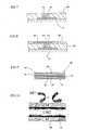
- Figs. 3-5 show steps of producing a fine mechanical part.
- a resist pattern 16 having a concave section 17 is formed on the substrate 12 by photolithography.
- a plating structure 18, in which the fine carbon fibers 10 are incorporated, is formed in the concave section 17, then the resist pattern 16 is removed as shown in Fig. 5, so that the pillar-shaped plating structure 18 is produced on the substrate 12.
- the plating structure 18 is removed from the substrate 12, so that fine mechanical parts, e.g., very fine gears 20 shown in Fig. 6, can be produced. Since the plating structure 18 (20) includes the fine carbon fibers, it can be used as, for example, a pillar shaped part having high toughness and high durability.
- Figs. 7 and 8 show steps of producing a multilayer circuit board, which is an example of electronic parts.
- an insulating layer 22 is formed on a cable pattern 21 of a lower layer by, for example, applying insulating resin; next, a via hole 23, in which the cable pattern 21 is exposed, is formed in the insulating layer 22 by, for example, laser means; and a plating structure (via) 24, in which fine carbon fibers are incorporated, is formed in the via hole 23 by the above described plating method.
- the multilayer circuit board which has the cable patterns constituted by the plating structures including the fine carbon fibers, can be produced.
- the plating method is not limited to the additive method; for example, the plating film (the plating structure) may be entirely formed on the insulating layer by electroless plating and electrolytic plating, then the plating film may be etched so as to form the cable pattern (a subtractive method).
- a cable pattern connected to electrodes of a semiconductor chip is a cable pattern connected to electrodes of a semiconductor chip, and the cable pattern may be produced by forming a polyimide resin layer (an insulating layer) on the semiconductor chip and forming the plating structure, which includes fine carbon fibers, thereon as the cable pattern. Bumps for connecting to an external circuit may be provided to proper positions so as to relocate the electrodes of the semiconductor chip.
- the cable pattern for relocating the electrodes has not only high electric conductivity but also high heat conductivity; the cable pattern acts as a heat sink of the semiconductor chip, and heat radiation rate thereof can be improved.
- Fig. 9 shows a heat radiator constituted by the plating structure.
- the multilayer body heat conductivity in a direction of piling the layers is different from that in an orthogonal direction (a direction parallel to each layer), so that the multilayered body can be used as an anisotropic heat conductor.
- the plated layers 32 include no fine carbon fibers, heat conductivity of the plated layers 31 including the fine carbon fibers is greater, so that the multilayer body is suitably used as the anisotropic heat conductor.
- the plated layers of the multilayer body may be made of three different metals or more.
- a plurality of the plated layers 31 constituted by the plated structure including the fine carbon fibers are arranged parallel with fine separations, so that a heat radiator 30 can be produced.
- the plated layers 31 have very high heat radiation rate, and total surface area of the plated layers 31, which are arranged parallel, is very large so that the heat radiator 30 has very high heat radiation rate.
- Fluorinated carbon fibers are produced by fluorinating fine carbon fibers, e.g., CNTs.
- the fluorination is performed under the following conditions.
- the fluorination is performed by the steps of: filling a nickel boat with fine carbon fibers (e.g., CNTs); setting in a nickel tube for fluorination; and reacting with fluorine for 72 hours at temperature of 340°C with fluorine-partial pressure of 460 mmHg and nitrogen-partial pressure of 310 mmHg, so that fluorinated carbon fibers, each of which has a structure of C x F y , can be produced.
- a nickel boat with fine carbon fibers e.g., CNTs
- a catalytic agent e.g., silver fluoride
- a catalytic agent e.g., silver fluoride
- the fluorinated carbon fibers have high water repellency.
- the fluorinated carbon fibers are added to a plating solution together with a dispersing agent, as well as the former embodiment, so as to uniformly disperse in the plating solution, then plating is performed with agitating the plating solution; the fluorinated carbon fibers, which locate on the surface of the substrate 12, are incorporated in the plating film 14 when the plating metal deposits onto the surface of the substrate 12 as well as the embodiment shown in Fig. 1, so that a composite material (plating structure) of the metal and the fluorinated carbon fibers is formed on the surface of the substrate 12.
- the composite material also has high water repellency.
- the plating is performed in the plating solution in which fine resin powders or fine resin fibers, e.g., fluorocarbon resin such as Teflon (trademark), is further dispersed,
- the fine resin powders or the fine resin fibers can be incorporated in the plating film together with the fluorinated carbon fibers.
- the composite material including the three substances also has high water repellency.
- the composite material including three substances may include the above described fine carbon fibers instead of the fluorinated carbon fibers.
- Fig. 10 shows the fine carbon fiber (CNT) 10, whose surface is coated with a plating film 34.
- the plating films 34 are formed by dispersing CNTs in a plating solution for electroless plating with a dispersing agent and performing electroless plating. By dispersing the CNTs 10 in the plating solution, the electroless plating films 34 can be formed on surfaces of the CNTs 10 with uniform thickness.
- the carbon fibers whose surfaces are coated with the plating films, have great specific gravity, and they have high homology with metals; the carbon fibers can be uniformly dispersed in a molten metal, so that a composite material, in which the carbon fibers and the metal are well homogenized, can be produced. And, the carbon fibers may be dispersed in resin so as to produce a composite material including the resin. Further, the carbon fibers, whose surfaces are coated with the plating films, may be mixed with adhesive resin so as to produce electric conductive resin.
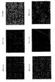
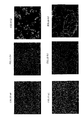
- Plating films were respectively formed in the Base Solution 1 and the plating solutions of Examples 1 and 2, which were agitated while plating, by electrolytic plating with current density of 2A/dm 2 , and micrographs of their surfaces taken by a scanning electron microscope (SEM) are shown in Figs. 11(a), (a'), Figs. 11(b), (b') and Figs. 11(c), (c') (note that, (a'), (b') and (c') are enlarged views of (a), (b) and (c). The relations in the following Examples are the same as here). Figs. 12(a) and (b) are enlarged views of Fig. 11(c'), whose rate of enlargement are different.
- a surface of a nickel plating film was relatively rough; as clearly shown in Figs. 11(b) and 11(b'), flatness of the surface was improved and a lustered plating film was gained by adding polyacrylic acid.
- Polyacrylic acid acted as not only the agent for dispersing CNTs but also a brightening agent.
- the CNTs were incorporated in the nickel plating film.
- nickel grew on surfaces of the CNTs like particles and covered the CNTs, further the particles of nickel were joined each other, so that the CNTs were incorporated in the nickel plating film.
- Example 3 Base Solution 1 + PA25000 2 ⁇ 10 -4 M (Example 4) Base Solution 1 + PA25000 2 ⁇ 10 -4 M CNT 2 g/l (Note that, PA25000 was polyacrylic acid, whose molecular weight was 25000)
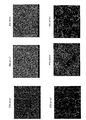
- Plating films were respectively formed in the Base Solution 1 and the plating solutions of Examples 3 and 4, which were agitated while plating, by electrolytic plating with current density of 2A/dm 2 , and micrographs of their surfaces taken by the scanning electron microscope (SEM) are shown in Figs. 15(a), (a'), Figs. 15(b), (b') and Figs. 15(c), (c').
- Figs. 16(a) and (b) are enlarged views of Fig. 15(c'), whose rate of enlargement are different.
- the molecular weight of polyacrylic acid was 25000, but results were almost the same as those shown in Figs. 11.
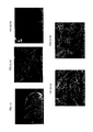
- Plating films were respectively formed in the Base Solution 2 and the plating solutions of Examples 5 and 6, which were agitated while plating, by electrolytic plating with current density of 2A/dm 2 , and micrographs of their surfaces taken by the scanning electron microscope (SEM) are shown in Figs. 17(a), (a'), Figs. 17(b), (b') and Figs. 17(c), (c').
- Fig. 19 is an enlarged view of Fig. 18(c'). As clearly shown in Figs. 18(a) and 18(a'), a surface of a copper plating film was rough; as clearly shown in Figs.
- Plating films were respectively formed in the Base Solution 2 and the plating solutions of Examples 7 and 8, which were agitated while plating, by electrolytic plating with current density of 2A/dm 2 , and micrographs of their surfaces taken by the scanning electron microscope (SEM) are shown in Figs. 20(a), (a'), Figs. 20(b), (b') and Figs. 20(c), (c').
- Figs. 22(a) and (b) are enlarged views of Fig. 21(c'), whose rate of enlargement are different.
- a surface of a copper plating film was relatively rough; as clearly shown in Figs.
- PA5000 of 2 ⁇ 10 -5 M was added to fine carbon fibers (VGCF: tradename) of 0.2g/l, and the VGCFs were dispersed in pure water by supersonic waves, then the mixture was filtered with filter paper, further the filtered substances were soaked in a HCl solution of 10g/l and SnCl 2 +10ml/l for 5 minutes at temperature of 25°C and further filtered. The filtered substances were treated in a HCl solution of 10mg/l and PdCl 2 +10ml/l for 5 minutes at temperature of 25°C and filtered.
- the filtered substances were electroless-plated for 15 minutes in an electroless nickel plating solution (a pH value was adjusted to nine by adding ammonia) having the following composition at temperature of 35°C. H 2 SO 4 20g/l sodium hypophosphite 20g/l sodium citrate 20g/l
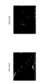
- FIG. 23 Micrographs of the VGCFs taken by the scanning electron microscope (SEM) are shown in Fig. 23, which show the fibers not plated (Fig. 23(a)) and those electroless-plated with nickel (Fig. 23(b)). According to the drawings, surfaces of the VGCFs were coated with electroless-plating nickel films.
- the present invention is capable of providing a plating structure, in which fine carbon fibers or derivatives thereof are incorporated in a plating metal, and a method of producing said plating structure.
Landscapes
- Chemical & Material Sciences (AREA)
- Metallurgy (AREA)
- Chemical Kinetics & Catalysis (AREA)
- Engineering & Computer Science (AREA)
- Materials Engineering (AREA)
- Organic Chemistry (AREA)
- Mechanical Engineering (AREA)
- General Chemical & Material Sciences (AREA)
- Electrochemistry (AREA)
- Dispersion Chemistry (AREA)
- Electroplating Methods And Accessories (AREA)
- Chemically Coating (AREA)
- Cooling Or The Like Of Semiconductors Or Solid State Devices (AREA)
- Cold Cathode And The Manufacture (AREA)
- Manufacturing Of Printed Wiring (AREA)
Applications Claiming Priority (3)
| Application Number | Priority Date | Filing Date | Title |
|---|---|---|---|
| JP2002320407 | 2002-11-01 | ||
| JP2002320407A JP4032116B2 (ja) | 2002-11-01 | 2002-11-01 | 電子部品およびその製造方法 |
| PCT/JP2003/013893 WO2004040044A1 (ja) | 2002-11-01 | 2003-10-29 | めっき構造物とその製造方法 |
Publications (2)
| Publication Number | Publication Date |
|---|---|
| EP1564314A1 true EP1564314A1 (de) | 2005-08-17 |
| EP1564314A4 EP1564314A4 (de) | 2006-07-12 |
Family
ID=32211853
Family Applications (1)
| Application Number | Title | Priority Date | Filing Date |
|---|---|---|---|
| EP03769999A Withdrawn EP1564314A4 (de) | 2002-11-01 | 2003-10-29 | Metallüberzugsstruktur und herstellungsverfahren dafür |
Country Status (7)
| Country | Link |
|---|---|
| US (1) | US20060099438A1 (de) |
| EP (1) | EP1564314A4 (de) |
| JP (1) | JP4032116B2 (de) |
| KR (1) | KR101066751B1 (de) |
| CN (1) | CN100523310C (de) |
| AU (1) | AU2003280624A1 (de) |
| WO (1) | WO2004040044A1 (de) |
Cited By (4)
| Publication number | Priority date | Publication date | Assignee | Title |
|---|---|---|---|---|
| WO2007071542A1 (de) * | 2005-12-19 | 2007-06-28 | Siemens Aktiengesellschaft | Beschichtung für eine kokille für eine stranggiessanlage und verfahren zur beschichtung |
| WO2008155284A1 (de) * | 2007-06-19 | 2008-12-24 | Siemens Aktiengesellschaft | Kokillenplatte für eine kokille einer stranggiessanlage |
| WO2010021629A1 (en) * | 2008-08-22 | 2010-02-25 | E. I. Du Pont De Nemours And Company | Method for the electrochemical deposition of carbon nanotubes |
| IT201700012608A1 (it) * | 2017-02-06 | 2018-08-06 | Arnaldo Morganti | Componenti meccanici antifrizione perfezionati, procedimento di rivestimento e vasca dell’impianto per la loro fabbricazione |
Families Citing this family (46)
| Publication number | Priority date | Publication date | Assignee | Title |
|---|---|---|---|---|
| WO2004051726A1 (ja) * | 2002-11-29 | 2004-06-17 | Nec Corporation | 半導体装置およびその製造方法 |
| JP4689218B2 (ja) * | 2003-09-12 | 2011-05-25 | 株式会社半導体エネルギー研究所 | 半導体装置の作製方法 |
| JP2005277096A (ja) * | 2004-03-24 | 2005-10-06 | Japan Science & Technology Agency | カーボンナノチューブ含有金属膜を用いてなる半導体配線とその製造方法、およびカーボンナノチューブ含有金属膜の製造方法 |
| KR100593907B1 (ko) * | 2004-05-21 | 2006-06-30 | 삼성전기주식회사 | 전계방출 에미터전극 제조방법 및 이를 이용하여 제조된전계방출장치 |
| JP4697857B2 (ja) * | 2004-07-20 | 2011-06-08 | 株式会社リコー | インクジェットヘッド及びインクジェット記録装置 |
| JP2006080170A (ja) | 2004-09-08 | 2006-03-23 | Hitachi Cable Ltd | Cnt入り配線材の製造方法およびスパッタリング用ターゲット材 |
| US7906210B2 (en) | 2004-10-27 | 2011-03-15 | Nissei Plastic Industrial Co., Ltd. | Fibrous nanocarbon and metal composite and a method of manufacturing the same |
| KR100638668B1 (ko) * | 2005-01-07 | 2006-10-30 | 삼성전기주식회사 | 전계방출 에미터 어레이 및 그 제조 방법 |
| DE102005006982A1 (de) * | 2005-02-15 | 2006-08-17 | Basf Ag | Verwendung nichtionischer Tenside bei der Metallgewinnung durch Elektrolyse |
| JP4716760B2 (ja) * | 2005-03-09 | 2011-07-06 | 国立大学法人信州大学 | 金めっき液および金めっき方法 |
| JP2006265667A (ja) * | 2005-03-24 | 2006-10-05 | Totoku Electric Co Ltd | カーボン複合めっき電線及びその製造方法 |
| KR100688860B1 (ko) * | 2005-08-08 | 2007-03-02 | 삼성전기주식회사 | 전계방출소자의 제조 방법 |
| JP2007070689A (ja) * | 2005-09-07 | 2007-03-22 | Nissan Motor Co Ltd | ナノカーボン/アルミニウム複合材、その製造方法及びこれに用いるめっき液 |
| US8845866B2 (en) | 2005-12-22 | 2014-09-30 | General Electric Company | Optoelectronic devices having electrode films and methods and system for manufacturing the same |
| CN100564610C (zh) * | 2006-03-09 | 2009-12-02 | 上海交通大学 | 电沉积制备定向短纤维增强金属基复合材料的方法 |
| JP2008028200A (ja) * | 2006-07-21 | 2008-02-07 | Matsushita Electric Works Ltd | 立体回路部品およびその製造方法 |
| WO2008129525A1 (en) * | 2007-04-23 | 2008-10-30 | University College Cork - National University Of Ireland, Cork | A thermal interface material |
| JP5031450B2 (ja) * | 2007-06-12 | 2012-09-19 | 富士フイルム株式会社 | 複合圧電材料、超音波探触子、超音波内視鏡、及び、超音波診断装置 |
| WO2009075320A1 (ja) * | 2007-12-11 | 2009-06-18 | Sumitomo Electric Industries, Ltd. | 冷却デバイスとその製造方法 |
| JP2009210552A (ja) * | 2008-02-07 | 2009-09-17 | Seiko Epson Corp | 接触部品および時計 |
| JP5389455B2 (ja) * | 2008-02-21 | 2014-01-15 | セイコーインスツル株式会社 | 摺動部品及び時計 |
| JP2010027916A (ja) * | 2008-07-22 | 2010-02-04 | Meiko:Kk | プリント配線板 |
| JP5266088B2 (ja) * | 2009-02-18 | 2013-08-21 | パナソニック株式会社 | 電磁シールド用めっき膜、電磁シールド基板及びその製造方法 |
| TW201041009A (en) * | 2009-05-08 | 2010-11-16 | Univ Nat Taiwan Science Tech | Fabrication method of carbon nanotube field emission cathode |
| JP5334052B2 (ja) * | 2009-06-11 | 2013-11-06 | 独立行政法人産業技術総合研究所 | 構造部材およびその製造方法 |
| WO2011048984A1 (ja) * | 2009-10-19 | 2011-04-28 | 株式会社 村田製作所 | めっき浴の作製方法、めっき浴、及び電子部品 |
| KR101217507B1 (ko) * | 2009-11-12 | 2013-01-02 | 한국기계연구원 | 패턴이 구비된 복합재료의 제조방법 |
| KR101161060B1 (ko) * | 2009-11-30 | 2012-06-29 | 서강대학교산학협력단 | 나노입자를 기둥형태로 조직화시키기 위한 배열장치 및 그 배열방법 |
| JP5631775B2 (ja) * | 2011-02-24 | 2014-11-26 | 新光電気工業株式会社 | 複合めっき液 |
| US8853540B2 (en) * | 2011-04-19 | 2014-10-07 | Commscope, Inc. Of North Carolina | Carbon nanotube enhanced conductors for communications cables and related communications cables and methods |
| KR20140036293A (ko) | 2011-06-03 | 2014-03-25 | 파나소닉 주식회사 | 전기 접점 부품 |
| US20130126212A1 (en) * | 2011-11-22 | 2013-05-23 | Tyco Electronica Corporation | Conductive members using carbon-based substrate coatings |
| JP6127289B2 (ja) * | 2012-03-02 | 2017-05-17 | 国立大学法人信州大学 | リチウムイオン電池用負極材料およびその製造方法 |
| JP6118540B2 (ja) | 2012-11-08 | 2017-04-19 | 新光電気工業株式会社 | 放熱部品及びその製造方法 |
| JP6304681B2 (ja) * | 2013-07-24 | 2018-04-04 | 国立大学法人信州大学 | 金属膜及び金属膜の形成方法 |
| JP6483616B2 (ja) * | 2013-10-08 | 2019-03-13 | 日本ゼオン株式会社 | 金属複合材料の製造方法 |
| JP2016012799A (ja) | 2014-06-27 | 2016-01-21 | Tdk株式会社 | 高周波伝送線路、アンテナ及び電子回路基板 |
| JP2016012798A (ja) | 2014-06-27 | 2016-01-21 | Tdk株式会社 | 高周波伝送線路、アンテナ及び電子回路基板 |
| JP6558769B2 (ja) * | 2014-09-09 | 2019-08-14 | 国立大学法人信州大学 | Sn系金属を保持する銅三次元ナノ構造体の製造方法 |
| CN107923059A (zh) * | 2015-08-28 | 2018-04-17 | 日本瑞翁株式会社 | 复合材料的制造方法及复合材料 |
| JP6536819B2 (ja) * | 2015-12-03 | 2019-07-03 | トヨタ自動車株式会社 | 銅皮膜の成膜方法 |
| US10316424B2 (en) | 2016-02-23 | 2019-06-11 | Samsung Electronics Co., Ltd. | Flexible electrically conductive structure, flexible wiring board, production method thereof, and electronic device includng the same |
| WO2018051925A1 (ja) * | 2016-09-16 | 2018-03-22 | 日本ゼオン株式会社 | 複合体およびリチウムイオン二次電池用負極、並びに複合体の製造方法 |
| CN107099834A (zh) * | 2017-03-29 | 2017-08-29 | 广东工业大学 | 一种铜基自润滑复合涂层及其制备方法 |
| CN107099833A (zh) * | 2017-03-29 | 2017-08-29 | 广东工业大学 | 一种复合电镀液及其制备方法 |
| DE102023103001A1 (de) * | 2023-02-08 | 2024-08-08 | Te Connectivity Solutions Gmbh | Selbstschmierende Beschichtung, Verfahren zu deren Herstellung und elektrischer Kontakt |
Family Cites Families (8)
| Publication number | Priority date | Publication date | Assignee | Title |
|---|---|---|---|---|
| JPS5468727A (en) | 1977-11-11 | 1979-06-02 | Nippon Carbon Co Ltd | Manufacture of carbon fiber-metal composite material |
| JPS61221394A (ja) * | 1985-03-27 | 1986-10-01 | C Uyemura & Co Ltd | 電気めつき方法 |
| JPH04158932A (ja) * | 1990-10-19 | 1992-06-02 | Eagle Ind Co Ltd | ベローズの製造方法 |
| JP3306606B2 (ja) * | 1993-05-14 | 2002-07-24 | 大阪瓦斯株式会社 | 高耐久性・高撥水性複合メッキ被膜を備えた基板材およびその製造法ならびに製氷板 |
| JP3730476B2 (ja) * | 2000-03-31 | 2006-01-05 | 株式会社東芝 | 電界放出型冷陰極及びその製造方法 |
| JP2002150922A (ja) * | 2000-08-31 | 2002-05-24 | Sony Corp | 電子放出装置、冷陰極電界電子放出素子及びその製造方法、並びに、冷陰極電界電子放出表示装置及びその製造方法 |
| JP2002088482A (ja) * | 2000-09-14 | 2002-03-27 | Japan Science & Technology Corp | 分散材磁場めっき方法と分散材磁場共析めっき方法 |
| CN1132968C (zh) * | 2001-12-20 | 2003-12-31 | 上海交通大学 | 镍基复合材料复合电铸制备方法 |
-
2002
- 2002-11-01 JP JP2002320407A patent/JP4032116B2/ja not_active Expired - Lifetime
-
2003
- 2003-10-29 AU AU2003280624A patent/AU2003280624A1/en not_active Abandoned
- 2003-10-29 US US10/532,940 patent/US20060099438A1/en not_active Abandoned
- 2003-10-29 EP EP03769999A patent/EP1564314A4/de not_active Withdrawn
- 2003-10-29 WO PCT/JP2003/013893 patent/WO2004040044A1/ja not_active Ceased
- 2003-10-29 CN CNB2003801049138A patent/CN100523310C/zh not_active Expired - Fee Related
- 2003-10-29 KR KR1020057007377A patent/KR101066751B1/ko not_active Expired - Fee Related
Cited By (4)
| Publication number | Priority date | Publication date | Assignee | Title |
|---|---|---|---|---|
| WO2007071542A1 (de) * | 2005-12-19 | 2007-06-28 | Siemens Aktiengesellschaft | Beschichtung für eine kokille für eine stranggiessanlage und verfahren zur beschichtung |
| WO2008155284A1 (de) * | 2007-06-19 | 2008-12-24 | Siemens Aktiengesellschaft | Kokillenplatte für eine kokille einer stranggiessanlage |
| WO2010021629A1 (en) * | 2008-08-22 | 2010-02-25 | E. I. Du Pont De Nemours And Company | Method for the electrochemical deposition of carbon nanotubes |
| IT201700012608A1 (it) * | 2017-02-06 | 2018-08-06 | Arnaldo Morganti | Componenti meccanici antifrizione perfezionati, procedimento di rivestimento e vasca dell’impianto per la loro fabbricazione |
Also Published As
| Publication number | Publication date |
|---|---|
| WO2004040044A1 (ja) | 2004-05-13 |
| KR101066751B1 (ko) | 2011-09-21 |
| US20060099438A1 (en) | 2006-05-11 |
| CN100523310C (zh) | 2009-08-05 |
| AU2003280624A1 (en) | 2004-05-25 |
| KR20050083845A (ko) | 2005-08-26 |
| EP1564314A4 (de) | 2006-07-12 |
| JP2004156074A (ja) | 2004-06-03 |
| JP4032116B2 (ja) | 2008-01-16 |
| CN1720355A (zh) | 2006-01-11 |
Similar Documents
| Publication | Publication Date | Title |
|---|---|---|
| US20060099438A1 (en) | Metal plating structure and method for production thereof | |
| CN101622701B (zh) | 电子制造中的锡银焊接凸点 | |
| CN102650072B (zh) | 复合电镀液 | |
| CN108396346A (zh) | 一种石墨烯铜/钢复合材料的制备方法和应用 | |
| CN115142100B (zh) | 一种用于pcb通孔金属致密填充的酸性硫酸盐电子电镀铜组合添加剂 | |
| CN108866369B (zh) | 三维多孔复合材料 | |
| KR20130116061A (ko) | 환원 석출형 구형 NiP 미소입자 및 그의 제조 방법 | |
| JP4599565B2 (ja) | 電解めっき方法および電解めっき液 | |
| JP2021528573A (ja) | 積層構造体、それを含む軟性銅箔積層フィルム、及び該積層構造体の製造方法 | |
| JP2005332798A (ja) | 電界放出エミッタ電極の製造方法及びこれを利用して製造した電界放出装置 | |
| CN114059116A (zh) | 一种电沉积制备FeCoNiCuSn高熵合金的方法 | |
| JP2010001569A (ja) | 粒状物及びその製造方法 | |
| CN1219981A (zh) | 无电镀铜溶液和无电镀铜的方法 | |
| CN111194362A (zh) | 表面处理铜箔、以及使用其的覆铜板及印刷配线板 | |
| JP2010222707A (ja) | 無電解めっき方法および無電解めっき液 | |
| JP4392506B2 (ja) | 放熱体 | |
| CN1325790A (zh) | Tab带载体的铜箔以及使用铜箔的tab载体带和tab带载体 | |
| WO2004074550A1 (en) | ELECTROLYTE FOR NANOCRYSTALLINE Fe-Ni ALLOYS WITH LOW THERMAL EXPANSION | |
| KR20220071430A (ko) | 도금피막 내 은 함량의 분포 편차가 개선된 웨이퍼 범프용 주석-은 합금 전기 도금액 | |
| US20060043862A1 (en) | Method of manufacturing field emitter electrode using carbon nanotube nucleation sites and field emitter electrode manufactured thereby | |
| JP2007211305A (ja) | 複合電解銅箔およびその製造方法 | |
| JP2007182623A (ja) | 金属薄体の製造方法 | |
| JP2011058061A (ja) | 無電解Cuめっき液、無電解Cuめっき方法および無電解Cuめっき液へのCNT分散剤 | |
| JP2003298264A (ja) | 熱交換器 | |
| Choi et al. | Acid Palladium-Nickel Electroplating Using Ethylenediamine as Complexing Agent |
Legal Events
| Date | Code | Title | Description |
|---|---|---|---|
| PUAI | Public reference made under article 153(3) epc to a published international application that has entered the european phase |
Free format text: ORIGINAL CODE: 0009012 |
|
| 17P | Request for examination filed |
Effective date: 20050523 |
|
| AK | Designated contracting states |
Kind code of ref document: A1 Designated state(s): AT BE BG CH CY CZ DE DK EE ES FI FR GB GR HU IE IT LI LU MC NL PT RO SE SI SK TR |
|
| AX | Request for extension of the european patent |
Extension state: AL LT LV MK |
|
| DAX | Request for extension of the european patent (deleted) | ||
| RBV | Designated contracting states (corrected) |
Designated state(s): DE FR |
|
| A4 | Supplementary search report drawn up and despatched |
Effective date: 20060612 |
|
| 17Q | First examination report despatched |
Effective date: 20080925 |
|
| STAA | Information on the status of an ep patent application or granted ep patent |
Free format text: STATUS: THE APPLICATION IS DEEMED TO BE WITHDRAWN |
|
| 18D | Application deemed to be withdrawn |
Effective date: 20130502 |