EP1564750A2 - Mémoire d'accès aléatoire magnétique et procédé de lecture correspondant - Google Patents
Mémoire d'accès aléatoire magnétique et procédé de lecture correspondant Download PDFInfo
- Publication number
- EP1564750A2 EP1564750A2 EP04258119A EP04258119A EP1564750A2 EP 1564750 A2 EP1564750 A2 EP 1564750A2 EP 04258119 A EP04258119 A EP 04258119A EP 04258119 A EP04258119 A EP 04258119A EP 1564750 A2 EP1564750 A2 EP 1564750A2
- Authority
- EP
- European Patent Office
- Prior art keywords
- cell
- memory cell
- mtj
- transistor
- reference cell
- Prior art date
- Legal status (The legal status is an assumption and is not a legal conclusion. Google has not performed a legal analysis and makes no representation as to the accuracy of the status listed.)
- Granted
Links
Images


Classifications
-
- G—PHYSICS
- G11—INFORMATION STORAGE
- G11C—STATIC STORES
- G11C11/00—Digital stores characterised by the use of particular electric or magnetic storage elements; Storage elements therefor
- G11C11/02—Digital stores characterised by the use of particular electric or magnetic storage elements; Storage elements therefor using magnetic elements
- G11C11/16—Digital stores characterised by the use of particular electric or magnetic storage elements; Storage elements therefor using magnetic elements using elements in which the storage effect is based on magnetic spin effect
-
- G—PHYSICS
- G11—INFORMATION STORAGE
- G11C—STATIC STORES
- G11C11/00—Digital stores characterised by the use of particular electric or magnetic storage elements; Storage elements therefor
- G11C11/02—Digital stores characterised by the use of particular electric or magnetic storage elements; Storage elements therefor using magnetic elements
- G11C11/14—Digital stores characterised by the use of particular electric or magnetic storage elements; Storage elements therefor using magnetic elements using thin-film elements
- G11C11/15—Digital stores characterised by the use of particular electric or magnetic storage elements; Storage elements therefor using magnetic elements using thin-film elements using multiple magnetic layers
-
- G—PHYSICS
- G11—INFORMATION STORAGE
- G11C—STATIC STORES
- G11C11/00—Digital stores characterised by the use of particular electric or magnetic storage elements; Storage elements therefor
- G11C11/02—Digital stores characterised by the use of particular electric or magnetic storage elements; Storage elements therefor using magnetic elements
- G11C11/16—Digital stores characterised by the use of particular electric or magnetic storage elements; Storage elements therefor using magnetic elements using elements in which the storage effect is based on magnetic spin effect
- G11C11/165—Auxiliary circuits
- G11C11/1659—Cell access
-
- G—PHYSICS
- G11—INFORMATION STORAGE
- G11C—STATIC STORES
- G11C11/00—Digital stores characterised by the use of particular electric or magnetic storage elements; Storage elements therefor
- G11C11/02—Digital stores characterised by the use of particular electric or magnetic storage elements; Storage elements therefor using magnetic elements
- G11C11/16—Digital stores characterised by the use of particular electric or magnetic storage elements; Storage elements therefor using magnetic elements using elements in which the storage effect is based on magnetic spin effect
- G11C11/165—Auxiliary circuits
- G11C11/1673—Reading or sensing circuits or methods
-
- G—PHYSICS
- G11—INFORMATION STORAGE
- G11C—STATIC STORES
- G11C7/00—Arrangements for writing information into, or reading information out from, a digital store
- G11C7/06—Sense amplifiers; Associated circuits, e.g. timing or triggering circuits
- G11C7/062—Differential amplifiers of non-latching type, e.g. comparators, long-tailed pairs
-
- G—PHYSICS
- G11—INFORMATION STORAGE
- G11C—STATIC STORES
- G11C7/00—Arrangements for writing information into, or reading information out from, a digital store
- G11C7/14—Dummy cell management; Sense reference voltage generators
Definitions
- the present invention relates to a semiconductor memory device, and more particularly, to a magnetic random access memory (MRAM) having a reference cell for maintaining a middle resistance between a high resistance and a low resistance of a magnetic tunneling junction (MTJ) layer according to changes in a resistance of the MTJ layer caused by an applied voltage and a method of reading data from the MRAM.
- MRAM magnetic random access memory
- MTJ magnetic tunneling junction
- a magnetic tunneling junction (MTJ) layer of a memory cell of an MRAM has a resistance that varies according to the direction of magnetization of a free magnetic film.
- the MTJ layer has a low resistance R L .
- the MTJ layer has a high resistance R H .
- the high resistance is referred to as a maximum resistance of the MTJ layer, and the low resistance is referred to as a minimum resistance of the MTJ layer.
- the MRAM is a memory device that stores data 1 and 0 using the fact that the resistance of the MTJ layer is different according to the state of magnetization of the free magnetic film.
- the MRAM includes a reference cell having a resistance (R H +R L )/2 (hereinafter, referred to as a middle resistance) which corresponds to a middle between the high resistance R H and the low resistance R L of the MTJ layer.
- the reference cell includes a transistor and a MTJ layer connected to the transistor.
- the middle resistance of the reference cell is the resistance of the MTJ layer provided in the reference cell.
- the resistances R H and R L of the MTJ layer vary according to a voltage applied to the MTJ layer.
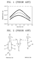
- the resistance represented by solid line of the MTJ layer of the reference cell of the MRAM should be constant to be a middle resistance (R H +R L )/2 between a low resistance R L ( ⁇ ) and a high resistance R H ( ⁇ ) of the MTJ layer of the memory cell according to a voltage applied to the reference cell.
- the reference cell of the MRAM by the prior art comprises first through fourth MTJ layers 12, 14, 16, and 18 and a first transistor 10, as shown in the left side of FIG. 2.
- a memory cell comprising a fifth MTJ layer 20 and a second transistor 24 is shown on the right side of a sensor amplifier SA of FIG. 2.
- a resistance is measured from the MTJ layer. Accordingly, in FIG. 2, the MTJ layer is indicated by a resistance. Hereinafter, the MTJ layer in all circuits is indicated by a resistance.
- the first and second MTJ layers 12 and 14 have a high resistance R H and a low resistance R L , respectively.
- the third and fourth MTJ layers 16 and 18 have a low resistance R L and a high resistance R H , respectively.
- the first and second MTJ layers 12 and 14 are connected in series to each other, and the third and fourth MTJ layers 16 and 18 are also connected in series to each other.
- the first and second MTJ layers 12 and 14 and the third and fourth MTJ layers 16 and 18 are connected in parallel to each other.
- the first transistor 10 is connected between the second and fourth MTJ layers 14 and 18.
- V Ref and V Cell are a voltage measured in the reference cell and a voltage measured in the memory cell, respectively.
- a conventional MRAM comprising the reference cell and the memory cell shown in FIG. 2 reads information stored in the memory cell using a difference between the voltages V Ref and V Cell .
- the current l s supplied to the reference cell from a current source is divided into two such that a current l s /2 is supplied to each of the first and second MTJ layers 12 and 14 and the third and fourth MTJ layers 16 and 18.
- the voltage applied to each MTJ layer of the reference cell is about the half of the voltage applied to the fifth MTJ layer 20 of the memory cell. For this reason, it is difficult to maintain the equivalent resistance of the reference cell at (R H +R L )/2, as shown in FIG. 3.
- a reference diagram • is a graph showing a voltage V Cell ,H measured when the fifth MTJ layer 20 has a high resistance
- a reference diagram ⁇ is a graph showing a voltage V Cell ,L measured when the fifth MTJ layer 20 has a low resistance
- a solid line (-) is a graph showing a voltage V Ref measured in the reference cell. Referring to the graphs, the voltage V Ref measured in the reference cell is different from (V Cell ,H + V Cell ,L)/2.
- the voltage measured in the reference cell does not have a middle value between a maximum voltage and a minimum voltage measured in the memory cell in this way, in case of the conventional MRAM having the memory cell and the reference cell of FIG. 2, a sensing margin is reduced such that noise or malfunction may occur.
- the reference cell and the memory cell of FIG. 5 are the same as the reference cell and the memory cell of FIG. 2 in constitution, but there is a difference between FIGS. 5 and 2 in that a voltage instead of a current is applied to the reference cell and the memory cell.
- an MRAM having the reference cell and the memory cell of FIG. 5 reads information recorded in the memory cell using a difference between a current I Ref measured in the reference cell and a current I Cell measured in the memory cell.
- voltages applied to each of the first through fourth MTJ layers 12, 14, 16, and 18 of the reference cell is small to be about the half of a voltage applied to the fifth MTJ layer 20 of the memory cell.
- a reference diagram • is a graph showing maximum currents I Cell ,H measured in the memory cell
- a reference diagram ⁇ is a graph showing minimum currents I Cell, L measured in the memory cell
- a solid line (-) is a graph showing a current l Ref measured in the reference cell.
- the current l Ref measured in the reference cell is very different from a middle value (I Cell ,H + I Cell ,L)/2 between the maximum currents I Cell, H and the minimum currents I Cell, L measured in the memory cell according to an applied voltage.
- FIG. 7 shows an MRAM having a reference cell comprising sixth and seventh MTJ layers 26 and 28, and the first transistor 10.
- the sixth MTJ layer 26 has a low resistance R L
- the seventh MTJ layer 28 has a resistance R H higher than the sixth MTJ layer 26.
- the sixth and seventh MTJ layers 26 and 28 are connected in parallel to each other, and the first transistor 10 is connected between the sixth and seventh MTJ layers 26 and 28.
- a voltage 0.5V s corresponding to 1/2 of a voltage V s supplied to the memory cell is applied to the reference cell.
- the voltage 0.5V s applied to the two MTJ layers 26 and 28 of the reference cell is about the half of the voltage V s applied to the fifth MTJ layer 20 of the memory cell, it is difficult to maintain the equivalent resistance of the reference cell at (R H +R L )/2.
- the current I Ref measured in the reference cell of the MRAM of FIG. 7 can not be maintained at a middle value (I Cell ,H + I Cell ,L)/2 between the maximum current I Cell ,H and the minimum current I Cell ,L measured in the memory cell, as shown in FIG. 6. For this reason, in case of the MRAM of FIG. 7, a sensing margin is reduced such that noise or malfunction may occur.
- an MRAM comprising a memory cell having one transistor and one magnetic tunneling junction (MTJ) layer and a reference cell which is used as a basis when reading data stored in the memory cell, wherein the reference cell comprises first and second MTJ layers provided in parallel to each other and first and second transistors provided in parallel to each other, the first and second transistors being respectively connected in serial to the first and second MTJ layers.
- MTJ magnetic tunneling junction
- a magnetic random access memory including a memory cell having one transistor and one magnetic tunneling junction (MTJ) layer and a reference cell which is used as a basis when reading data stored in the memory cell, wherein the reference cell comprises first and second MTJ layers provided in parallel to each other and a first transistor connected in series to the first and second MTJ layers, and a driving capability of the first transistor is twice a driving capability of the transistor of the memory cell.
- MTJ magnetic tunneling junction
- a method of reading data from an MRAM comprising a memory cell having one transistor and one magnetic tunneling junction (MTJ) layer and a reference cell having first and second MTJ layers provided in parallel to each other and first and second transistors provided in parallel to each other, the first and second transistors being respectively connected in serial to the first and second MTJ layers, wherein a read current l s is applied to the memory cell and a current 2l s corresponding to twice the read current is applied to the reference cell.
- MTJ magnetic tunneling junction
- the present invention provides a magnetic random access memory (MRAM) capable of maintaining the equivalent resistance of a magnetic tunneling junction (MTJ) layer of a reference cell at a middle value (R H + R L )/2 between a maximum resistance R H and a minimum resistance R L of the MTJ layer of a memory cell even though an applied voltage varies.
- MRAM magnetic random access memory
- the present invention also provides a method of reading data from the M RAM.
- a method of reading data from an MRAM comprising a memory cell having one transistor and one magnetic tunneling junction (MTJ) layer and a reference cell having first and second MTJ layers connected in parallel to each other and a first transistor which is connected in series to the first and second MTJ layers and has a driving capability corresponding to twice a driving capability of the transistor of the memory cell, wherein a read current l s is applied to the memory cell and a current 2l s corresponding to twice the read current is applied to the reference cell.
- MTJ magnetic tunneling junction
- the equivalent resistance of the MTJ layer of the reference cell is maintained at the middle value between the maximum resistance and the minimum resistance of the MTJ layer of the memory cell even though the applied voltage varies such that a sensing margin can be sufficiently obtained and malfunction caused by noise can be prevented.
- MRAM magnetic random access memory
- a method of reading data from the MRAM according to an embodiment of the present invention will be described with reference to the accompanying drawings.
- thicknesses of layers or areas are exaggerated for clarity.
- FIG. 8 shows a circuit constitution for a memory cell C2 and a first reference cell C1 corresponding to the memory cell C2 of the MRAM according to an embodiment of the present invention.
- the first reference cell C1 includes first and second MTJ layers 50 and 52 and first and second transistors 54 and 56.
- the first MTJ layer 50 has a low resistance and may be the same as a minimum resistance of a third MTJ layer 58 of the memory cell C2.
- the second MTJ layer 52 of the first reference cell C1 has a resistance higher than the first MTJ layer 52.
- the resistance of the second MTJ layer 52 may be the same as a maximum resistance of the third MTJ layer 58.
- the above-described relation between the first and second MTJ layers 50 and 52 of the first reference cell C1 may be opposite.
- the first and second MTJ layers 50 and 52 of the first reference cell C1 are connected in parallel to each other, and the first and second transistors 54 and 56 are connected in parallel to each other.
- the first MTJ layer 50 and the first transistor 54 are connected in series to each other, and the second MTJ layer 52 and the second transistor 56 are also connected in series to each other.
- the memory cell C2 includes the third MTJ layer 58 and a third transistor 60.
- the first and second transistors 54 and 56 of the first reference cell C1 are the same as the third transistor 60 of the memory cell C2.
- a predetermined read current l s is applied to the memory cell C2 from a current source and simultaneously, a current 2l s corresponding to twice the read current l s is applied to the first reference cell C1, and voltages V Ref and V Cell respectively measured in the first reference cell C1 and the memory cell C2 are compared with each other such that data stored in the memory cell C2 is read.
- the current 2l s applied to the first reference cell C1 is branched so that the same current as the current l s applied to the memory cell C2 is applied to each of the first and second MTJ layers 50 and 52.
- the first and second transistors 54 and 56 which is the same as a pass transistor of the memory cell C2, that is, the third transistor 60, are respectively connected in series to the first and second MTJ layers 50 and 52 of the first reference cell C1, the voltage applied to the first and second MTJ layers 50 and 52 of the first reference cell C1 is very similar to the voltage applied to the third MTJ layer 58 of the memory cell C2.
- the equivalent resistance of the first reference cell C1 is maintained at a middle value between a maximum resistance R H and a minimum resistance R L of the third MTJ layer 58 of the memory cell C1 even though an applied voltage varies.
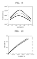
- FIG. 9 shows the result of the first reference cell C1.
- a reference diagram • shows changes in the maximum resistance of the third MTJ layer 58 of the memory cell C2 according to an applied voltage
- a reference diagram ⁇ shows changes in the minimum resistance of the third MTJ layer 58.
- a solid line (-) shows changes in the resistance measured in the first reference cell C1.
- the resistance measured in the first reference cell C1 is maintained at a middle value between the maximum resistance and the minimum resistance of the third MTJ layer 58 of the memory cell C2 even though the applied voltage varies.
- the voltage V Ref of the first reference cell C1 can be always maintained at a middle value (V Cell ,H + V Cell ,L)/2 between the maximum voltage V Cell ,H and the minimum voltage V Cell ,L of the memory cell C2 even though the applied voltage varies.
- FIG. 10 shows this result.
- a reference diagram • shows changes in the maximum resistance V Cell ,H of the memory cell C2 according to an applied voltage
- a reference diagram ⁇ shows changes in the minimum resistance V Cell ,L of the memory cell C2 according to the applied voltage.
- a solid line (-) shows changes in the resistance measured in the first reference cell C1 according to the applied voltage.
- the voltage of the first reference cell C1 is a middle value between the maximum voltage V Cell ,H and the minimum voltage V Cell ,L of the memory cell C2 in any applied voltage.
- a second reference cell comprising one transistor that substitutes for the first and second transistors 54 and 56 in the first reference cell C1 of FIG. 8 may exist.
- the one transistor is a pass transistor. Since a current that passes through two MTJ layers connected in parallel passes through the one substituted transistor, the driving capability of the one substituted transistor may be twice the driving capability of the third transistor 60 of the memory cell C2.
- a process of reading data from the memory cell C2 is the same as a process to be performed by the magnetic RAM comprising the first reference cell C1.
- each MTJ layer and the position of each transistor may be opposite in the first reference cell C1 of FIG. 8.
- FIG. 11 shows a cell array of an MRAM comprising the above-described second reference cell and memory cell.
- reference numeral 100 denotes a reference cell column having a plurality of second reference cells.
- One reference cell column 100 is disposed in each memory cell block.
- a current 2l s corresponding to twice a current l s applied to a memory cell column is applied to the reference cell column 100.
- One column of a memory cell block is selected by column select transistors Y0, Y1, Y2, and Y3 disposed under the cell array and is compared with the reference cell column 100.
- reference character DL denotes a digit line used in recording data in an MTJ layer of the memory cell. When a current is applied to the digit line DL, a ground line GL is floated so that a current does not flow through a pass transistor connected to the MTJ layer.
- FIG. 12 shows a path through which a current applied to a corresponding memory cell and the reference cell column 100 flows, so as to read data stored in a memory cell connected to a predetermined selected word line, for example, a first word line WLO, of the MRAM array of FIG. 11.
- a left circuit is a memory cell of a memory cell column to which a read current l s is applied and which is connected to the first word line WL0
- a right circuit is a second reference cell of the reference cell column 100 to which a current 2l s corresponding to twice the read current l s is applied and which is connected to the first word line WL0.
- the read current l s applied to the memory cell connected to the first word line WL0 passes through a MTJ layer 102 of the memory cell and a transistor MT1 connected in series to the MTJ layer 102 and flows through a ground line GL connected to the transistor MT1.
- the current 2l s applied to the reference cell column 100 is divided into two in a first node N1 so that first and second currents l1 s and l2 s are applied to two parallel-connected MTJ layers 106 and 108.
- the first and second currents l1 s and l2 s have the same value.
- the second current l2 s passes through a second node N2, a MTJ layer 108 connected in series to a transistor CT2 in an off state connected to a second word line WL1, a third node N3 which is a connection point between the transistor CT2 and the MTJ layer 108, a fourth node N4 which is a connection point between the transistor CT1 and the MTJ layer 106, and the transistor CT1 connected to the first word line WL0 and flows through a ground line GL.
- the driving capability of the transistor CT1 of the second reference cell may be twice the driving capability of a transistor MT1 of the memory cell.
- reference characters MT2 and CT2 denote a transistor of the memory cell and a transistor of the second reference cell, which are connected to the second word line WL1.
- Reference numeral 104 denotes a MTJ layer of the memory cell connected to the second word line WL1.
- the reference cell of the MRAM according to the present invention comprises a MTJ layer having a maximum resistance of a MTJ layer of a memory cell and a MTJ layer having a minimum resistance of a MTJ layer of the memory cell, which are connected in parallel to each other, and two pass transistors connected in series to each MTJ layer and having the same driving capability as the driving capability of a pass transistor of the memory cell.
- the two pass transistors of the reference cell may be substituted for one pass transistor having the driving capability corresponding to twice the driving capability of the pass transistor of the memory cell.
- the same current as the current applied to the MTJ layer of the memory cell is applied to each MTJ layer of the reference cell.
- the equivalent resistance measured in the reference cell is a middle value between the maximum resistance and the minimum resistance measured in the memory cell.
- a voltage V Ref measured in the reference cell has a middle value between a maximum voltage V Cell ,H and a minimum voltage V Cell ,L measured in the memory cell even though the applied voltage varies.
Landscapes
- Engineering & Computer Science (AREA)
- Computer Hardware Design (AREA)
- Mram Or Spin Memory Techniques (AREA)
- Hall/Mr Elements (AREA)
- Semiconductor Memories (AREA)
Applications Claiming Priority (2)
| Application Number | Priority Date | Filing Date | Title |
|---|---|---|---|
| KR2003100617 | 2003-12-24 | ||
| KR10-2003-0100617A KR100528341B1 (ko) | 2003-12-30 | 2003-12-30 | 자기 램 및 그 읽기방법 |
Publications (3)
| Publication Number | Publication Date |
|---|---|
| EP1564750A2 true EP1564750A2 (fr) | 2005-08-17 |
| EP1564750A3 EP1564750A3 (fr) | 2007-07-04 |
| EP1564750B1 EP1564750B1 (fr) | 2011-06-15 |
Family
ID=34698782
Family Applications (1)
| Application Number | Title | Priority Date | Filing Date |
|---|---|---|---|
| EP04258119A Expired - Lifetime EP1564750B1 (fr) | 2003-12-30 | 2004-12-24 | Mémoire d'accès aléatoire magnétique et procédé de lecture correspondant |
Country Status (5)
| Country | Link |
|---|---|
| US (2) | US20050180205A1 (fr) |
| EP (1) | EP1564750B1 (fr) |
| JP (1) | JP4634153B2 (fr) |
| KR (1) | KR100528341B1 (fr) |
| CN (1) | CN1681040A (fr) |
Cited By (2)
| Publication number | Priority date | Publication date | Assignee | Title |
|---|---|---|---|---|
| WO2010088443A1 (fr) * | 2009-01-29 | 2010-08-05 | Qualcomm Incorporated | Mesure in situ de résistance d'une mram |
| EP4030430A3 (fr) * | 2020-12-07 | 2022-10-19 | Everspin Technologies, Inc. | Génération de la référence de détection du point médian pour stt-mram |
Families Citing this family (29)
| Publication number | Priority date | Publication date | Assignee | Title |
|---|---|---|---|---|
| KR100528341B1 (ko) * | 2003-12-30 | 2005-11-15 | 삼성전자주식회사 | 자기 램 및 그 읽기방법 |
| US7321507B2 (en) * | 2005-11-21 | 2008-01-22 | Magic Technologies, Inc. | Reference cell scheme for MRAM |
| US7697321B2 (en) * | 2006-05-22 | 2010-04-13 | Everspin Technologies, Inc. | Non-volatile memory cell and methods thereof |
| EP1883113B1 (fr) * | 2006-07-27 | 2010-03-10 | STMicroelectronics S.r.l. | Dispositif mémoire à changement de phase |
| US7453740B2 (en) * | 2007-01-19 | 2008-11-18 | International Business Machines Corporation | Method and apparatus for initializing reference cells of a toggle switched MRAM device |
| WO2010096393A1 (fr) * | 2009-02-20 | 2010-08-26 | John Lynch | Architecture de mémoire à régulateur de courant et à puissance requise réduite |
| KR101068573B1 (ko) * | 2009-04-30 | 2011-09-30 | 주식회사 하이닉스반도체 | 반도체 메모리 장치 |
| KR101604042B1 (ko) | 2009-12-30 | 2016-03-16 | 삼성전자주식회사 | 자기 메모리 및 그 동작방법 |
| US8274819B2 (en) * | 2010-02-04 | 2012-09-25 | Magic Technologies | Read disturb free SMT MRAM reference cell circuit |
| US8576617B2 (en) * | 2011-11-10 | 2013-11-05 | Qualcomm Incorporated | Circuit and method for generating a reference level for a magnetic random access memory element |
| US8687412B2 (en) * | 2012-04-03 | 2014-04-01 | Taiwan Semiconductor Manufacturing Co., Ltd. | Reference cell configuration for sensing resistance states of MRAM bit cells |
| CN103035290B (zh) * | 2012-11-30 | 2016-03-30 | 珠海艾派克微电子有限公司 | Eeprom电路、数据读取方法以及非易失性存储器 |
| KR20140108800A (ko) | 2013-02-28 | 2014-09-15 | 에스케이하이닉스 주식회사 | 기준 컬럼, 반도체 장치 및 프로세서와 시스템 |
| US9142293B2 (en) * | 2013-09-10 | 2015-09-22 | Kabushiki Kaisha Toshiba | Resistance change type memory |
| US8891326B1 (en) * | 2013-09-11 | 2014-11-18 | Avalanche Technology, Inc. | Method of sensing data in magnetic random access memory with overlap of high and low resistance distributions |
| KR102169681B1 (ko) | 2013-12-16 | 2020-10-26 | 삼성전자주식회사 | 감지 증폭기, 그것을 포함하는 불휘발성 메모리 장치 및 그것의 센싱 방법 |
| US9336847B2 (en) * | 2014-04-21 | 2016-05-10 | Qualcomm Incorporated | Method and apparatus for generating a reference for use with a magnetic tunnel junction |
| KR102116879B1 (ko) * | 2014-05-19 | 2020-06-01 | 에스케이하이닉스 주식회사 | 전자 장치 |
| WO2017074358A1 (fr) | 2015-10-28 | 2017-05-04 | Hewlett Packard Enterprise Development Lp | Détection de colonne de référence pour mémoire résistive |
| US9754639B2 (en) | 2015-10-30 | 2017-09-05 | Taiwan Semiconductor Manufacturing Co., Ltd. | Memory device and reference circuit thereof |
| US11080229B2 (en) * | 2016-02-13 | 2021-08-03 | HangZhou HaiCun Information Technology Co., Ltd. | Processor for calculating mathematical functions in parallel |
| CN109102837A (zh) * | 2016-04-14 | 2018-12-28 | 杭州海存信息技术有限公司 | 含有哑字线的三维一次编程存储器 |
| CN108288481B (zh) * | 2018-01-19 | 2021-10-01 | 上海磁宇信息科技有限公司 | 一种可调电压的mram读出电路 |
| CN108847262A (zh) * | 2018-06-05 | 2018-11-20 | 王梅玉 | 存储器的读取电路 |
| CN110277490B (zh) * | 2019-06-24 | 2023-06-09 | 中国科学院微电子研究所 | Stt-mram参考单元及其制备方法及包含该参考单元的芯片 |
| US11139025B2 (en) | 2020-01-22 | 2021-10-05 | International Business Machines Corporation | Multi-level cell threshold voltage operation of one-selector-one-resistor structure included in a crossbar array |
| CN114639410A (zh) * | 2020-12-15 | 2022-06-17 | 浙江驰拓科技有限公司 | 一种磁性随机存储器及其读电路 |
| CN116312677A (zh) * | 2021-12-21 | 2023-06-23 | 浙江驰拓科技有限公司 | Mram阵列结构 |
| JP7789427B1 (ja) * | 2024-12-17 | 2025-12-22 | 国立大学法人東北大学 | 不揮発集積回路 |
Citations (2)
| Publication number | Priority date | Publication date | Assignee | Title |
|---|---|---|---|---|
| US20020172073A1 (en) | 2001-04-26 | 2002-11-21 | Mitsubishi Denki Kabushiki Kaisha | Thin film magnetic memory device capable of conducting stable data read and write operations |
| US20030223268A1 (en) | 2002-05-30 | 2003-12-04 | Mitsubishi Denki Kabushiki Kaisha | Thin film magnetic memory device having dummy cell |
Family Cites Families (13)
| Publication number | Priority date | Publication date | Assignee | Title |
|---|---|---|---|---|
| JP3127953B2 (ja) | 1996-08-09 | 2001-01-29 | 日本電気株式会社 | 半導体記憶装置 |
| US5734605A (en) | 1996-09-10 | 1998-03-31 | Motorola, Inc. | Multi-layer magnetic tunneling junction memory cells |
| US5953248A (en) | 1998-07-20 | 1999-09-14 | Motorola, Inc. | Low switching field magnetic tunneling junction for high density arrays |
| US6111781A (en) | 1998-08-03 | 2000-08-29 | Motorola, Inc. | Magnetic random access memory array divided into a plurality of memory banks |
| US6055178A (en) | 1998-12-18 | 2000-04-25 | Motorola, Inc. | Magnetic random access memory with a reference memory array |
| US6317376B1 (en) | 2000-06-20 | 2001-11-13 | Hewlett-Packard Company | Reference signal generation for magnetic random access memory devices |
| US6426907B1 (en) | 2001-01-24 | 2002-07-30 | Infineon Technologies North America Corp. | Reference for MRAM cell |
| JP4434527B2 (ja) * | 2001-08-08 | 2010-03-17 | 株式会社東芝 | 半導体記憶装置 |
| US6445612B1 (en) * | 2001-08-27 | 2002-09-03 | Motorola, Inc. | MRAM with midpoint generator reference and method for readout |
| JP2003173700A (ja) * | 2001-12-03 | 2003-06-20 | Mitsubishi Electric Corp | 半導体記憶装置 |
| US6600690B1 (en) * | 2002-06-28 | 2003-07-29 | Motorola, Inc. | Sense amplifier for a memory having at least two distinct resistance states |
| TWI223259B (en) * | 2003-01-07 | 2004-11-01 | Ind Tech Res Inst | A reference mid-point current generator for a magnetic random access memory |
| KR100528341B1 (ko) | 2003-12-30 | 2005-11-15 | 삼성전자주식회사 | 자기 램 및 그 읽기방법 |
-
2003
- 2003-12-30 KR KR10-2003-0100617A patent/KR100528341B1/ko not_active Expired - Fee Related
-
2004
- 2004-12-24 EP EP04258119A patent/EP1564750B1/fr not_active Expired - Lifetime
- 2004-12-30 US US11/025,841 patent/US20050180205A1/en not_active Abandoned
- 2004-12-30 CN CNA2004100758970A patent/CN1681040A/zh active Pending
-
2005
- 2005-01-04 JP JP2005000004A patent/JP4634153B2/ja not_active Expired - Fee Related
-
2008
- 2008-09-05 US US12/230,855 patent/US8320166B2/en not_active Expired - Lifetime
Patent Citations (2)
| Publication number | Priority date | Publication date | Assignee | Title |
|---|---|---|---|---|
| US20020172073A1 (en) | 2001-04-26 | 2002-11-21 | Mitsubishi Denki Kabushiki Kaisha | Thin film magnetic memory device capable of conducting stable data read and write operations |
| US20030223268A1 (en) | 2002-05-30 | 2003-12-04 | Mitsubishi Denki Kabushiki Kaisha | Thin film magnetic memory device having dummy cell |
Cited By (6)
| Publication number | Priority date | Publication date | Assignee | Title |
|---|---|---|---|---|
| WO2010088443A1 (fr) * | 2009-01-29 | 2010-08-05 | Qualcomm Incorporated | Mesure in situ de résistance d'une mram |
| US7929334B2 (en) | 2009-01-29 | 2011-04-19 | Qualcomm Incorporated | In-situ resistance measurement for magnetic random access memory (MRAM) |
| KR101369349B1 (ko) | 2009-01-29 | 2014-03-04 | 퀄컴 인코포레이티드 | 자기 랜덤 액세스 메모리(mram)에 대한 인-시츄 저항 측정 |
| EP4030430A3 (fr) * | 2020-12-07 | 2022-10-19 | Everspin Technologies, Inc. | Génération de la référence de détection du point médian pour stt-mram |
| US11651807B2 (en) | 2020-12-07 | 2023-05-16 | Everspin Technologies, Inc. | Midpoint sensing reference generation for STT-MRAM |
| TWI894404B (zh) * | 2020-12-07 | 2025-08-21 | 美商艾爾斯賓科技公司 | 用於stt-mram之中點感測參考產生 |
Also Published As
| Publication number | Publication date |
|---|---|
| US20090067233A1 (en) | 2009-03-12 |
| JP2005196956A (ja) | 2005-07-21 |
| US20050180205A1 (en) | 2005-08-18 |
| KR20050068806A (ko) | 2005-07-05 |
| EP1564750B1 (fr) | 2011-06-15 |
| US8320166B2 (en) | 2012-11-27 |
| KR100528341B1 (ko) | 2005-11-15 |
| CN1681040A (zh) | 2005-10-12 |
| EP1564750A3 (fr) | 2007-07-04 |
| JP4634153B2 (ja) | 2011-02-16 |
Similar Documents
| Publication | Publication Date | Title |
|---|---|---|
| EP1564750A2 (fr) | Mémoire d'accès aléatoire magnétique et procédé de lecture correspondant | |
| US6341084B2 (en) | Magnetic random access memory circuit | |
| US6990015B2 (en) | Semiconductor memory device using tunneling magnetoresistive elements | |
| US7161861B2 (en) | Sense amplifier bitline boost circuit | |
| US7764537B2 (en) | Spin transfer torque magnetoresistive random access memory and design methods | |
| US6795340B2 (en) | Non-volatile magnetic memory | |
| US20050036376A1 (en) | Magnetic random access memory | |
| KR100457264B1 (ko) | 자기저항 메모리 내 셀 저항을 평가하기 위한 장치 | |
| US20050083747A1 (en) | Reference generator for multilevel nonlinear resistivity memory storage elements | |
| US6822897B2 (en) | Thin film magnetic memory device selecting access to a memory cell by a transistor of a small gate capacitance | |
| KR20070083639A (ko) | 전류 감지 증폭기, 메모리 디바이스 및 전류 감지 방법 | |
| US6930910B2 (en) | Magnetic random access memory cell device using magnetic tunnel junction | |
| US20060039191A1 (en) | System and method for reading a memory cell | |
| KR20030075960A (ko) | 자기 저항 램 | |
| JP2004134063A (ja) | 磁気メモリ装置 | |
| JP3803503B2 (ja) | 磁気ランダムアクセスメモリ回路 | |
| KR20030059312A (ko) | 자기 저항 메모리 및 자기 저항 메모리내의 메모리 셀을판독하는 방법 | |
| JP2006302495A (ja) | Mramメモリセルおよびmramメモリデバイス | |
| JP5288103B2 (ja) | 磁気ランダムアクセスメモリ及びデータ読み出し方法 | |
| KR101136038B1 (ko) | 데이터 저장 디바이스, 메모리 셀 판독 동작 수행 방법 및시스템 | |
| JP3808835B2 (ja) | 半導体装置間信号伝送システム | |
| JP3427974B2 (ja) | 磁気ランダムアクセスメモリ回路 | |
| JP2005032416A (ja) | 抵抗性クロスポイントメモリセルアレイ内のメモリセルストリング | |
| JP2003085968A (ja) | 磁気メモリ装置の読み出し回路 | |
| KR100444014B1 (ko) | 고속용비휘발성메모리및데이터기록/재생방법 |
Legal Events
| Date | Code | Title | Description |
|---|---|---|---|
| PUAI | Public reference made under article 153(3) epc to a published international application that has entered the european phase |
Free format text: ORIGINAL CODE: 0009012 |
|
| AK | Designated contracting states |
Kind code of ref document: A2 Designated state(s): AT BE BG CH CY CZ DE DK EE ES FI FR GB GR HU IE IS IT LI LT LU MC NL PL PT RO SE SI SK TR |
|
| AX | Request for extension of the european patent |
Extension state: AL BA HR LV MK YU |
|
| PUAL | Search report despatched |
Free format text: ORIGINAL CODE: 0009013 |
|
| AK | Designated contracting states |
Kind code of ref document: A3 Designated state(s): AT BE BG CH CY CZ DE DK EE ES FI FR GB GR HU IE IS IT LI LT LU MC NL PL PT RO SE SI SK TR |
|
| AX | Request for extension of the european patent |
Extension state: AL BA HR LV MK YU |
|
| RIC1 | Information provided on ipc code assigned before grant |
Ipc: G11C 11/16 20060101ALI20070530BHEP Ipc: G11C 7/14 20060101AFI20070530BHEP |
|
| 17P | Request for examination filed |
Effective date: 20071219 |
|
| 17Q | First examination report despatched |
Effective date: 20080118 |
|
| AKX | Designation fees paid |
Designated state(s): DE FR GB |
|
| GRAP | Despatch of communication of intention to grant a patent |
Free format text: ORIGINAL CODE: EPIDOSNIGR1 |
|
| GRAS | Grant fee paid |
Free format text: ORIGINAL CODE: EPIDOSNIGR3 |
|
| GRAA | (expected) grant |
Free format text: ORIGINAL CODE: 0009210 |
|
| AK | Designated contracting states |
Kind code of ref document: B1 Designated state(s): DE FR GB |
|
| REG | Reference to a national code |
Ref country code: GB Ref legal event code: FG4D |
|
| REG | Reference to a national code |
Ref country code: DE Ref legal event code: R096 Ref document number: 602004033053 Country of ref document: DE Effective date: 20110728 |
|
| PLBE | No opposition filed within time limit |
Free format text: ORIGINAL CODE: 0009261 |
|
| STAA | Information on the status of an ep patent application or granted ep patent |
Free format text: STATUS: NO OPPOSITION FILED WITHIN TIME LIMIT |
|
| 26N | No opposition filed |
Effective date: 20120316 |
|
| REG | Reference to a national code |
Ref country code: DE Ref legal event code: R097 Ref document number: 602004033053 Country of ref document: DE Effective date: 20120316 |
|
| REG | Reference to a national code |
Ref country code: FR Ref legal event code: PLFP Year of fee payment: 12 |
|
| REG | Reference to a national code |
Ref country code: FR Ref legal event code: PLFP Year of fee payment: 13 |
|
| REG | Reference to a national code |
Ref country code: FR Ref legal event code: PLFP Year of fee payment: 14 |
|
| P01 | Opt-out of the competence of the unified patent court (upc) registered |
Effective date: 20230520 |
|
| PGFP | Annual fee paid to national office [announced via postgrant information from national office to epo] |
Ref country code: GB Payment date: 20231102 Year of fee payment: 20 |
|
| PGFP | Annual fee paid to national office [announced via postgrant information from national office to epo] |
Ref country code: FR Payment date: 20231108 Year of fee payment: 20 Ref country code: DE Payment date: 20231031 Year of fee payment: 20 |
|
| REG | Reference to a national code |
Ref country code: DE Ref legal event code: R071 Ref document number: 602004033053 Country of ref document: DE |
|
| REG | Reference to a national code |
Ref country code: GB Ref legal event code: PE20 Expiry date: 20241223 |
|
| PG25 | Lapsed in a contracting state [announced via postgrant information from national office to epo] |
Ref country code: GB Free format text: LAPSE BECAUSE OF EXPIRATION OF PROTECTION Effective date: 20241223 |
|
| PG25 | Lapsed in a contracting state [announced via postgrant information from national office to epo] |
Ref country code: GB Free format text: LAPSE BECAUSE OF EXPIRATION OF PROTECTION Effective date: 20241223 |