EP1564754B1 - Procédé et dispositif pour gérer des données dans une mémoire non-volatile - Google Patents
Procédé et dispositif pour gérer des données dans une mémoire non-volatile Download PDFInfo
- Publication number
- EP1564754B1 EP1564754B1 EP04030429A EP04030429A EP1564754B1 EP 1564754 B1 EP1564754 B1 EP 1564754B1 EP 04030429 A EP04030429 A EP 04030429A EP 04030429 A EP04030429 A EP 04030429A EP 1564754 B1 EP1564754 B1 EP 1564754B1
- Authority
- EP
- European Patent Office
- Prior art keywords
- data
- memory
- memory segment
- segment
- status
- Prior art date
- Legal status (The legal status is an assumption and is not a legal conclusion. Google has not performed a legal analysis and makes no representation as to the accuracy of the status listed.)
- Expired - Lifetime
Links
Images

Classifications
-
- G—PHYSICS
- G11—INFORMATION STORAGE
- G11C—STATIC STORES
- G11C16/00—Erasable programmable read-only memories
- G11C16/02—Erasable programmable read-only memories electrically programmable
- G11C16/06—Auxiliary circuits, e.g. for writing into memory
- G11C16/34—Determination of programming status, e.g. threshold voltage, overprogramming or underprogramming, retention
- G11C16/349—Arrangements for evaluating degradation, retention or wearout, e.g. by counting erase cycles
-
- G—PHYSICS
- G11—INFORMATION STORAGE
- G11C—STATIC STORES
- G11C16/00—Erasable programmable read-only memories
- G11C16/02—Erasable programmable read-only memories electrically programmable
- G11C16/06—Auxiliary circuits, e.g. for writing into memory
- G11C16/10—Programming or data input circuits
- G11C16/14—Circuits for erasing electrically, e.g. erase voltage switching circuits
- G11C16/16—Circuits for erasing electrically, e.g. erase voltage switching circuits for erasing blocks, e.g. arrays, words, groups
Definitions
- the invention relates to the management of data of a nonvolatile data memory subdivided into memory segments, and in particular to the protection of transactions which trigger at least one write operation in one of the memory segments.
- Compact units such as smart cards, USB tokens or other mobile data carriers rarely have an internal power supply. There is a risk that the external power supply will be interrupted during a write operation. The value of the described data field can then no longer be regarded as defined. It can be in an unchanged, already changed or only incompletely changed state.
- write operations are executed as so-called atomic write operations.
- An atomic write operation ensures that either new data is completely written or the corresponding old data is preserved. For example, after aborting a write operation, the affected data field is returned to the state prior to the write operation.
- bits can be set to a single binary value, one at a time.
- B the value "0" - are set, but only every bit of an entire memory page to the other binary value - z. For example, the value "1" - be deleted. Deleting a memory page is the more time-consuming step compared to describing the memory page.
- a method using a return buffer must erase both the memory page of the return buffer and the memory page of the old data, and is therefore time consuming.
- WO 03/01067 A1 what the preamble of the independent claims is based on shows a method for securing memory segments in which the status of the new memory segment is changed before and after deleting an old memory segment.
- a reference to the old memory segment is included in the new memory segment in order to be able to identify the old memory segment for a renewed deletion, which may be necessary after an incomplete deletion.
- the present invention is based on the approach of providing a data segment for a memory segment in addition to a status.
- the further data element enables the determination of the age margin of the data in the memory segment that has not been completely erased, as opposed to data in a second memory segment.
- the use of another data element contradicts the usual approach of minimizing the number of data elements for managing payload data. However, securing a nuclear write is improved.
- the data element for determining the relative age rating comprises a reference to the old memory segment.
- a reference in the management data of the new memory segment allows the allocation of the new memory segment to an old memory segment by a data element of a comparatively small size.
- the data element for determining the relative age rank comprises age ranked data, which are selected such that they pass through an incomplete deletion into a state that is recognizable as an incompletely deleted state.
- This further data element makes it possible to recognize the older memory segment even in the case when both memory segments indicate each other as being older by way of their references.
- the age ranking data can encode three states in order to be able to provide the new memory segment with a value that is classified as younger, independently of a value of the age ranking data of an old memory segment.
- age ranked data it is furthermore advantageous to design the age ranked data such that they differ in only one bit from an erased status of a data item in the data store. This refinement ensures that the age ranked data remain either in their original state or are set to a total deleted state even if the corresponding memory segment is not completely deleted.
- the method is used to secure an operation with a plurality of data to be replaced in different memory segments. It includes writing new data, first changing the status data item, and including a step of deleting the old data and a second changing of the status data item. Each of these Steps are taken for each data to be replaced before proceeding to the next step.
- a memory segment of a nonvolatile data memory each includes a management data area and a payload area, the management data including status data for designating a state of each memory segment.
- Means for activating the respective memory segment that activate the memory segment when it is addressed via a corresponding address signal evaluate the address of the memory segment and the status data of the memory segment to determine whether the memory segment is activated.
- the management data comprises an assigned address of the memory segment, which is evaluated by the activation means.
- the means for activating the memory segment are adapted to optionally perform addressing via a physical or an assigned address of the memory segment.
- a comparison element is supplied with either the physical address or the assigned address of the memory segment depending on an address signal.
- a logic element links the address signal and the result of an evaluation of the status data.
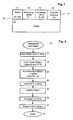
- Fig. 1 schematically show the data elements of a data structure, as used for the procedure according to the present invention in non-volatile data storage.
- the data structure 10 contains management data 11 and payload data 12.
- the management data 11 contains a status data element 13, an age rank counter 14, a predecessor index 15 and a virtual address 16.
- a memory segment can be referenced independently of its physical address.
- the predecessor index 15 contains a reference to the memory segment previously provided with the virtual address 16.
- the physical address of the old memory segment can be used as a reference.
- the necessary memory space for the data elements 15, 16 or their size in bits or bytes depends on the number of physical addresses of the memory segments used. This number can be limited by not providing all memory segments of a data memory for virtual addressing and / or atomic write operations.
- the age rank counter 14 is coded by three bits. Only one bit of the age rank counter 14 deviates from the deleted state of the data elements in the data memory. For the described embodiments, it is assumed that a flash memory page, the fast writing of allows a value of 1 to a value of 0 and requires a slower erase from the value 0 to the value 1.
- an age rank of the values is defined so that each value is considered to be older than a corresponding comparison value.
- the age ranking can be defined as follows: (1,1,0) is older than (1,0,1), (1,0,1) is older than (0,1,1) and (0,1, 1) is older than (1,1,0).
- the status data element 13 is coded by two bits S1 and S0.
- the following figures are used as values for a status in the following figures: (1,1) for an erased memory segment, (1,0) for a written memory segment whose atomic writing process has not yet been completed, and (0,0) for a memory segment after completed atomic write.
- FIG Fig. 3 A method for securely writing data to a memory segment at steps 20 through 28 is described with reference to FIG Fig. 2 described.
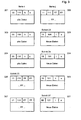
- the changes of values within the data structures of the two memory pages i and j involved by such a method sequence is shown in FIG Fig. 3 ,
- the memory page i contains a status data item with the value (0,0).
- the memory page i thus contains the currently valid data that can be addressed via the virtual address a.
- the data of the memory page j are cleared in the initial state 302, so that all the bits of the memory page have the value 1.
- the old data in memory page i should be replaced by new data.
- the counter C (n) of the memory page i is first read out in a step 21. From a ring buffer which will be described later, in a step 22, a page index j of the next memory page to be used is read out.
- the next-oldest value is determined according to the predetermined ranking.
- the value of the age increment counter C (n + 1) of the new memory page, which identifies this as the older of the two memory pages involved, is (1,0,1) in this case.
- the new data is written in the memory page j.
- the old data of the memory page i remain unchanged in state 303.
- the new data of memory page j in state 323 in the management data contains a status data item with the value (1,1) and the age rank counter with the value (1,0,1).
- the predecessor index in the management data in state 323 refers to the memory page i.
- the virtual address of the memory page j is set equal to the virtual address of the predecessor memory page i, ie it also has the value a.
- a step 24 of the method according to Fig. 2 the status bit S0 of the memory page j is set to zero. In addition to the still unchanged values of the memory page i in the state 304, this change can be seen in the status data element of the memory page j in the state 324.
- the memory page i is deleted. In state 325 of memory page i, all data is already cleared.
- the page index of the deleted memory page i is written in a ring 26 in the ring buffer.
- the FIFO stores the indexes of the available and deleted memory pages.
- the indexes of pages that are currently being deleted are pushed into the circular buffer and the indexes are taken from a memory page to be used for a write at the other end of the circular buffer.
- the use of the memory pages is thus distributed evenly to all memory pages of the data memory. Especially with flash data memories, which allow only a limited number of erase cycles, this can increase the overall life of the data memory.
- the status bit S1 of the memory page j is set to zero.
- the status of memory page j indicates in state 327 that the atomic transaction is complete and memory page j is to be used as the current memory page for virtual address a.
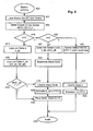
- FIG. 4 illustrates a method 400 to 450 for status checking or for returning data after a power interruption that occurs during an atomic transaction according to the method Fig. 2 occured.
- a procedure is usually performed upon a reboot of the smart card after a reset (forced reboot) or a power failure to ensure that the data used is in a consistent state.
- a first step 401 the administration data, in particular at least the status data, of all pages to be checked are read out.
- a number n of pages for which the status data item has the value (1,0) is counted in a step 402. According to the branches 410 and 420, the method is continued depending on the determined number n.
- n 1
- a reference k_old to the predecessor side is read from the corresponding memory page k in a step 411.
- the status data item of the old page is read out in step 412. If the status data item indicates, according to branch 413, that the old memory page has not yet been deleted, the old memory page with the index k_old is deleted in a step 424 and the index k_old is written into the ring buffer (step 425). Regardless of the branch 413, the status bit S1 of the page k is set to zero in a step 426.
- both age-rank counters Ci and Cj of memory pages i and j are read in a step 421.
- An age counter can prove to be the elder if it corresponds to a deleted state or if, according to the pre-defined definition, he is to be considered the elder.
- step 424 the older memory page is then deleted.
- the page index of the deleted memory page is written in the circular buffer in step 425.
- step 426 again sets the status page S1 of the new memory page to zero.
- a step 431 it is checked whether there exists a memory page n provided with a status (1,1) and other management data which is not erased. Such a page n is deleted in a step 432 and the page index n is written in a ring buffer in a step 433.
- steps 431 to 433 may alternatively be performed in the step of reading 401.
- steps 431 through 432 and 413 are optional steps of the method.
- the indices of the memory pages treated by these steps are no longer or not yet stored in the ring buffer and therefore are no longer used. Cleaning up the data memory by evaluating and handling these memory pages can therefore be done independently of the return of data to atomic transactions.
- the age rank counter allows uniquely identifying and deleting the older memory page (steps 420 through 426).
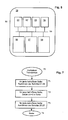
- a portable data carrier 50 The basic functional elements of a portable data carrier 50 are shown.
- a chip card, a USB token or a SIM card for a terminal of a mobile radio system can be present as a portable data carrier.
- an interface 52 is provided, which enables contactless and / or contact-based communication with external components or further components arranged in the mobile data carrier.
- a cryptographic unit 53 for performing cryptographic calculations as well as a detector or sensor 54 for detecting external attacks against the mobile data carrier are also present.
- memory elements are provided a volatile memory (RAM) 56, a non-rewritable memory (ROM) 57 and a non-volatile and segmented memory (flash EEPROM) 58.
- RAM volatile memory
- ROM non-rewritable memory
- flash EEPROM flash EEPROM
- the elements 51 to 54 and 56 to 58 are connected to each other at least via a line 55, preferably a bus.
- the mobile data carrier has its own power supply.
- the memory segments of the data memory 58 can, as in Fig. 6 shown, adapted according to the invention and / or, as in the Fig. 2 . 4 . 7 or 8th shown used.
- a control software for executing a corresponding method may be stored in one of the memory elements 56 to 58.
- FIG. 7 Fig. 3 illustrates the flow according to one embodiment of the present invention for a complex transaction.
- the complex transaction combines a plurality of steps in which data can be written into memory segments, respectively.
- the complex atomic transaction after Fig. 7 should along with the repatriation after Fig. 8 ensure that the memory segments affected by the complex transaction are either all changed or all are unchanged.
- a corresponding method 70 to 74 the sequence of steps 21 to 23 is first of all determined in a step 71 for each memory page concerned Fig. 2 executed.
- the reading of the counter of the page i, the reading of a new page index from the ring buffer, and the writing of the new pages to the page j are executed.
- the status bit S0 set to zero in a step 72 of the complex atomic transaction for each of the affected memory pages.
- a higher-level step 73 with the sub-steps 25 to 27 of Fig. 2 executed individually for each affected memory page.
- the step 73 includes clearing the old page, writing the old page index into the ring buffer, and setting the status bit S1 to zero in the new page.
- FIG. 8 The method 800 to 850 shown for a complex status check or for handling interruptions during a complex atomic transaction is according to the method Fig. 7 customized.
- the method begins with a loop 801, 823, 824 in which the status is read out for all memory pages n in a step 802.
- the next page of memory in the loop is continued if, as shown at branch 810, the status of the memory page is (1,1) and, according to branch 811, the administrative data is already cleared. If, on the other hand, the status of the memory page has the value (0, 1) or if the memory page management data are not deleted, a corresponding memory page is deleted in a step 821 according to branches 820 and 811 and the page index is written into the ring buffer in a step 822.
- the status of the memory page is (1,0)
- at least the index n of the memory page is stored in a list 831.
- the list thus comprises, for each memory page to be further processed, at least the index, which is preferably formed by the physical or the virtual address of the memory page. Further administrative data already read from the memory page, which are still used in the course of the procedure, in particular the predecessor reference (k_old) and the age rank counter, can likewise be stored in the list.
- a branch 840 checks for conflicts in the list of memory pages with the status (1,0). A conflict exists when two memory pages in the list specify each other as respective predecessor page. For such a conflict case, in a step 841, the older memory page is determined from the age rank counts C1 and C2 of the conflicting memory pages.
- the list entries are then processed individually.
- a pointer pointing to the list entry being edited is set to the first list entry (step 842).
- the older memory page k_alt is cleared and the page index k_alt is written into the circular buffer in a step 844.
- the status page S1 of the new memory page is set to zero in a step 845.
- Steps 843 through 845 are processed for all entries in the list by transitioning to the next list entry in step 846 and branch 847, checking for the end of the list.
- Steps 810, 811, and 820 through 822 are optional steps of the method.
- the indices of the memory pages treated by these steps are no longer or not yet stored in the ring buffer and therefore are no longer used. Cleaning up the data memory by evaluating and handling these memory pages can therefore be done independently of the return of data to atomic transactions.
- a table can be used to manage the virtual addresses of memory segments.
- Such a table can be kept in volatile or non-volatile memory and assigns the index of a memory page or its physical address to a used virtual address. All accesses to user data in the memory segments must then via the appropriate Table. When a mobile volume is powered on with a corresponding number of flash memory pages, that table is created in RAM by checking all flash memory pages.
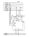
- Fig. 6 Control, address and data lines 611 through 618 connected to a flash memory page 601 are shown.
- the memory page 601 has, for example, 1x32-bit management data and 64x32-bit payload. It is merely indicated that, in addition to the memory page 601, further memory pages 602 are arranged in the corresponding data memory, which are respectively designed accordingly.
- the signal of a control line 615 indicates whether either the payload or the management data of the memory page should be accessed.
- the signal is set on the control line 611, the data addressed via the low address line signal 617 is output to the data line 618.
- the signal of the control line 612 is set, the value currently on the data line 618 is written in the memory page.
- the signal is set on a control line 613, the entire memory page 601 is deleted, ie both the user data and the management data are set to 0xFF.
- the signal of a control line 614 indicates whether the addressing of a memory page takes place via the physical addresses (direct) or via the virtual addresses (associative) of the memory pages.
- a set signal on the data line 614 ( ⁇ ass / dir) encodes direct addressing.
- the "1" on the data line 615 ( ⁇ data / admin) encodes access to the management data and the "0" accesses the payload of the memory page.
- the memory page 601 is deactivated when the activation signal is equal to "0".
- the signals of the control lines 611 to 613 then have no effect. If the activation signal for the memory page 601 is "1", then the control signals of the control lines 611 to 613 have the above-described effect.
- the means for activating the memory page 601 comprise a read-only memory 626 in which the physical address of the page memory 601 is stored.
- a multiplexer 625 selects either the physical address 626 or the virtual address a of the page memory 601 in accordance with the control signal 614. The selected address is compared in a comparator 624 with the address on an address line 616.
- the memory page 601 When the memory page 601 is referenced by the address line 616, it is determined by an AND gate 621, an OR gate 622 and a NOR gate 623 whether the memory page is for erasing, reading or writing according to one of the control signals 611 to 613 is enabled or activated.
- the memory page is enabled for access via the OR gate 622 when the control signal 614 indicates direct addressing via a physical address.
- the memory page is also enabled when a status S1, S0 with the value (0,0), which is evaluated via the NOR gate 623, is present.
- Activation means are provided at least for each memory page which is to be managed via a corresponding status and to be virtually addressable.
- an atomic write operation is performed by using a return buffer by saving the old data for one page with 64 * 32 bits payload (64 * 60 ⁇ s), clearing the page (8000 ⁇ s), writing the new data (64 * 60 ⁇ s) and erase the feedback buffer (8000 ⁇ s) for a total of 23680 ⁇ s.
- a data store may have a first group of memory pages dedicated to a secure write and a second group of memory pages that are not intended for atomic writes.
- a data memory for example, only the memory pages of the first group with activating means could after Fig. 6 be equipped.
- deletion of the memory pages is preferably carried out as described. For example, to reduce the processing time of a complex transaction, the steps of deleting a memory page may be skipped. The affected memory pages then have to be "erased" instead of being deleted. For this, the status data element is extended by a corresponding bit, which is written in the State signals this status. At a suitable later time, the memory pages to be deleted are then deleted.
Landscapes
- Techniques For Improving Reliability Of Storages (AREA)
- Read Only Memory (AREA)
- Information Retrieval, Db Structures And Fs Structures Therefor (AREA)
Claims (14)
- Procédé de protection de données dans une mémoire de données non volatile subdivisée en segments de mémoire d'un support de données portable, les données comprenant dans les segments de mémoire des données administratives pour les segments de mémoire respectifs, avec les étapes suivantes dans le support de données portable :écriture (23), dans un premier segment de mémoire de la mémoire de données, de nouvelles données qui doivent remplacer des anciennes données dans un deuxième segment de mémoire de la mémoire de données ;effacement (25) du deuxième segment de mémoire ;modification (24, 27) d'un élément de données de statut (13) dans les données administratives du premier ou du deuxième segment de mémoire afin de marquer les nouvelles données dans le premier segment de mémoire en tant que données mémorisées devant être utilisées,caractérisé en ce que
les données administratives des segments de mémoire contenant respectivement un renvoi (15) au prédécesseur, au segment de mémoire dans lequel des données furent précédemment adressées ;
les données administratives des segments de mémoire comportent respectivement des données de rang d'ancienneté (14) en tant qu'élément de données supplémentaire qui, dans le cas où l'étape de l'effacement (25) n'est pas complètement accomplie, rend possible la détermination du rang d'ancienneté des données se trouvant dans le deuxième segment de mémoire par rapport aux données se trouvant dans le premier segment de mémoire aussi dans le cas où les renvois aux prédécesseurs renvoient tous les deux réciproquement l'un à l'autre ; et
en ce que les données de rang d'ancienneté (14) peuvent coder au moins trois états et se distinguent en seulement un bit d'un état effacé. - Procédé selon la revendication 1, caractérisé en ce que l'étape de la modification (24, 27) de l'élément de données de statut (13) comprend :Première modification (24) de l'élément de données de statut (13) afin d'indiquer que le premier segment de mémoire a été complètement écrit etDeuxième modification (27) de l'élément de données de statut (13) afin d'indiquer que le deuxième segment de mémoire a été complètement effacé.
- Procédé selon une des revendications de 1 à 2, caractérisé en ce que, pour l'étape de l'écriture (23), les données de rang d'ancienneté (14) du premier segment de mémoire sont déterminées en fonction des données de rang d'ancienneté du deuxième segment de mémoire.
- Procédé selon une des revendications de 2 à 3, caractérisé en ce que, pour la protection d'une opération comprenant un grand nombre de données à remplacer, les étapes suivantes sont, avant de passer ensuite à la prochaine étape, respectivement accomplies pour toutes les données à remplacer:l'étape de l'écriture (23) des nouvelles données ;l'étape de la première modification (24) de l'élément de données de statut (13); et une étape comprenant l'effacement (25) des anciennes données et la deuxième modification (24) de l'élément de données de statut (13).
- Procédé de protection de données dans une mémoire de données non volatile subdivisée en segments de mémoire d'un support de données portable, les données comprenant dans les segments de mémoire des données administratives pour les segments de mémoire respectifs, avec les étapes dans le support de données portable :Lecture (401, 802) de données administratives d'un premier segment de mémoire qui contiennent un élément de données de statut et un renvoi à un segment de mémoire prédécesseur du premier segment de mémoire ;Dépouillement des données administratives lues, l'élément de données de statut contenu dans les données administratives lues du premier segment de mémoire étant utilisé (402, 810) ; etEffacement (424, 432, 821) d'un segment de mémoire en fonction du résultat de l'étape du dépouillement ;caractérisé en ce que,
lors de l'étape du dépouillement, des données de rang d'ancienneté sont utilisées en tant qu'élément de données supplémentaire des données administratives du premier segment de mémoire (422, 841) afin de déterminer le rang d'ancienneté des données du premier segment de mémoire par rapport à des données d'un deuxième segment de mémoire, de telle sorte que la détermination est possible aussi dans le cas où les renvois aux prédécesseurs renvoient tous les deux réciproquement l'un à l'autre ; et
en ce que lors de l'étape de l'effacement (424, 843), le premier ou le deuxième segment de mémoire est effacé en fonction du résultat de l'étape du dépouillement et
en ce que les données de rang d'ancienneté (14) peuvent coder au moins trois états et en ce que les données de rang d'ancienneté (14) se distinguent en seulement un bit d'un état effacé. - Procédé selon la revendication 5, caractérisé en ce que l'étape du dépouillement (402, 810) de l'élément de données de statut est effectuée pour les segments de mémoire de la mémoire de données afin d'effectuer l'étape du dépouillement (411, 422, 840) et l'effacement (824, 843) du premier ou du deuxième segment de mémoire en fonction d'un nombre des segments de mémoire ayant un élément de données de statut indiquant un effacement incomplet d'un ancien segment de mémoire.
- Procédé selon une des revendications de 5 à 6, caractérisé en ce que, dans le cas où deux éléments de données de statut indiquent un effacement incomplet, les données de rang d'ancienneté (14) sont utilisées pour la détermination de la page la plus ancienne.
- Procédé selon une des revendications de 5 à 7, caractérisé en ce que, dans le cas où seulement un élément de données de statut indique un effacement incomplet, le renvoi (15) est utilisé pour la détermination de la page la plus ancienne.
- Procédé selon une des revendications de 5 à 8, caractérisé par les étapes du procédé selon la revendication 1.
- Support de données portable comportant une structure de données pour l'administration de données dans une mémoire de données non volatile subdivisée en segments de mémoire, la structure de données contenant des données administratives (11) et des données utiles (12) dans les segments de mémoire (10), les données administratives (11) comprenant des données de statut (13) pour le marquage d'un état du segment de mémoire respectif, et les données administratives comprenant un renvoi au prédécesseur (14), caractérisé en ce que les données administratives comprennent en outre des données de rang d'ancienneté (15) qui, quand les données de statut (13) d'un premier segment de mémoire (i) indiquent un effacement non complet d'un deuxième segment de mémoire (j), rendent possible une détermination du rang d'ancienneté relatif des données se trouvant dans le deuxième segment de mémoire (j) par rapport aux données se trouvant dans le premier segment de mémoire (i), aussi dans le cas où les renvois aux prédécesseurs renvoient tous les deux réciproquement l'un à l'autre, et en ce que les données de rang d'ancienneté (14) peuvent coder au moins trois états et se distinguent en seulement un bit d'un état effacé.
- Support de données portable comprenant des moyens adaptés à la réalisation d'un procédé selon une des revendications de 1 à 9.
- Appareil de communication mobile comprenant un support de données portable selon la revendication 11.
- Système de communication mobile comprenant un appareil de communication mobile selon la revendication 12.
- Système de réalisation d'une transaction protégée, comprenant un grand nombre de supports de données portables selon la revendication 10 qui contiennent des données relatives à des personnes, et au moins une unité dotée de moyens de communication avec un des supports de données.
Applications Claiming Priority (2)
| Application Number | Priority Date | Filing Date | Title |
|---|---|---|---|
| DE102004005290A DE102004005290B3 (de) | 2004-02-03 | 2004-02-03 | Verfahren und Vorrichtung zur Absicherung von Daten in einem nichtflüchtigen Datenspeicher |
| DE102004005290 | 2004-02-03 |
Publications (3)
| Publication Number | Publication Date |
|---|---|
| EP1564754A2 EP1564754A2 (fr) | 2005-08-17 |
| EP1564754A3 EP1564754A3 (fr) | 2006-09-06 |
| EP1564754B1 true EP1564754B1 (fr) | 2009-07-29 |
Family
ID=34683970
Family Applications (1)
| Application Number | Title | Priority Date | Filing Date |
|---|---|---|---|
| EP04030429A Expired - Lifetime EP1564754B1 (fr) | 2004-02-03 | 2004-12-22 | Procédé et dispositif pour gérer des données dans une mémoire non-volatile |
Country Status (3)
| Country | Link |
|---|---|
| EP (1) | EP1564754B1 (fr) |
| AT (1) | ATE438179T1 (fr) |
| DE (2) | DE102004005290B3 (fr) |
Families Citing this family (3)
| Publication number | Priority date | Publication date | Assignee | Title |
|---|---|---|---|---|
| DE102008051575A1 (de) | 2008-10-14 | 2010-04-15 | Giesecke & Devrient Gmbh | Verfahren und Vorrichtung zur Verwaltung eines Datenspeichers |
| DE102011107435A1 (de) * | 2011-07-15 | 2013-01-17 | Giesecke & Devrient Gmbh | Verfahren zum Erkennen von gelöschten Speicherbereichen |
| CN108922278B (zh) * | 2018-08-20 | 2021-07-23 | 广东小天才科技有限公司 | 一种人机交互方法及学习设备 |
Family Cites Families (7)
| Publication number | Priority date | Publication date | Assignee | Title |
|---|---|---|---|---|
| US5437012A (en) * | 1993-04-19 | 1995-07-25 | Canon Information Systems, Inc. | System for updating directory information and data on write once media such as an optical memory card |
| FR2730833B1 (fr) * | 1995-02-16 | 1997-03-28 | Gemplus Card Int | Procede de mise a jour securisee de memoire eeprom |
| US6763424B2 (en) * | 2001-01-19 | 2004-07-13 | Sandisk Corporation | Partial block data programming and reading operations in a non-volatile memory |
| JP4654531B2 (ja) * | 2001-04-20 | 2011-03-23 | パナソニック電工株式会社 | ブロック消去型記憶媒体の管理装置 |
| JP3692313B2 (ja) * | 2001-06-28 | 2005-09-07 | 松下電器産業株式会社 | 不揮発性メモリの制御方法 |
| CN1255733C (zh) * | 2001-07-25 | 2006-05-10 | 索尼株式会社 | 非易失性存储器和非易失性存储器的数据改写方法 |
| JP2003157204A (ja) * | 2001-11-20 | 2003-05-30 | Canon Inc | データ書き換え装置及びデータ書き換え方法並びに記憶媒体 |
-
2004
- 2004-02-03 DE DE102004005290A patent/DE102004005290B3/de not_active Expired - Fee Related
- 2004-12-22 AT AT04030429T patent/ATE438179T1/de not_active IP Right Cessation
- 2004-12-22 EP EP04030429A patent/EP1564754B1/fr not_active Expired - Lifetime
- 2004-12-22 DE DE502004009819T patent/DE502004009819D1/de not_active Expired - Fee Related
Also Published As
| Publication number | Publication date |
|---|---|
| EP1564754A3 (fr) | 2006-09-06 |
| ATE438179T1 (de) | 2009-08-15 |
| EP1564754A2 (fr) | 2005-08-17 |
| DE102004005290B3 (de) | 2005-07-21 |
| DE502004009819D1 (de) | 2009-09-10 |
Similar Documents
| Publication | Publication Date | Title |
|---|---|---|
| DE60030876T2 (de) | Bereichsverwaltung eines nichtflüchtigen Speichers mit hoher Kapazität | |
| DE19882933B4 (de) | Flash-Speicher-Unterteilung für Lese-während-Schreiboperationen | |
| DE69316576T2 (de) | IC Karte mit alterunggeschützten Daten und Programmen | |
| DE69401291T2 (de) | Integrierte Schaltung für Speicherkarte und Verfahren zum Abzählen der Einheiten in einer Speicherkarte | |
| DE102009033961A1 (de) | Emulation eines einmal programmierbaren Speichers | |
| EP1183690B1 (fr) | Ensemble memoire avec hachage des adresses | |
| DE602004008240T2 (de) | Verfahren zum Verwalten von defekten Speicherblöcken in einem nicht-flüchtigen Speicher und nicht-flüchtiger Speicher zur Ausführung des Verfahrens | |
| DE10192507B4 (de) | Verfahren und Vorrichtung für die Vorhersage von Lösch- und Schreibzeiten von Flash-Speichern | |
| DE102007062674A1 (de) | Integrierte Schaltkreise, Speicher-Steuerungseinheit und Speichermodule | |
| DE60317801T2 (de) | Verfahren und vorrichtung zur erkennung von fehlern während des schreibens in einen nichtflüchtigen speicher | |
| EP3885957A1 (fr) | Dispositif de mémorisation de données dans une mémoire non volatile | |
| EP1564754B1 (fr) | Procédé et dispositif pour gérer des données dans une mémoire non-volatile | |
| DE4302754C1 (de) | Monolithisch integrierte Datenspeicheranordnung und Verfahren zu deren Betrieb | |
| DE10321104B4 (de) | Verfahren zur Ablage von veränderlichen Daten | |
| EP1559111B1 (fr) | Procede de fonctionnement d'un ensemble memoire | |
| DE10059006A1 (de) | Verfahren und System zur sicheren Verwaltung von Dateien in nichtflüchtigen Speichern | |
| DE112021005473T5 (de) | System mit anwachsendem geschütztem speicherbereich und löschschut | |
| EP1675008B1 (fr) | Traitement d'objets de données dans une mémoire réinscriptible non-volatile | |
| EP1505536B1 (fr) | Stockage d'élements de données dans une mémoire nonvolatile d'un support de données portable | |
| EP1517333B1 (fr) | Drapeau pour mémoire asymétrique avec drapeau indicant l'état concernant la proframmarion et l'éffacement | |
| DE102006013759B4 (de) | Verfahren und Recheneinheit zum Betreiben einer Speichereinrichtung | |
| DE19738712C2 (de) | Nichtflüchtiger Speicher mit zu Subblöcken zusammengefaßten Speicherzellen | |
| WO2002099650A2 (fr) | Procede destine a gerer la memoire d'une carte a puce | |
| DE102014112496A1 (de) | Speicherverwaltung für eine Chipkarte | |
| EP1968073B1 (fr) | Procédé destiné à l'écriture de données dans la mémoire d'un support de données portatif |
Legal Events
| Date | Code | Title | Description |
|---|---|---|---|
| PUAI | Public reference made under article 153(3) epc to a published international application that has entered the european phase |
Free format text: ORIGINAL CODE: 0009012 |
|
| AK | Designated contracting states |
Kind code of ref document: A2 Designated state(s): AT BE BG CH CY CZ DE DK EE ES FI FR GB GR HU IE IS IT LI LT LU MC NL PL PT RO SE SI SK TR |
|
| AX | Request for extension of the european patent |
Extension state: AL BA HR LV MK YU |
|
| PUAL | Search report despatched |
Free format text: ORIGINAL CODE: 0009013 |
|
| AK | Designated contracting states |
Kind code of ref document: A3 Designated state(s): AT BE BG CH CY CZ DE DK EE ES FI FR GB GR HU IE IS IT LI LT LU MC NL PL PT RO SE SI SK TR |
|
| AX | Request for extension of the european patent |
Extension state: AL BA HR LV MK YU |
|
| 17P | Request for examination filed |
Effective date: 20070306 |
|
| AKX | Designation fees paid |
Designated state(s): AT BE BG CH CY CZ DE DK EE ES FI FR GB GR HU IE IS IT LI LT LU MC NL PL PT RO SE SI SK TR |
|
| 17Q | First examination report despatched |
Effective date: 20070430 |
|
| GRAP | Despatch of communication of intention to grant a patent |
Free format text: ORIGINAL CODE: EPIDOSNIGR1 |
|
| GRAS | Grant fee paid |
Free format text: ORIGINAL CODE: EPIDOSNIGR3 |
|
| GRAA | (expected) grant |
Free format text: ORIGINAL CODE: 0009210 |
|
| AK | Designated contracting states |
Kind code of ref document: B1 Designated state(s): AT BE BG CH CY CZ DE DK EE ES FI FR GB GR HU IE IS IT LI LT LU MC NL PL PT RO SE SI SK TR |
|
| REG | Reference to a national code |
Ref country code: GB Ref legal event code: FG4D Free format text: NOT ENGLISH |
|
| REG | Reference to a national code |
Ref country code: CH Ref legal event code: EP |
|
| REG | Reference to a national code |
Ref country code: IE Ref legal event code: FG4D |
|
| REF | Corresponds to: |
Ref document number: 502004009819 Country of ref document: DE Date of ref document: 20090910 Kind code of ref document: P |
|
| NLV1 | Nl: lapsed or annulled due to failure to fulfill the requirements of art. 29p and 29m of the patents act | ||
| PG25 | Lapsed in a contracting state [announced via postgrant information from national office to epo] |
Ref country code: FI Free format text: LAPSE BECAUSE OF FAILURE TO SUBMIT A TRANSLATION OF THE DESCRIPTION OR TO PAY THE FEE WITHIN THE PRESCRIBED TIME-LIMIT Effective date: 20090729 Ref country code: IS Free format text: LAPSE BECAUSE OF FAILURE TO SUBMIT A TRANSLATION OF THE DESCRIPTION OR TO PAY THE FEE WITHIN THE PRESCRIBED TIME-LIMIT Effective date: 20091129 Ref country code: LT Free format text: LAPSE BECAUSE OF FAILURE TO SUBMIT A TRANSLATION OF THE DESCRIPTION OR TO PAY THE FEE WITHIN THE PRESCRIBED TIME-LIMIT Effective date: 20090729 Ref country code: ES Free format text: LAPSE BECAUSE OF FAILURE TO SUBMIT A TRANSLATION OF THE DESCRIPTION OR TO PAY THE FEE WITHIN THE PRESCRIBED TIME-LIMIT Effective date: 20091109 Ref country code: SE Free format text: LAPSE BECAUSE OF FAILURE TO SUBMIT A TRANSLATION OF THE DESCRIPTION OR TO PAY THE FEE WITHIN THE PRESCRIBED TIME-LIMIT Effective date: 20090729 |
|
| PG25 | Lapsed in a contracting state [announced via postgrant information from national office to epo] |
Ref country code: NL Free format text: LAPSE BECAUSE OF FAILURE TO SUBMIT A TRANSLATION OF THE DESCRIPTION OR TO PAY THE FEE WITHIN THE PRESCRIBED TIME-LIMIT Effective date: 20090729 Ref country code: SI Free format text: LAPSE BECAUSE OF FAILURE TO SUBMIT A TRANSLATION OF THE DESCRIPTION OR TO PAY THE FEE WITHIN THE PRESCRIBED TIME-LIMIT Effective date: 20090729 Ref country code: PL Free format text: LAPSE BECAUSE OF FAILURE TO SUBMIT A TRANSLATION OF THE DESCRIPTION OR TO PAY THE FEE WITHIN THE PRESCRIBED TIME-LIMIT Effective date: 20090729 |
|
| REG | Reference to a national code |
Ref country code: IE Ref legal event code: FD4D |
|
| PG25 | Lapsed in a contracting state [announced via postgrant information from national office to epo] |
Ref country code: PT Free format text: LAPSE BECAUSE OF FAILURE TO SUBMIT A TRANSLATION OF THE DESCRIPTION OR TO PAY THE FEE WITHIN THE PRESCRIBED TIME-LIMIT Effective date: 20091129 Ref country code: BG Free format text: LAPSE BECAUSE OF FAILURE TO SUBMIT A TRANSLATION OF THE DESCRIPTION OR TO PAY THE FEE WITHIN THE PRESCRIBED TIME-LIMIT Effective date: 20091029 |
|
| PG25 | Lapsed in a contracting state [announced via postgrant information from national office to epo] |
Ref country code: IE Free format text: LAPSE BECAUSE OF FAILURE TO SUBMIT A TRANSLATION OF THE DESCRIPTION OR TO PAY THE FEE WITHIN THE PRESCRIBED TIME-LIMIT Effective date: 20090729 Ref country code: RO Free format text: LAPSE BECAUSE OF FAILURE TO SUBMIT A TRANSLATION OF THE DESCRIPTION OR TO PAY THE FEE WITHIN THE PRESCRIBED TIME-LIMIT Effective date: 20090729 Ref country code: DK Free format text: LAPSE BECAUSE OF FAILURE TO SUBMIT A TRANSLATION OF THE DESCRIPTION OR TO PAY THE FEE WITHIN THE PRESCRIBED TIME-LIMIT Effective date: 20090729 Ref country code: CZ Free format text: LAPSE BECAUSE OF FAILURE TO SUBMIT A TRANSLATION OF THE DESCRIPTION OR TO PAY THE FEE WITHIN THE PRESCRIBED TIME-LIMIT Effective date: 20090729 Ref country code: EE Free format text: LAPSE BECAUSE OF FAILURE TO SUBMIT A TRANSLATION OF THE DESCRIPTION OR TO PAY THE FEE WITHIN THE PRESCRIBED TIME-LIMIT Effective date: 20090729 |
|
| PG25 | Lapsed in a contracting state [announced via postgrant information from national office to epo] |
Ref country code: SK Free format text: LAPSE BECAUSE OF FAILURE TO SUBMIT A TRANSLATION OF THE DESCRIPTION OR TO PAY THE FEE WITHIN THE PRESCRIBED TIME-LIMIT Effective date: 20090729 |
|
| PLBE | No opposition filed within time limit |
Free format text: ORIGINAL CODE: 0009261 |
|
| STAA | Information on the status of an ep patent application or granted ep patent |
Free format text: STATUS: NO OPPOSITION FILED WITHIN TIME LIMIT |
|
| BERE | Be: lapsed |
Owner name: GIESECKE & DEVRIENT G.M.B.H. Effective date: 20091231 |
|
| 26N | No opposition filed |
Effective date: 20100503 |
|
| PG25 | Lapsed in a contracting state [announced via postgrant information from national office to epo] |
Ref country code: MC Free format text: LAPSE BECAUSE OF NON-PAYMENT OF DUE FEES Effective date: 20100701 |
|
| REG | Reference to a national code |
Ref country code: CH Ref legal event code: PL |
|
| GBPC | Gb: european patent ceased through non-payment of renewal fee |
Effective date: 20091222 |
|
| PG25 | Lapsed in a contracting state [announced via postgrant information from national office to epo] |
Ref country code: BE Free format text: LAPSE BECAUSE OF NON-PAYMENT OF DUE FEES Effective date: 20091231 Ref country code: CH Free format text: LAPSE BECAUSE OF NON-PAYMENT OF DUE FEES Effective date: 20091231 Ref country code: GR Free format text: LAPSE BECAUSE OF FAILURE TO SUBMIT A TRANSLATION OF THE DESCRIPTION OR TO PAY THE FEE WITHIN THE PRESCRIBED TIME-LIMIT Effective date: 20091030 Ref country code: LI Free format text: LAPSE BECAUSE OF NON-PAYMENT OF DUE FEES Effective date: 20091231 |
|
| PG25 | Lapsed in a contracting state [announced via postgrant information from national office to epo] |
Ref country code: DE Free format text: LAPSE BECAUSE OF NON-PAYMENT OF DUE FEES Effective date: 20100701 |
|
| PG25 | Lapsed in a contracting state [announced via postgrant information from national office to epo] |
Ref country code: GB Free format text: LAPSE BECAUSE OF NON-PAYMENT OF DUE FEES Effective date: 20091222 |
|
| PG25 | Lapsed in a contracting state [announced via postgrant information from national office to epo] |
Ref country code: IT Free format text: LAPSE BECAUSE OF FAILURE TO SUBMIT A TRANSLATION OF THE DESCRIPTION OR TO PAY THE FEE WITHIN THE PRESCRIBED TIME-LIMIT Effective date: 20090729 |
|
| PG25 | Lapsed in a contracting state [announced via postgrant information from national office to epo] |
Ref country code: LU Free format text: LAPSE BECAUSE OF NON-PAYMENT OF DUE FEES Effective date: 20091222 |
|
| PG25 | Lapsed in a contracting state [announced via postgrant information from national office to epo] |
Ref country code: AT Free format text: LAPSE BECAUSE OF NON-PAYMENT OF DUE FEES Effective date: 20091222 |
|
| PG25 | Lapsed in a contracting state [announced via postgrant information from national office to epo] |
Ref country code: HU Free format text: LAPSE BECAUSE OF FAILURE TO SUBMIT A TRANSLATION OF THE DESCRIPTION OR TO PAY THE FEE WITHIN THE PRESCRIBED TIME-LIMIT Effective date: 20100130 |
|
| PG25 | Lapsed in a contracting state [announced via postgrant information from national office to epo] |
Ref country code: TR Free format text: LAPSE BECAUSE OF FAILURE TO SUBMIT A TRANSLATION OF THE DESCRIPTION OR TO PAY THE FEE WITHIN THE PRESCRIBED TIME-LIMIT Effective date: 20090729 |
|
| PG25 | Lapsed in a contracting state [announced via postgrant information from national office to epo] |
Ref country code: CY Free format text: LAPSE BECAUSE OF FAILURE TO SUBMIT A TRANSLATION OF THE DESCRIPTION OR TO PAY THE FEE WITHIN THE PRESCRIBED TIME-LIMIT Effective date: 20090729 |
|
| PGFP | Annual fee paid to national office [announced via postgrant information from national office to epo] |
Ref country code: FR Payment date: 20141212 Year of fee payment: 11 |
|
| REG | Reference to a national code |
Ref country code: FR Ref legal event code: ST Effective date: 20160831 |
|
| PG25 | Lapsed in a contracting state [announced via postgrant information from national office to epo] |
Ref country code: FR Free format text: LAPSE BECAUSE OF NON-PAYMENT OF DUE FEES Effective date: 20151231 |