EP1566830B1 - Procede servant a fabriquer une tranche de silicium sur isolant - Google Patents
Procede servant a fabriquer une tranche de silicium sur isolant Download PDFInfo
- Publication number
- EP1566830B1 EP1566830B1 EP20030774018 EP03774018A EP1566830B1 EP 1566830 B1 EP1566830 B1 EP 1566830B1 EP 20030774018 EP20030774018 EP 20030774018 EP 03774018 A EP03774018 A EP 03774018A EP 1566830 B1 EP1566830 B1 EP 1566830B1
- Authority
- EP
- European Patent Office
- Prior art keywords
- wafer
- soi
- wafers
- configuration
- layer
- Prior art date
- Legal status (The legal status is an assumption and is not a legal conclusion. Google has not performed a legal analysis and makes no representation as to the accuracy of the status listed.)
- Expired - Lifetime
Links
Images





Classifications
-
- H—ELECTRICITY
- H10—SEMICONDUCTOR DEVICES; ELECTRIC SOLID-STATE DEVICES NOT OTHERWISE PROVIDED FOR
- H10P—GENERIC PROCESSES OR APPARATUS FOR THE MANUFACTURE OR TREATMENT OF DEVICES COVERED BY CLASS H10
- H10P90/00—Preparation of wafers not covered by a single main group of this subclass, e.g. wafer reinforcement
- H10P90/12—Preparing bulk and homogeneous wafers
-
- H—ELECTRICITY
- H10—SEMICONDUCTOR DEVICES; ELECTRIC SOLID-STATE DEVICES NOT OTHERWISE PROVIDED FOR
- H10P—GENERIC PROCESSES OR APPARATUS FOR THE MANUFACTURE OR TREATMENT OF DEVICES COVERED BY CLASS H10
- H10P90/00—Preparation of wafers not covered by a single main group of this subclass, e.g. wafer reinforcement
- H10P90/19—Preparing inhomogeneous wafers
- H10P90/1904—Preparing vertically inhomogeneous wafers
- H10P90/1906—Preparing SOI wafers
- H10P90/1914—Preparing SOI wafers using bonding
- H10P90/1916—Preparing SOI wafers using bonding with separation or delamination along an ion implanted layer, e.g. Smart-cut
-
- H—ELECTRICITY
- H10—SEMICONDUCTOR DEVICES; ELECTRIC SOLID-STATE DEVICES NOT OTHERWISE PROVIDED FOR
- H10W—GENERIC PACKAGES, INTERCONNECTIONS, CONNECTORS OR OTHER CONSTRUCTIONAL DETAILS OF DEVICES COVERED BY CLASS H10
- H10W10/00—Isolation regions in semiconductor bodies between components of integrated devices
- H10W10/10—Isolation regions comprising dielectric materials
- H10W10/181—Semiconductor-on-insulator [SOI] isolation regions, e.g. buried oxide regions of SOI wafers
Definitions
- the present invention relates to a method for manufacturing a wafer and, more particularly, to a method for manufacturing an SOI (Silicon on Insulator) wafer constituted of an SOI layer, an insulating layer, and a support substrate which is obtained by an ion implantation delamination method or the like.
- SOI Silicon on Insulator
- an integration level in an integrated circuit has greatly increased, which has been accompanied by stricter required conditions imposed on a processing precision such as flatness or smoothness of a mirror-polished wafer surface.
- a processing precision such as flatness or smoothness of a mirror-polished wafer surface.
- an SOI wafer which is an ideal dielectric isolation substrate, has been used in applications to high frequency and high-speed devices mainly related to mobile communication equipment and medical equipment and further great increase in demand therefor is expected in the future.
- An SOI wafer 50 has a structure in which an SOI layer 52 (also referred to as a semiconductor layer or an active layer) for forming an element such as a single crystal silicon layer is formed on an insulating layer 54 (also referred to as a buried oxide (BOX) film layer or simply an oxide film layer) such as a silicon oxide film.
- the insulating layer 54 is formed on a support substrate 56 (also referred to as a substrate layer) and the SOI wafer 50 has a structure in which the insulating layer 54 and the SOI layer 52 are sequentially formed on the support substrate 56.
- reference numeral 60 designates an unbonded region
- reference numeral 62 designates a terrace, which will be described later.
- an SOI wafer 50 having the SOI structure in which the SOI layer 52 and the support substrate 56 are made of, for example, silicon and the insulating layer 54 is made of, for example, a silicon oxide film there are exemplified an SIMOX (Separation by implanted oxygen) method in which oxygen ions are implanted into a silicon single crystal at a high concentration and thereafter the single crystal is subjected to heat treatment at a high temperature to form an oxide film thereon; and a bonding method (an adhering method) in which two mirror-polished wafers are bonded with each other without the use of an adhesive, followed by processing one of the bonded wafers into a thin film.
- SIMOX Separatation by implanted oxygen
- the SIMOX method can controllably determine a film thickness of an active layer portion (an SOI layer) 52 to serve as a device active region by an acceleration voltage in oxygen ion implantation, there is an advantage that a thin active layer high in film thickness uniformity can be easily obtained, whereas there have remained many issues of reliability of a buried oxide (BOX) film (an insulating layer) 54, crystallinity in an active layer, and others.
- an active layer portion an SOI layer
- BOX buried oxide
- a wafer bonding method is carried out in such a way that an oxide film (an insulating layer) 54 is formed on at least one of two single crystal silicon mirror-polished wafers, then both wafers are adhered with each other without using an adhesive, then the adhered wafers are subjected to heat treatment (usually at a temperature in the range of 1100°C to 1200°C) to strengthen bonding therebetween and thereafter one of the wafers is thinned into a thin film by grinding or wet etching, followed by mirror-polishing the surface of the thin film so as to obtain an SOI layer 52; which leads to advantages that reliability of the buried oxide (BOX) film (an insulating layer) 54 is high and crystallinity of the SOI layer is also good.
- the thus adhered SOI wafer 50 is subjected to mechanical processing such as grinding or polishing into a thin film, and hence the obtained SOI layer 52 have limitations in its film thickness and uniformity.
- an SOI wafer 50 As a method for manufacturing an SOI wafer 50, it has very recently started to pay attention to a method for manufacturing an SOI wafer by bonding and delaminating an ion implanted wafer.
- This method is also referred to as an ion implantation delamination method, which is such a technique that two silicon wafers are provided to be ready for use; an oxide film (an insulating layer) is formed on at least one silicon wafer; hydrogen ions or rare gas ions are implanted onto an upper surface of the one silicon wafer; a micro-bubble layer (an enclosed layer) is formed in the interior of the one wafer, the surface onto which the ions are implanted is contacted and adhered with the other silicon wafer through the oxide film interposed therebetween; thereafter by applying heat treatment to the adhered wafers, a part of the one wafer is delaminated with the micro-bubble layer as a cleavage plane for the rest of the one wafer to become a thin film; and heat treatment
- FIG. 14 further detailed description will be given of the ion implantation delamination method showing one example of a set of main steps thereof.
- a base wafer 56a serving as a support substrate 56 and a bond wafer 52a from which an SOI layer 52 is formed [ FIG. 14(a) , step 100].
- these wafers for example, mirror-polished silicon single crystal wafers are used.
- An oxide film 54a serving as a buried oxide (BOX) film (an insulating layer) at a later step is formed on a surface of the bond wafer 52a [ FIG. 14(b) , step 102].
- This step is carried out as follows.
- thermal oxidation is applied on the bond wafer 52a of a silicon single crystal wafer to form a silicon oxide film on the bond wafer 52a.
- the formation of the oxide film may be performed on the surface of the base wafer 56a, not on the surface of the bond wafer 52a.
- the exemplary case where the oxide film 54a is formed on the bond wafer 52a side will be explained.
- H 2 SO 4 -H 2 O 2 mixed solution has been known in a field of wet cleaning with an abbreviation of SPM (Sulfuric Acid-Hydrogen Peroxide Mixture) and is a cleaning solution for removal of organic contaminants.
- SPM sulfuric Acid-Hydrogen Peroxide Mixture
- the bond wafer 52a in which the micro-bubble layer (the enclosed layer) 58 is formed is brought into close contact with the base wafer 56a at room temperature through the oxide film 54a on the surface of the bond wafer 52a onto which the ion implantation has been performed [ FIG. 14(d) , step 106].
- the SOI wafer 50 manufactured using the adhering method has, at this stage, a sectional structure in which the insulating film (layer) 54 and the SOI layer 52 are separately and sequentially laminated on one main surface of the support substrate 56.
- the insulating layer 54 and the SOI layer 52 are generally smaller in diameter than the support substrate 56 by a value of the order of several mm, usually about 3mm (hereinafter, this portion may be referred to as an unbonded region).
- step 112 a surface of the SOI layer 52 of the wafer having the SOI structure is modified and the thickness of the SOI layer 52 is controlled.
- the damage layer is removed by applying polishing with a small polishing stock removal usually called touch polishing.
- an SOI wafer 50 having a damage free thin film SOI layer 52 may be manufactured.
- organic matter or particles generated in the steps of manufacturing an SOI wafer may adversely affect the adhering interface to cause a decrease in yield.
- the influence of defects or the like present in the base wafer or the bond wafer is conceivable the influence of defects or the like present in the base wafer or the bond wafer.
- the problem of the organic matter or the particles can be solved to some extent by performing RCA cleaning or organic matter removing cleaning before wafers are adhered to each other.
- the RCA cleaning is a typical cleaning method in semiconductor processes using two cleaning liquids of two types, i.e., SC-1 (a liquid mixture of NH 4 OH/H 2 O 2 /H 2 O) and SC-2 (a liquid mixture of HCl/H 2 O 2 /H 2 O) as bases.
- SC-1 a liquid mixture of NH 4 OH/H 2 O 2 /H 2 O
- SC-2 a liquid mixture of HCl/H 2 O 2 /H 2 O
- SPM cleaning Organic matter removing cleaning called SPM cleaning may be employed.
- COP defect due to crystals
- a defect due to processing, and the like become issues. These defects can be reduced to some extent by controlling manufacturing conditions. When using a wafer having fewer defects, generation of voids can also be reduced.
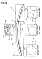
- FIG. 15 is a schematic view showing results of observation by a laser microscope with a confocal optical system on a part of the outer peripheral portion of the SOI wafer 50.
- a terrace 62 the boundary between the unbonded region 60 (a portion where the support substrate 56 can be seen when the wafer is observed from the SOI layer 52 side) and the SOI layer 52.
- a circular void 70 is observed at a portion away from the terrace 62 by a predetermined distance.
- the void 70 was generated at a position away from the wafer outer periphery by about 5 mm (145 mm from the center when a wafer having a diameter of 300 mm is used) with reference to the outer peripheral portion of the base wafer.
- the part (b) shows the void 70 generated at a position away from the center by 145.1 mm
- the part (c) shows the void 70 generated at a position away from the center by 145.4 mm
- the part (d) shows the void 70 generated at a position away from the center by 144.9 mm.
- EP1189266A1 shows a prior art manufacturing method for an SOI wafer by bonding two wafers using starting wafers with high flatness and a reduced polishing sag to reduce the unbonded region.
- the present invention has been made in consideration of the above problems, and a main object thereof is to provide a method for manufacturing an SOI wafer that suppresses a void from being generated in an SOI wafer, especially, in an outer peripheral portion thereof to improve productivity.
- the present inventor has earnestly investigated a cause of frequent generation of voids at a specific position of the outer peripheral portion of an SOI wafer. As a result, it has become clear that a configuration of a starting wafer and processing such as cleaning influence the generation of voids. In particular, it has been revealed that control of the configuration of the outer peripheral portion of the wafer can considerably reduce the generation of voids.
- a first aspect of the method for manufacturing an SOI wafer according to the present invention comprises the steps of: forming an insulating layer on at least one wafer (a bond wafer) of two starting wafers; and adhering the one wafer to the other wafer (a base wafer) without an adhesive, wherein there is used as the starting wafer a wafer having an outer peripheral configuration with a configuration change width being 0.1 ⁇ m or less in a region of between 10 mm and 3 mm away from the outer periphery.
- the number of voids generated at a specific position in the wafer outer peripheral portion (the position away from a wafer outer periphery by about 5 mm) can be reduced.
- the configuration of the wafer outer periphery has also been studied.
- a wafer having small droop (sags) of the outer peripheral configuration is desirably used to reduce the unbonded region. It is surmised to some extent that a wafer flat to the outer periphery is preferred. However, it is difficult to actually manufacture such a flat wafer. Therefore, the peripheral sags have been improved, for example, by devising a chamfered configuration to reduce the unbonded region.
- a second aspect of the method for manufacturing an SOI wafer according to the present invention comprises the steps of: forming an insulating layer on at least one wafer (a bond wafer) of two starting wafers; and adhering the one wafer to the other wafer (a base wafer) without an adhesive, wherein there is used as the starting wafer a wafer having an outer peripheral configuration with a configuration change width being 0.1 ⁇ m or less in a region of between 10 mm and 3 mm away from the outer periphery and a slope being 0.002% or less at a position of 5 mm away from the outer periphery.
- the method for manufacturing an SOI wafer in which the insulating layer is formed on at least one wafer (a bond wafer) of the two starting wafers, and the wafer is adhered to the other wafer (a base wafer) without an adhesive agent there can be used the method comprising the steps of: forming an insulating layer on at least one wafer (a bond wafer) of two starting wafers; implanting hydrogen ions or rare gas ions through an upper surface of the one wafer (the bond wafer) to form a micro-bubble layer in the interior of the one wafer; thereafter bringing the surface of the one wafer through which the ions have been implanted into close contact with the other wafer (a base wafer) through the insulating layer interposed therebetween; then delaminating a part of the one wafer with the micro-bubble layer as a cleavage plane by applying heat treatment for the rest thereof to become a thin film; and bonding strongly the one wafer in the form of a thin film to the other wafer through the method compris
- voids are generated in the wafer outer peripheral portion in the delaminating step of an ion implantation delamination method or the like.
- the configuration of the starting wafer is very important to prevent the generation of the voids in the delaminating step.
- a third aspect of the method for manufacturing an SOI wafer according to the present invention comprises: a wafer processing step having a polishing step for mirror-polishing at least one main surface of at least one of two starting wafers; and an SOI wafer manufacturing step for adhering the two wafers including at least one mirror-polished wafer to each other to manufacture a wafer having an SOI structure, wherein in the wafer processing step, each of the starting wafers is processed such that an outer peripheral configuration of the wafer has a configuration change width of 0.1 ⁇ m or less in a region of between 10 mm and 3 mm away from the outer periphery.
- a fourth aspect of the method for manufacturing an SOI wafer according to the present invention comprises: a wafer processing having a polishing step for mirror-polishing at least one main surface of at least one of two starting wafers; and an SOI wafer manufacturing step for adhering the two wafers including at least one mirror-polished wafer to each other to manufacture a wafer having an SOI structure, wherein in the wafer processing step, each of the starting wafers is processed such that an outer peripheral configuration of the wafer has a configuration change width of 0.1 ⁇ m or less in a region of between 10 mm and 3 mm away from the outer periphery and a slope of 0.002% or less at a position of 5 mm away from the outer periphery.
- the wafer configuration is determined in the wafer processing step and the wafer having the configuration described above is processed by contriving, for example, a structure of a polishing head in the polishing step.
- a fifth aspect of the method for manufacturing an SOI wafer according to the present invention comprises: a wafer processing step having a polishing step for mirror-polishing at least one main surface of at least one of two starting wafers; and an SOI wafer manufacturing step for adhering the two wafers including at least one mirror-polished wafer to each other to manufacture a wafer having an SOI structure, wherein the configuration of the wafer obtained in the wafer processing step is evaluated, wafers each having an outer peripheral configuration with a configuration change width of 0.1 ⁇ m or less in a region of between 10 mm and 3 mm away from the outer periphery are sorted, and an SOI wafer is manufactured using the sorted wafers.
- a sixth aspect of a method for manufacturing an SOI wafer according to the present invention comprises: a wafer processing step having a polishing step for mirror-polishing at least one main surface of at least one of two starting wafers; and an SOI wafer manufacturing step for adhering the two wafers including at least one mirror-polished wafer to each other to manufacture a wafer having an SOI structure, wherein the configuration of the wafer obtained in the wafer processing step is evaluated, wafers each having an outer peripheral configuration with a configuration change width of 0.1 ⁇ m or less in a region of between 10 mm and 3 mm away from the outer periphery and a slope of 0.002% or less at a position of 5 mm away from the outer periphery are sorted, and an SOI wafer is manufactured using the sorted wafers.
- a wafer having the above characteristics can be perfectly manufactured in the above wafer processing step.
- the wafer processing step includes various steps, the same configurations are not always obtained therein.
- a wafer configuration is evaluated to sort and use a preferred wafer, so that generation of the voids can be reduced.
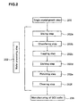
- FIG. 1 is a schematic flow chart showing an example of an order of steps in a method for manufacturing an SOI wafer according to the present invention.
- FIG. 14 shows an example of a method for manufacturing an SOI wafer, wherein an SOI structure is formed by a conventional adhering method (an ion implantation delamination method) as described above.
- adhering is performed such that the outer peripheral configurations of wafers to be used as starting materials of a bond wafer and a base wafer especially used in adhering are controlled.
- the mirror-polished wafer as shown in FIG. 1 , is generally manufactured through a single crystal growth step (step 200) of producing a single crystal ingot using a Czochralski (CZ) method or the like and a wafer processing step (step 202) of slicing the single crystal ingot to form a wafer and processing at least one main surface of the wafer to form a mirror-polished wafer.
- a wafer processing step step 202
- mirror polishing is performed such that a configuration change in a region ranging from 3 mm to 7 mm of the outer peripheral portion of the wafer is 0.1 mm or less.
- the wafer processing step (step 202) includes: a slicing step (step 202a) of slicing a single crystal ingot to obtain a thin disk-like wafer; a chamfering step (step 202b) of chamfering a peripheral edge portion of the wafer obtained through the slicing step to prevent cracking or chipping of the wafer; a lapping step (step 202c) of flattening the chamfered wafer; an etching step (step 202d) of removing processing deformation remaining on the surface of the chamfered and lapped wafer; a polishing step (step 202e) of mirror-polishing the surface of the wafer; and a cleaning step (step 202f) of cleaning the polished wafer to remove a polishing agent or dust particles deposited thereon.
- step 202 shows basic steps thereof, and sometimes other steps such as a heat treatment step and a surface grinding step may be added, or the same step may be divided into multiple sub-steps, or the step sequence may be changed. These steps are devised to manufacture a wafer having a high flatness level.
- the configuration of the wafer manufactured in the wafer processing step in particular, the configuration of the wafer outer peripheral portion is further exactly controlled; if necessary the wafer configuration is evaluated to sort only a suitable wafer (step 204); and an SOI wafer is manufactured using the sorted wafer as a starting wafer for the SOI wafer (step 206).
- a base wafer 56a serving as a support substrate 56 and a bond wafer 52a are prepared ( FIG. 14(a) ). Both the wafers are mirror-polished silicon single crystal wafers. As to the configuration of each of the wafers, there is used a wafer being free from a place where a configuration sharply changes in the wafer outer peripheral portion.
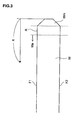
- the wafer outer peripheral portion is generally chamfered to prevent a wafer W from being cracked, and a chamfered portion Wm is formed.
- the wafer configuration of the chamfered portion Wm is to be neglected in evaluation, and is not an object to be measured.
- the width of the chamfered portion Wm is about 500 ⁇ m (0.5 mm).
- Actual configuration evaluation is frequently performed for a region except a region extending from the chamfered portion Wm toward the main surface side by about 3 mm or 2 mm, and further by about 1 mm, i.e., a measurement exclusion region R.
- a measurement exclusion region R is the measurement exclusion region
- reference symbol F1 designates a wafer main surface (a front surface); reference symbol F2, a wafer main surface (a rear surface); reference symbol R, a measurement exclusion region; reference symbol We, a wafer effective region; reference symbol X, a distance of X mm when an outer peripheral portion is X mm.
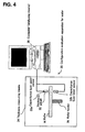
- the wafer configuration evaluating apparatus is not limited to a specific apparatus. However, for example, an apparatus shown in FIG. 4 can be used for the purpose. As the apparatus, there is preferably used an apparatus which scans a wafer surface at predetermined intervals and sequentially stores the measured configurations.
- the predetermined measurement interval on the wafer surface is preferably within 1 mm. Although the interval exceeds 0 mm as a matter of course, evaluation at finest possible intervals makes it possible to quantify a more correct configuration. At the present, the measurement is performed at intervals of about 0.05 mm.
- the configuration evaluation apparatus 30 measures displacements on the wafer surface in a direction perpendicular to the front surface and the rear surface of the wafer W placed on a wafer holder in the wafer plane to show the measurement results as displacement data or thickness data.
- reference numeral 28 designates a computer (an analyzing means); reference numeral 32, a thickness gauge; reference numeral 32a, a capacitance type upper sensor; reference numeral 32b, a capacitance type lower sensor; reference numeral 34, a thickness measuring means; and reference numeral 36, a wafer holder.
- a prescribed region on the wafer center side (extending from about 7 mm away from the wafer outer periphery to the wafer center side) was virtually flat, a part of this region was set as a reference zone (a reference value), and a change from the reference zone was checked.
- a reference zone a reference zone
- a reference zone is set such that a region of between 7 mm and 10 mm away from the wafer outer periphery is constant, and a rate of a configuration change in the region of between 7 mm and 10 mm away from the outer periphery is controlled.
- a wafer having a configuration the change of which is 0.1 ⁇ m or less in the above region is preferably used.
- the configuration of the starting wafer there is important a configuration in a bonded region after an SOI wafer is formed, and a region extending from the outer periphery by about 3 mm is an unbonded region. For this reason, measurement is preferably performed in the region extending from 3 mm away from the outer periphery toward the main surface side. In particular, when a judgment is made in a region of between about 3 mm and 10 mm away from the outer periphery, it can be inferred whether voids are easily generated or not. Even when the region is changed to some extent, inference can be made.
- the region is narrowed, there decreases the width of a configuration change of the existing wafer having a high flatness level, and hence it is difficult to discriminate the configuration change from a measurement error or the like, thereby the measurement accuracy being deteriorated.
- a large undulation component is picked up, and erroneous judgment may be performed.
- a portion in the vicinity of the outer periphery of the wafer for example a region extending from about 2 mm away from the outer periphery toward the main surface side can also be set.
- the configuration sharply changes in this region, and the configuration change influences the unbonded region more than generation of voids. For this reason, it is preferable for the present invention to include the above region.
- a wafer in which a configuration change within a prescribed range is controlled to be a prescribed value or less is used as a starting wafer of an SOI wafer.
- the wafer outer peripheral portion mainly sags (the outer peripheral portion is thin).
- the outer peripheral portion may rise (the outer peripheral portion is thick). The above configuration change value is obtained as an absolute value.
- a configuration profile is once differentiated, and the configuration change may be determined depending on the size of the slope (inclination) thereof.
- Configuration data of the wafer are measured at prescribed intervals on the wafer surface, the measured wafer configuration data are differentiated, and the obtained profile (the differentiated wafer configuration data) is analyzed.
- the wafer configuration measured as described above is not directly used, and the differentiated wafer configuration is analyzed, so that the configuration of the wafer outer peripheral portion can be accurately evaluated. In particular, a point of the local configuration change and the size of the inclination can be accurately evaluated.
- a value obtained by dividing a difference between No. (i+1) of the thickness data (yi+1) and No. (i) of the thickness data (yi) immediately before the data (yi+1) by the prescribed measurement interval (xi+1-xi) is calculated as a differential value (dyi), and the data is plotted on the middle point of (xi+1-xi).
- the configuration profile in FIG. 6 is differentiated and then changed into a differential profile as shown in FIGs. 7 and 8 .
- a configuration sharply changes in a wafer in which voids are easily generated (and at a portion where voids are easily generated).
- a solid line indicates a wafer in which voids are easily generated
- a dotted line indicates a wafer in which voids are less generated.
- an inclination is about 0.004% at a position of 5 mm away from the wafer outer periphery. This position is not limited to a specific position.
- voids are easily generated in the outer peripheral portion of a wafer using, as a starting wafer, a wafer in which a configuration change at the above level occurs in a region ranging from 4 mm away from the outer periphery toward the inside.
- a wafer in which a configuration change is controlled as described above is used to manufacture an SOI wafer.
- Wafers may be manufactured in advance in the wafer processing step so as to have the above configuration, or wafers may be sorted through evaluation.
- a polishing head is devised, or the hardness of a polishing cloth, a polishing pressure, and the like are controlled, so that a wafer having the configuration can be manufactured.
- An SOI wafer is manufactured using the wafers thus prepared. Manufacturing conditions or the like of an SOI wafer are not limited to specific conditions. As an example, a method for manufacturing an SOI wafer using an ion-implantation delamination method will be described below together with the flow chart in FIG. 14 .
- an oxide film 54a that will become a buried oxide film 54 (an insulating layer) at a later stage is formed on the surface (the entire surface) of a bond wafer 52a ( FIG. 14(b) , step 102).
- the oxide film 54a a silicon oxide film is formed by thermal oxidation.
- an oxide film may not be formed on the bond wafer 52a (a wafer into which ions are implanted), and an oxide film may be formed on a base wafer 56a.
- RCA cleaning or SPM cleaning to remove organic matter is performed (step 105).
- the bond wafer 52a in which the fine air bubble layer 58 (sealed layer) is formed is brought into close contact with the base wafer 56a through the oxide film 54a on the ion-implanted surface of the bond wafer 52a at room temperature ( FIG. 14(d) , step 106).
- the SOI wafer manufactured using the adhering method has, at this stage, a sectional configuration of a structure in which the insulating film (layer) 54 and the SOI layer 52 are separately and sequentially laminated on one main surface of a support substrate 56. Regions called polishing sags are present in the outer peripheral portion of each of the two mirror-polished wafer surfaces to be adhered, and the regions are removed because bonding thereof becomes insufficient; therefore, the insulating layer 54 and the SOI layer 52 are generally smaller in diameter than the support substrate 56 by a value of the order of several mm, in general, about 3 mm.
- the surface of the SOI layer of the wafer having the SOI structure may be modified, and the thickness of the SOI layer may be controlled ( FIG. 14(g) , step 112).
- the damage layer is removed by applying polishing with a small polishing stock removal usually called touch polishing.
- an SOI wafer 50 having a damage free thin film SOI layer 52 may be manufactured.
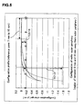
- Measurement results of the configurations of the obtained wafers were compensated such that a region of between 7 mm and 10 mm away from the wafer outer periphery was set as a reference (zero) and plotted. At this time, an example of the obtained configuration profile is shown in FIG. 5 .
- TC3-10 a configuration change in the region of between 10 mm and 3 mm away from the wafer outer periphery was checked (expressed numerically). The obtained value will be called TC3-10 hereinafter. Similarly, a configuration change in a region of between 3 mm and 1 mm away from the wafer outer periphery is indicated by TC1-3.
- Oxide films each having a film thickness of 150 nm were then formed on the surfaces of the bond wafers on the respective levels through thermal oxidation.
- hydrogen ions were implanted to form a sealed layer. SPM cleaning and RCA cleaning were then performed to remove organic matter.
- the ion-implanted surface of the bond wafer was brought into close contact with the surface of the base wafer of the same level as that of the bond wafer at room temperature. Delaminating heat treatment was applied thereto at 500°C for 30 minutes in a nitrogen atmosphere to delaminate a part of the bond wafer to thereby make the bond wafer into a thin film, with the result that there was obtained an SOI layer having a thickness of about 250 nm.
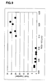
- Voids of the obtained SOI wafers were checked. A considerably large number of voids were generated in some wafers. In particular, a large number of voids were generated in vicinity of a position of 5 mm away from the wafer outer peripheries.
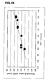
- TC1-3 a relationship between TC1-3 and the width of the unbonded region is shown in FIG. 10 .
- an SOI layer (a terrace portion) is formed to the outer peripheral portion of the substrate as this value becomes smaller.
- the unbonded region between the substrate and the SOI layer affects a configuration change of the outermost peripheral portion (about 1 to 3 mm).
- the configuration ranging from 3 mm away from the outer periphery to the center of the wafer affects a region in which voids are generated.
- the configuration of a specific area in the outer peripheral sag e.g., a region of between about 3 mm and 10 mm away from the outer periphery was especially a key element.
- an obtained result (a configuration profile) was subjected to a differential process to determine an inclination.
- SOI wafers were manufactured by the same method as that in Experimental Example 1 using, as starting wafers, wafers polished in a plurality of polishing steps, and differential profiles and generation statuses of voids were checked.
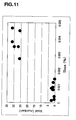
- a slope in a wafer where a considerably large number of voids are generated is larger than that in a wafer where a small number of voids are generated as shown in FIG. 8 , for example, at a position of 5 mm away from the outer periphery.
- a thick line indicates a wafer where voids are easily generated
- a dotted line indicates a wafer where voids were less generated.
- a position where an inclination is generated starts from the inside of a wafer.
- a silicon oxide film of 150 nm in thickness was formed on the surface (the entire surface) of the bond wafer by thermal oxidation. Hydrogen ions were implanted into the bond wafer to form a fine air bubble layer (a sealed layer). In addition, RCA cleaning and SPM cleaning to remove organic matter were performed.
- the oxide film on the surface of the bond wafer through which ions were implanted and the surface of the base wafer were brought into close contact with each other at room temperature.
- heat treatment (delaminating heat treatment) was applied thereto at 500°C or higher to delaminate a part of the bond wafer from the sealed layer thereof to thereby make the bond wafer into a thin film, with result that there was obtained an SOI layer.
- bonding heat treatment was applied thereto to strongly bond the SOI layer to the base wafer.
- heat treatment was applied in an argon gas atmosphere. This heat treatment was performed at 1200°C for 1 hour in an argon gas atmosphere using a vertical heater type heat treatment apparatus (batch furnace).
- the SOI layer was polished by a CMP polishing apparatus.
- the SOI layer was subjected to sacrifice oxidation to oxidize silicon in the SOI layer.
- the resultant SOI layer was treated with hydrofluoric acid to finally manufacture a thin-film SOI wafer including an SOI layer of about 150 nm.
- FIG. 12 shows results obtained by observing the outer peripheral portion of the SOI wafer manufactured in this example using a laser microscope with a confocal optical system. In this drawing, there was particularly observed in a magnified state a boundary (terrace portion) 62 between the SOI layer 52 and the support substrate 56 of the SOI wafer 50.
- voids 70 were observed in a portion away from the SOI layer 52 by a predetermined distance. However, in the wafers of this example, voids were rarely observed. Although voids were observed in wafer outer peripheral portions of four wafers, the numbers of voids were very small, i.e., 5 or less.
- FIG. 15 shows results obtained by observing the outer peripheral portion of the SOI wafer manufactured in this comparative example using a laser microscope with a confocal optical system. In this drawing, there was particularly observed in a magnified state a boundary (terrace portion) 62 between the SOI layer 52 and the support substrate 56 of the SOI wafer 50.
- Voids 70 were observed in a portion away from the SOI layer 52 by a predetermined distance, e.g., a wafer outer peripheral portion (a position of about 5 mm away from the outer periphery, FIG. 15(b) : a position of 145.1 mm away from the center, FIG. 15(c) : a position of 145.4 mm away from the center, FIG. 15(d) : and a position 144.9 mm away from the center).
- the numbers of voids were 20 or more, and voids were densely observed at positions opposing notches.
- the manufacturing processes described in the above examples are presented by way of illustration only.
- the method for manufacturing an SOI wafer includes the ion-implantation step and the adhering step
- the present invention may employ addition of various steps such as cleaning and heat treatment other than the above steps.
- the steps of controlling the thickness of an SOI layer of an SOI structure the present invention may adopt proper changes of the steps depending on purposes, for example, a partial change for the order of the steps, and partial omission for the steps such as CMP polishing.
- the number of voids generated in a wafer outer peripheral portion remarkably decreases, and it is possible to manufacture an SOI wafer with a good product yield and high productivity.
Landscapes
- Element Separation (AREA)
- Mechanical Treatment Of Semiconductor (AREA)
Claims (3)
- Procédé de fabrication d'une plaquette de SOI (50) comprenant les étapes consistant à :former une couche d'isolation (54a) sur au moins une plaquette de deux plaquettes d'amorçage (52a, 56a) ; etcoller la première plaquette sur l'autre plaquette sans utiliser d'adhésif,caractérisé en ce qu'on utilise en tant que plaquette d'amorçage une plaquette ayant une configuration périphérique externe avec une variation d'épaisseur contrôlée inférieure ou égale à 0,1 µm dans une région éloignée de 10 mm à 3 mm de la périphérie externe des plaquettes d'amorçage, dans lequel la périphérie externe correspond au périmètre des plaquettes d'amorçage.
- Procédé de fabrication d'une plaquette de SOI selon la revendication 1,
dans lequel on utilise en tant que plaquettes d'amorçage chacune des plaquettes ayant une configuration périphérique externe avec une pente inférieure ou égale à 0,002 % dans une position éloignée de 5 mm de la périphérie externe des plaquettes d'amorçage. - Procédé de fabrication d'une plaquette de SOI selon la revendication 1, dans lequel le procédé comprend en outre les étapes consistant à :implanter des ions d'hydrogène ou des ions de gaz rare à travers la surface supérieure de la première plaquette pour former une couche de microbulles à l'intérieur de la première plaquette ;amener ensuite la surface de la première plaquette à travers laquelle les ions ont été implantés en contact étroit avec l'autre plaquette par l'intermédiaire de la couche isolante intercalée entre elles ; puisdécoller une partie de la première plaquette avec la couche de microbulles en tant que plan de clivage en appliquant un traitement thermique pour que le reste de celle-ci devienne un film mince ; etlier fortement la première plaquette sous forme d'un film mince à l'autre plaquette par l'intermédiaire de la couche isolante intercalée entre elles en appliquant un autre traitement thermique.
Applications Claiming Priority (3)
| Application Number | Priority Date | Filing Date | Title |
|---|---|---|---|
| JP2002348610A JP2004186226A (ja) | 2002-11-29 | 2002-11-29 | Soiウエーハの製造方法 |
| JP2002348610 | 2002-11-29 | ||
| PCT/JP2003/014442 WO2004051715A1 (fr) | 2002-11-29 | 2003-11-13 | Procede servant a fabriquer une tranche de silicium sur isolant |
Publications (3)
| Publication Number | Publication Date |
|---|---|
| EP1566830A1 EP1566830A1 (fr) | 2005-08-24 |
| EP1566830A4 EP1566830A4 (fr) | 2010-03-03 |
| EP1566830B1 true EP1566830B1 (fr) | 2015-05-06 |
Family
ID=32462928
Family Applications (1)
| Application Number | Title | Priority Date | Filing Date |
|---|---|---|---|
| EP20030774018 Expired - Lifetime EP1566830B1 (fr) | 2002-11-29 | 2003-11-13 | Procede servant a fabriquer une tranche de silicium sur isolant |
Country Status (5)
| Country | Link |
|---|---|
| US (1) | US7435662B2 (fr) |
| EP (1) | EP1566830B1 (fr) |
| JP (1) | JP2004186226A (fr) |
| TW (1) | TW200423216A (fr) |
| WO (1) | WO2004051715A1 (fr) |
Families Citing this family (16)
| Publication number | Priority date | Publication date | Assignee | Title |
|---|---|---|---|---|
| US6926829B2 (en) | 2000-03-06 | 2005-08-09 | Kvaerner Process Systems A.S. | Apparatus and method for separating fluids through a membrane |
| US7501303B2 (en) * | 2001-11-05 | 2009-03-10 | The Trustees Of Boston University | Reflective layer buried in silicon and method of fabrication |
| WO2004073057A1 (fr) * | 2003-02-14 | 2004-08-26 | Sumitomo Mitsubishi Silicon Corporation | Procede de fabrication d'une tranche de silicium |
| US7601271B2 (en) | 2005-11-28 | 2009-10-13 | S.O.I.Tec Silicon On Insulator Technologies | Process and equipment for bonding by molecular adhesion |
| JP4951949B2 (ja) * | 2005-12-05 | 2012-06-13 | 株式会社Sumco | 貼合せ基板の製造方法 |
| EP1840955B1 (fr) * | 2006-03-31 | 2008-01-09 | S.O.I.TEC. Silicon on Insulator Technologies S.A. | Méthode de fabrication d'un matériau composite et méthode de sélection d'une plaquette |
| JP2008028070A (ja) * | 2006-07-20 | 2008-02-07 | Sumco Corp | 貼り合わせウェーハの製造方法 |
| KR101460993B1 (ko) * | 2007-01-31 | 2014-11-13 | 신에쯔 한도타이 가부시키가이샤 | 실리콘 웨이퍼의 면취 장치 및 실리콘 웨이퍼의 제조방법 그리고 에치드 실리콘 웨이퍼 |
| FR2938202B1 (fr) * | 2008-11-07 | 2010-12-31 | Soitec Silicon On Insulator | Traitement de surface pour adhesion moleculaire |
| JP2010245411A (ja) * | 2009-04-09 | 2010-10-28 | Hitachi Ltd | 半導体装置 |
| US8377825B2 (en) * | 2009-10-30 | 2013-02-19 | Corning Incorporated | Semiconductor wafer re-use using chemical mechanical polishing |
| US8562849B2 (en) * | 2009-11-30 | 2013-10-22 | Corning Incorporated | Methods and apparatus for edge chamfering of semiconductor wafers using chemical mechanical polishing |
| US8330245B2 (en) * | 2010-02-25 | 2012-12-11 | Memc Electronic Materials, Inc. | Semiconductor wafers with reduced roll-off and bonded and unbonded SOI structures produced from same |
| US9156705B2 (en) | 2010-12-23 | 2015-10-13 | Sunedison, Inc. | Production of polycrystalline silicon by the thermal decomposition of dichlorosilane in a fluidized bed reactor |
| FR2990054B1 (fr) | 2012-04-27 | 2014-05-02 | Commissariat Energie Atomique | Procede de collage dans une atmosphere de gaz presentant un coefficient de joule-thomson negatif. |
| JP6531743B2 (ja) * | 2016-09-27 | 2019-06-19 | 信越半導体株式会社 | 貼り合わせsoiウェーハの製造方法 |
Family Cites Families (9)
| Publication number | Priority date | Publication date | Assignee | Title |
|---|---|---|---|---|
| JP2675691B2 (ja) * | 1991-05-22 | 1997-11-12 | 信越半導体株式会社 | 半導体素子形成用基板の製造方法 |
| JP2959704B2 (ja) * | 1995-03-27 | 1999-10-06 | 信越半導体株式会社 | 結合ウェーハの製造方法及びこの方法により製造された結合ウェーハ |
| JPH09232197A (ja) * | 1996-02-27 | 1997-09-05 | Sumitomo Sitix Corp | 貼り合わせ半導体ウエーハの製造方法 |
| US6534380B1 (en) * | 1997-07-18 | 2003-03-18 | Denso Corporation | Semiconductor substrate and method of manufacturing the same |
| JP2001326197A (ja) * | 2000-03-10 | 2001-11-22 | Mitsubishi Materials Silicon Corp | 半導体ウェーハの研磨方法およびその装置 |
| JP4846915B2 (ja) * | 2000-03-29 | 2011-12-28 | 信越半導体株式会社 | 貼り合わせウェーハの製造方法 |
| EP1189266B1 (fr) | 2000-03-29 | 2017-04-05 | Shin-Etsu Handotai Co., Ltd. | Procede d'obtention de tranches de silicium ou de soi et tranches ainsi obtenues |
| JP2001328062A (ja) * | 2000-05-22 | 2001-11-27 | Mitsubishi Materials Silicon Corp | 半導体ウェーハの研磨方法およびその装置 |
| JP2001338899A (ja) * | 2000-05-26 | 2001-12-07 | Shin Etsu Handotai Co Ltd | 半導体ウエーハの製造方法及び半導体ウエーハ |
-
2002
- 2002-11-29 JP JP2002348610A patent/JP2004186226A/ja active Pending
-
2003
- 2003-11-13 WO PCT/JP2003/014442 patent/WO2004051715A1/fr not_active Ceased
- 2003-11-13 EP EP20030774018 patent/EP1566830B1/fr not_active Expired - Lifetime
- 2003-11-13 US US10/536,428 patent/US7435662B2/en not_active Expired - Lifetime
- 2003-11-21 TW TW092132781A patent/TW200423216A/zh not_active IP Right Cessation
Also Published As
| Publication number | Publication date |
|---|---|
| TW200423216A (en) | 2004-11-01 |
| WO2004051715A1 (fr) | 2004-06-17 |
| EP1566830A1 (fr) | 2005-08-24 |
| EP1566830A4 (fr) | 2010-03-03 |
| US20060024915A1 (en) | 2006-02-02 |
| US7435662B2 (en) | 2008-10-14 |
| TWI313483B (fr) | 2009-08-11 |
| JP2004186226A (ja) | 2004-07-02 |
Similar Documents
| Publication | Publication Date | Title |
|---|---|---|
| EP1566830B1 (fr) | Procede servant a fabriquer une tranche de silicium sur isolant | |
| US6596610B1 (en) | Method for reclaiming delaminated wafer and reclaimed delaminated wafer | |
| US7276427B2 (en) | Method for manufacturing SOI wafer | |
| US8557679B2 (en) | Oxygen plasma conversion process for preparing a surface for bonding | |
| EP2589074A1 (fr) | Semi-conducteur sur substrat de verre à couche de raidissage et son procédé de fabrication | |
| KR20100080777A (ko) | 열 처리를 사용하는 박리 과정에서 반도체 웨이퍼 재-사용 | |
| US7312154B2 (en) | Method of polishing a semiconductor-on-insulator structure | |
| EP1981063B1 (fr) | Procede de production de tranches soi | |
| US8703580B2 (en) | Silicon on insulator (SOI) wafer and process for producing same | |
| EP1654758A1 (fr) | Procede de production de couches minces d'un materiau semi-conducteur a partir d'une tranche du type donneur a double face | |
| EP1548822A1 (fr) | Procede de fabrication de plaquette silicium sur isolant | |
| KR20040060990A (ko) | 접합 웨이퍼의 제조 방법 | |
| US7291055B2 (en) | Wafer polishing method and apparatus | |
| KR940010159B1 (ko) | 반도체 기판의 제조 방법 | |
| CN116868308A (zh) | 贴合晶圆用支撑基板的制造方法及贴合晶圆用支撑基板 | |
| JP2001217253A (ja) | Soiウェーハ及び半導体単結晶ウェーハ並びにそれらの製造方法 | |
| JPH08115918A (ja) | 単結晶シリコンウェーハの製造方法および単結晶シリコンウェーハ | |
| JPH11195774A (ja) | 半導体基板の作成方法 |
Legal Events
| Date | Code | Title | Description |
|---|---|---|---|
| PUAI | Public reference made under article 153(3) epc to a published international application that has entered the european phase |
Free format text: ORIGINAL CODE: 0009012 |
|
| 17P | Request for examination filed |
Effective date: 20050525 |
|
| AK | Designated contracting states |
Kind code of ref document: A1 Designated state(s): AT BE BG CH CY CZ DE DK EE ES FI FR GB GR HU IE IT LI LU MC NL PT RO SE SI SK TR |
|
| RBV | Designated contracting states (corrected) |
Designated state(s): DE FR |
|
| RAP1 | Party data changed (applicant data changed or rights of an application transferred) |
Owner name: SHIN-ETSU HANDOTAI CO., LTD. |
|
| A4 | Supplementary search report drawn up and despatched |
Effective date: 20100128 |
|
| 17Q | First examination report despatched |
Effective date: 20100504 |
|
| GRAP | Despatch of communication of intention to grant a patent |
Free format text: ORIGINAL CODE: EPIDOSNIGR1 |
|
| RIC1 | Information provided on ipc code assigned before grant |
Ipc: H01L 21/02 20060101AFI20141107BHEP Ipc: H01L 21/762 20060101ALI20141107BHEP |
|
| INTG | Intention to grant announced |
Effective date: 20141211 |
|
| GRAS | Grant fee paid |
Free format text: ORIGINAL CODE: EPIDOSNIGR3 |
|
| GRAA | (expected) grant |
Free format text: ORIGINAL CODE: 0009210 |
|
| AK | Designated contracting states |
Kind code of ref document: B1 Designated state(s): DE FR |
|
| REG | Reference to a national code |
Ref country code: DE Ref legal event code: R096 Ref document number: 60347608 Country of ref document: DE Effective date: 20150625 |
|
| REG | Reference to a national code |
Ref country code: FR Ref legal event code: PLFP Year of fee payment: 13 |
|
| REG | Reference to a national code |
Ref country code: DE Ref legal event code: R097 Ref document number: 60347608 Country of ref document: DE |
|
| PLBE | No opposition filed within time limit |
Free format text: ORIGINAL CODE: 0009261 |
|
| STAA | Information on the status of an ep patent application or granted ep patent |
Free format text: STATUS: NO OPPOSITION FILED WITHIN TIME LIMIT |
|
| 26N | No opposition filed |
Effective date: 20160209 |
|
| REG | Reference to a national code |
Ref country code: FR Ref legal event code: PLFP Year of fee payment: 14 |
|
| REG | Reference to a national code |
Ref country code: FR Ref legal event code: PLFP Year of fee payment: 15 |
|
| REG | Reference to a national code |
Ref country code: FR Ref legal event code: PLFP Year of fee payment: 16 |
|
| PGFP | Annual fee paid to national office [announced via postgrant information from national office to epo] |
Ref country code: FR Payment date: 20221010 Year of fee payment: 20 |
|
| PGFP | Annual fee paid to national office [announced via postgrant information from national office to epo] |
Ref country code: DE Payment date: 20220930 Year of fee payment: 20 |
|
| REG | Reference to a national code |
Ref country code: DE Ref legal event code: R071 Ref document number: 60347608 Country of ref document: DE |