EP1573369B1 - Guide d'onde à l'enlargement de pupille avec réseau à diffraction pour equilibrer l'efficacité de diffraction - Google Patents
Guide d'onde à l'enlargement de pupille avec réseau à diffraction pour equilibrer l'efficacité de diffraction Download PDFInfo
- Publication number
- EP1573369B1 EP1573369B1 EP03778372.7A EP03778372A EP1573369B1 EP 1573369 B1 EP1573369 B1 EP 1573369B1 EP 03778372 A EP03778372 A EP 03778372A EP 1573369 B1 EP1573369 B1 EP 1573369B1
- Authority
- EP
- European Patent Office
- Prior art keywords
- grating
- epe
- substrate
- mbg
- light wave
- Prior art date
- Legal status (The legal status is an assumption and is not a legal conclusion. Google has not performed a legal analysis and makes no representation as to the accuracy of the status listed.)
- Expired - Lifetime
Links
- 210000001747 pupil Anatomy 0.000 title claims description 21
- 239000000758 substrate Substances 0.000 claims description 35
- 230000003287 optical effect Effects 0.000 claims description 22
- 230000007704 transition Effects 0.000 claims description 21
- 238000003384 imaging method Methods 0.000 claims description 7
- 230000003993 interaction Effects 0.000 claims description 5
- 230000001902 propagating effect Effects 0.000 claims 2
- 230000000694 effects Effects 0.000 claims 1
- XAGFODPZIPBFFR-UHFFFAOYSA-N aluminium Chemical compound [Al] XAGFODPZIPBFFR-UHFFFAOYSA-N 0.000 description 4
- 229910052782 aluminium Inorganic materials 0.000 description 4
- 239000004411 aluminium Substances 0.000 description 4
- 238000000576 coating method Methods 0.000 description 3
- 239000000463 material Substances 0.000 description 3
- 238000010276 construction Methods 0.000 description 2
- 230000008878 coupling Effects 0.000 description 2
- 238000010168 coupling process Methods 0.000 description 2
- 238000005859 coupling reaction Methods 0.000 description 2
- 238000004088 simulation Methods 0.000 description 2
- 230000000007 visual effect Effects 0.000 description 2
- 239000004606 Fillers/Extenders Substances 0.000 description 1
- 230000005540 biological transmission Effects 0.000 description 1
- 238000004364 calculation method Methods 0.000 description 1
- 230000008859 change Effects 0.000 description 1
- 230000003247 decreasing effect Effects 0.000 description 1
- 230000000593 degrading effect Effects 0.000 description 1
- 230000001419 dependent effect Effects 0.000 description 1
- 238000005516 engineering process Methods 0.000 description 1
- 238000007667 floating Methods 0.000 description 1
- 239000011521 glass Substances 0.000 description 1
- 210000003128 head Anatomy 0.000 description 1
- 239000004973 liquid crystal related substance Substances 0.000 description 1
- 238000004519 manufacturing process Methods 0.000 description 1
- 230000003134 recirculating effect Effects 0.000 description 1
- 238000002310 reflectometry Methods 0.000 description 1
- 229910052710 silicon Inorganic materials 0.000 description 1
- 239000010703 silicon Substances 0.000 description 1
Images






Classifications
-
- G—PHYSICS
- G02—OPTICS
- G02B—OPTICAL ELEMENTS, SYSTEMS OR APPARATUS
- G02B27/00—Optical systems or apparatus not provided for by any of the groups G02B1/00 - G02B26/00, G02B30/00
- G02B27/0081—Optical systems or apparatus not provided for by any of the groups G02B1/00 - G02B26/00, G02B30/00 with means for altering, e.g. enlarging, the entrance or exit pupil
-
- G—PHYSICS
- G02—OPTICS
- G02B—OPTICAL ELEMENTS, SYSTEMS OR APPARATUS
- G02B27/00—Optical systems or apparatus not provided for by any of the groups G02B1/00 - G02B26/00, G02B30/00
- G02B27/09—Beam shaping, e.g. changing the cross-sectional area, not otherwise provided for
- G02B27/0938—Using specific optical elements
- G02B27/0944—Diffractive optical elements, e.g. gratings, holograms
-
- G—PHYSICS
- G02—OPTICS
- G02B—OPTICAL ELEMENTS, SYSTEMS OR APPARATUS
- G02B5/00—Optical elements other than lenses
- G02B5/18—Diffraction gratings
- G02B5/1842—Gratings for image generation
-
- G—PHYSICS
- G02—OPTICS
- G02B—OPTICAL ELEMENTS, SYSTEMS OR APPARATUS
- G02B5/00—Optical elements other than lenses
- G02B5/32—Holograms used as optical elements
-
- G—PHYSICS
- G02—OPTICS
- G02B—OPTICAL ELEMENTS, SYSTEMS OR APPARATUS
- G02B6/00—Light guides; Structural details of arrangements comprising light guides and other optical elements, e.g. couplings
- G02B6/10—Light guides; Structural details of arrangements comprising light guides and other optical elements, e.g. couplings of the optical waveguide type
- G02B6/12—Light guides; Structural details of arrangements comprising light guides and other optical elements, e.g. couplings of the optical waveguide type of the integrated circuit kind
- G02B2006/12083—Constructional arrangements
- G02B2006/12107—Grating
Definitions
- the present invention relates to a diffractive grating element according to the preamble of the appended claim 1.
- Display technology is one of the key elements in the development of new portable devices, which today typically feature wireless connectivity for voice and data access - and that will include a display for viewing, for example, text, graphics and different types of multimedia.
- the displays of such portable devices need to be increasingly capable of reproducing high quality still images and also live video.
- Such devices include, for example, advanced mobile phones and portable Internet appliances.
- Microdisplay-based systems may be generally defined as systems where the image produced by an image source has to be magnified for viewing. Generally, such microdisplay-based systems are driven by small, high-resolution integrated circuit display chips, but other configurations are possible too.
- Microdisplays offer designers a chance to increase the displayed image size and resolution, yet physically shrink the size of the image source itself. In many cases, the smaller the image source, the lower the cost. So, not only do microdisplays promise to lower system costs, but their physically smaller size will mean less bulky and heavy products and smaller power consumption, that is they will operate longer with the same battery source. With a microdisplay-based system high pixel densities may be achieved. Many direct view flat-panel displays for instance, produce full colour pixels at only 3-4 lines/mm. Many microdisplay-based systems can provide full colour pixels at 50-100 lines per mm.
- Microdisplay-based systems can be generally divided into two classes: projection display systems and virtual display systems.
- Projection display systems create a real image on a screen. Suitable imaging optics magnify and project an image that is created on a display chip embedded within a projector.
- Virtual microdisplay-based systems also use imaging optics to magnify an image, but to create a virtual image instead of a projected real image.
- a virtual image is what one sees when looking in an electronic viewfinder of a digital video camera, for example.
- the virtual image appears to be larger and floating at some distance from the eye of the observer - even though it is created by a small sized integrated display chip acting as the image source. In other words, the viewer has the illusion of seeing the source image as if he/she stands a certain distance away in front of a larger display monitor.
- Virtual displays which are kept close to the eye, can be monocular or biocular.
- One type of virtual displays are, for example, Head Up Displays (HUDs), where the imaging optics are located somewhat further away from the eye.
- HUDs Head Up Displays
- exit pupil diameter of the system An important and well-known aspect in virtual display devices, as also in many other optical systems, is the exit pupil diameter of the system.
- the diameter and also the location of the exit pupil are of considerable practical importance defining largely the overall usability of the virtual display device.
- the observer's eye needs to be positioned at the centre of the exit pupil located behind the optical system in order to see the image with full field-of-view.
- the exit pupil is like a window, through which the virtual image can be seen.
- the distance between the location of the exit pupil and the last optical component, for example, the eye-piece lens of a visual instrument is called eye relief.
- the eye relief together with the exit pupil, defines the freedom of observation, i.e. the volume where the observer's eye can be located with respect to the optical system.
- the current invention is especially related to such virtual display systems, where diffractive grating elements are used as a part of the imaging optics in order to create an enlarged virtual image from the smaller sized real image created by an image source, herein referred to as an imager, which is typically an integrated circuit display chip.
- an imager which is typically an integrated circuit display chip.
- the invention is not limited only to microdisplay-based systems, but can also be used in other virtual display systems. Besides display systems, the invention may in its generic form be utilized in other type of optical systems as well, where diffractive grating elements are used for expanding the exit pupil of the optical system.
- patent publication WO 99/52002 discloses optical devices, in which a plurality of holographic optical elements (HOEs), i.e. diffractive grating elements are arranged on a common planar light-transmittive substrate.
- HOEs holographic optical elements
- the disclosed devices may be used for magnifying the exit pupil of the imaging optics, which produces a virtual image at infinity from a real image source, and to further reflect this virtual image into the eye of an observer.
- EPEs exit pupil extenders
- Grating couplers in waveguide substrate as such are also well known in the art.
- Such grating couplers can comprise gratings with an asymmetric grating profile and two different regions arranged on opposite sides of a transition point (see e.g. DE3522849 ).
- the main purpose of the current invention is to present a novel solution for decreasing or eliminating completely the above explained angular dependency of the diffraction efficiency in a diffractive grating element.
- the invention is especially suitable for beam expansion purposes for example in EPEs and virtual display devices.
- a specific aim of the invention is to make possible to construct biocular and also monocular virtual display systems, where light can be uniformly distributed over the whole area of the exit pupil of the display in order to achieve high image quality.
- the diffractive grating element according to the invention is primarily characterized in what will be presented in the characterizing part of the independent claim 1.
- the dependent claims describe further some preferred embodiments of the invention.
- the basic idea of the invention is to substitute a continuous diffractive grating element or structure having a grating profile extending in an unchangeably, substantially continuous manner over the whole area where the incoming beam interacts with said grating, with a grating structure experiencing a transition in the grating profile typically within said area of interaction.
- said transition in the grating profile takes place substantially in the center of said area of interaction, i.e. substantially in the location where the optical axis of the incoming beam passes through the grating.
- a grating element according to the invention is referred shortly to as a "splitted grating".
- the point where the transition of the grating profile takes place, i.e. the point where the grating is "splitted” is referred to as the "transition point”.
- the angular dependency of a diffractive grating can be effectively compensated or eliminated using a splitted, preferably blazed grating together with input optics that have a certain beam offset as a function of the input angle.
- the diffractive grating element according to the invention is divided into at least two different grating regions each having different diffractive properties and arranged on opposite sides respect to the transition point to form a splitted grating structure.
- the diffractions generated by said at least two different grating regions are arranged to mutually compensate for the variation in the input angle of the incident light wave to the total diffraction efficiency of the at least one diffracted light wave that is arranged to propagate within said substrate.
- the grating element is arranged to be symmetrically splitted, i.e. the grating period profiles of the two different sides of the grating are arranged to be substantially mirror images of each other respect to transition point. Further, the grating profile in each of said sides is preferably a blazed type profile.
- the transition point is substantially outside the beam area, and the splitting is not symmetrical, as will be shown later. Therefore, the first interaction of the incident beam with the splitted grating element is arranged to take place substantially within a single grating region
- the less intense diffracted beam, R -1 is recirculated towards the original direction of R +1 beam. The intensity of said right hand side travelling beam is thus increased and its intensity is then substantially independent of incoming angle.
- One specific object of the invention is thus to allow to manufacture virtual display devices with significantly larger exit pupil diameter than prior art solutions without degrading the image quality. Along with larger exit pupil diameters, also a significantly larger eye relief can be achieved.
- Figure 6 illustrates schematically a preferred embodiment according to the invention.
- a grating profile with asymmetrical period profile in this particular example with a blazed period profile, is splitted symmetrically respect to a transition point TP into left BG left and right BG right sides to form a splitted grating element SG.
- the left BG left and right BG right sides of the grating are mirror images of each other respect to said transition point TP.
- the transition point TP is arranged on the point where the optical axis A of the incoming beam passes through the grating surface.
- R- 1,left is generated from the first order diffraction towards left from the left side BG left of the grating.
- R +1,left is generated from the first order diffraction towards right from the same left side BG left of the grating.
- the input angle ⁇ has a negative value
- R +1,left diffraction is stronger compared to R -1,left diffraction.
- the right side BG right of the grating creates diffraction R -1,right to the left and R +1,right to the right.
- R +1,right diffraction is weaker compared to R -1,right diffraction. Because of the splitted construction of the grating SG, the total diffraction towards left and right are substantially equal : R -1,left summed up together with R -1,right equals substantially in intensity compared to R +1,left summed up together with R +1,right .
- the different sides BG left , BG right of the splitted grating element SG are arranged to mutually compensate for the variation in the input angle ( ⁇ ) of the incident light wave (W).
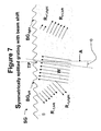
- Figure 7 illustrates schematically what happens when the beam incident to the splitted grating element SG shifts with respect to the transition point TP.
- the relative amount of diffraction generated by the left BG left and the right BG right side of the grating changes, but still R -1,left summed up together with R -1,right equals substantially in intensity compared to R +1,left summed up together with R +1,right .
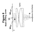
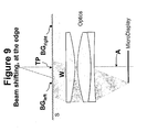
- Figure 8 illustrates schematically one possible optical setup for directing the light from an imager, for example from a microdisplay chip, towards the splitted grating element SG.
- Figure 8 presents schematically how light from an image point located in the center of the imager surface is directed towards the grating through the ocular type optics.
- Fig. 9 presents the case where an image point is located near the edge of the imager surface. It is evident for a person skilled in the art that when the image point "moves" from the center of the image surface towards the edge of the same, also the input angle of the light incident on the grating changes together with the relative area of the beam hitting the two regions BG left , BG right of the splitted grating element SG. However, according to the invention the total diffraction towards left (R -1,left + R -i,right ) and right (R +1,left + R +1,right ) directions along the substrate S are maintained substantially equal.
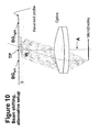
- Figure 10 illustrates an alternative optical setup for directing the light from an imager towards the splitted grating structure BG left , BG right .
- the ratio of R -1 and R +1 diffraction efficiencies becomes inversed. Therefore, for an off-centered image point the beam incident on the grating can be allowed to "cross" the center optical axis A and still be generating well balanced diffraction towards the left and right directions along the substrate S.
- Figure 11 shows simulation results for an aluminium coated splitted grating element SG having blazed period profile and corresponding basically to the arrangement shown in Fig. 6 .
- Figure 12 describes schematically how a splitted grating element SG according to the invention can be utilized in a monocular EPE.
- the first interaction of the incident light wave (W) with the splitted grating element SG is arranged to take place substantially within a single grating region MBG right .
- the splitted grating element SG comprises on the right side a grating surface MBG right optimized to generate first order diffraction R +1,right towards right along substrate S.
- the grating surface MBG left is optimized to generate a second order diffraction R +2,left towards right along substrate S.
- the aforementioned construction provides effective "recirculation" of the R 1,right diffraction "leaking" undesirably from MBG right towards left along substrate S. Namely, based on Bragg reflection grating surface MBG left diffracts R -1,right back towards right as R +2,left . It can be shown that this "recirculated" beam R +2,left is completely parallel respect to the beam R +1 , right . Therefore, if the input angle ⁇ of the beam incident to the right grating surface MBG right changes altering the ratio of R -1,right and R +1,right reflections and the amount of light "leaking" towards right along the substrate S, the splitted grating structure is capable of recirculating the light travelling in the opposite direction than desired.
- Figures 13a and 13b show how the coupling/diffraction efficiency of the grating surfaces MBG right and MBG left shown schematically in Fig. 12 depend on the depth of said grating profiles.
- the period of the gratings is given a value of 440 nm and the calculations have been performed for light having wavelength of 540 nm with refractive index of 1.71.
- Fig. 13a it can be seen that for the Bragg reflection (46.4°) the efficiency of the left grating MBG left can be optimized to have almost value of one, i.e. the grating reflects essentially all of the light back towards direction R +2 .
- Figure 13b corresponds to diffraction of a beam entering the substrate S plate substantially in perpendicular direction, i.e. corresponding MBG right in Fig. 12 .
- the preferred applications of the invention include different type of virtual display devices, where beam expansion in one or more directions is performed to extend the exit pupil of the display device.
- the image source can be, for example, a sequential colour LCOS-device (Liquid Crystal On Silicon), an OLED-device (Organic Light Emitting Diode), a MEMS-device (MicroElectroMechanical System) or any other suitable microdisplay device operating in transmission, reflection or emission.
- the exact grating profiles, grating periods or grating profile depths of the splitted grating element SG may be selected according to the specific application or materials utilized.
- the splitted grating element it is possible to use diffractive grating regions where the diffraction efficiency varies locally, for example, by arranging the depth of the grating region to be different at different local distances measured from the transition point TP.
- the change in the grating profile when moving over the transition point TP may be abrupt, as in the given examples, but it may also arranged to take place in a more smooth manner.
- blazed grating profiles are used, but other types of grating profiles may also be used.
- the grating profiles on one side of the transition point TP may thus be blazed, sinusoidal, height changing or of any other suitable type.
- the substrate S material may be, for example, glass or plastic or other suitable light-transmittive material.
- the grating structure may be arranged substantially on the surface of the substrate or it may also be embedded within the substrate as a buried structure.
- the substrate S is planar, but it also possible to use other forms of substrate which offer suitable waveguiding properties.
- the gratings or other areas of the substrate S may have suitable coatings, for example aluminium coatings, to enhance the reflectivity. It is also possible to use antireflection coatings if necessary.
- the applications of the invention may include, for example, portable Internet appliances, hand-held computers, personal digital assistant devices (PDAs) advanced mobile phones and other mobile stations, digital video and still cameras, wearable computers, computer game devices, specialized bring-to-the-eye products for viewing different types of information or presentations, and other devices including high quality virtual display devices.
- PDAs personal digital assistant devices
- the invention may also used in other applications than virtual displays.
- the invention is suitable to be used in any application where optical beam expansion in one or more directions is required.
- the invention can be applied to different type of optical couplers or other light modulator devices as well.
Landscapes
- Physics & Mathematics (AREA)
- General Physics & Mathematics (AREA)
- Optics & Photonics (AREA)
- Diffracting Gratings Or Hologram Optical Elements (AREA)
- Transforming Electric Information Into Light Information (AREA)
Claims (11)
- Dispositif (EPE) pour élargir une pupille de sortie d'un afficheur virtuel pour regarder des graphiques, la pupille de sortie de l'optique d'imagerie dudit afficheur virtuel étant disposée pour produire une image virtuelle à l'infini, ledit dispositif (EPE) comprenant un substrat guide d'ondes, et un premier élément de réseau de diffraction (SG) disposé sur ou incorporé à l'intérieur dudit substrat guide d'ondes (S), ledit premier élément de réseau de diffraction (SG) étant disposé pour interagir avec une onde lumineuse incidente (W) afin de coupler l'énergie de ladite onde lumineuse incidente (W) dans ledit substrat (S) pour former au moins une onde lumineuse diffractée (R-1, R+1) se propageant à l'intérieur dudit substrat (S) dans une direction d'un ordre de diffraction sélectionné, caractérisé en ce que ledit premier élément de réseau (SG) comprend au moins deux régions de réseau (BGgauche, BGdroite ; MBGgauche, MBGdroite) ayant des propriétés de diffraction différentes et disposées sur des côtés opposés par rapport à un point de transition (TP) de manière à compenser mutuellement un effet de variation de l'angle d'entrée (θ) de ladite onde lumineuse incidente (W) sur l'efficacité de diffraction totale de ladite au moins une onde lumineuse diffractée (R-1, R+1) se propageant à l'intérieur dudit substrat (S), l'une au moins desdites régions de réseau (BGgauche, BGdroite ; MBGgauche, MBGdroite) ayant un profil de période asymétrique.
- Dispositif (EPE) selon la revendication 1, caractérisé en ce que le profil de réseau d'au moins une des régions de réseau (BGgauche, BGdroite ; MBGgauche, MBGdroite) a un profil de période blazé.
- Dispositif (EPE) selon la revendication 1, caractérisé en ce que ledit premier élément de réseau (SG) comprend deux régions de réseau (BGgaucher BGdroite) dont les profils de période de réseau sont agencés pour être des images sensiblement miroirs l'un de l'autre par rapport au point de transition (TP).
- Dispositif (EPE) selon la revendication 1, caractérisé en ce que ledit premier élément de réseau (SG) comprend au moins deux régions de réseau (BGgauche, BGdroite) dont les profils de période de réseau ont des profondeurs sensiblement différentes.
- Dispositif (EPE) selon la revendication 1, caractérisé en ce que l'efficacité de diffraction d'au moins une des régions de réseau (BGgauche, BGdroite ; MBGgauche, MBGdroite) est disposée pour varier à différentes distances locales mesurées depuis le point de transition (TP).
- Dispositif (EPE) selon la revendication 1, caractérisé en ce que le point de transition (TP) est situé à l'intérieur d'une zone où l'onde lumineuse incidente (W) interagit pour la première fois avec ledit élément de réseau (SG).
- Dispositif (EPE) selon la revendication 1, caractérisé en ce que la première interaction de l'onde lumineuse incidente (W) avec ledit premier élément de réseau (SG) est disposée pour avoir lieu en grande partie à l'intérieur d'une seule région de réseau (MBGdroite).
- Dispositif (EPE) selon la revendication 7, caractérisé en ce qu'au moins une des régions de réseau (MBGgauche) est disposée pour rediriger ou refaire circuler l'onde lumineuse guidée à l'intérieur du substrat (S) dans une direction inverse à l'intérieur du substrat (S).
- Dispositif (EPE) selon la revendication 1, caractérisé en ce que le premier élément de réseau (SG) est disposé pour élargir la pupille de sortie d'un système optique binoculaire ou monoculaire.
- Dispositif (EPE) selon l'une quelconque des revendications 1 à 9 comprenant un deuxième élément de réseau de diffraction (DOE2) disposé pour coupler la lumière (R-1, R+1) guidée dans le substrat (S) en dehors dudit substrat (S) vers un volume où l'oeil de l'observateur peut être situé, pour regarder l'image virtuelle.
- Dispositif (EPE) selon l'une quelconque des revendications 1 à 10 comprenant un imageur, le premier élément de réseau de diffraction (SG, DOE1) étant disposé pour coupler la lumière provenant de l'imageur dans le substrat (S).
Applications Claiming Priority (3)
| Application Number | Priority Date | Filing Date | Title |
|---|---|---|---|
| FI20022199 | 2002-12-16 | ||
| FI20022199A FI114946B (fi) | 2002-12-16 | 2002-12-16 | Diffraktiivinen hilaelementti diffraktiohyötysuhteen tasapainottamiseksi |
| PCT/FI2003/000948 WO2004055556A1 (fr) | 2002-12-16 | 2003-12-12 | Element en reseau a diffraction pour equilibrer l'efficacite de diffraction |
Publications (2)
| Publication Number | Publication Date |
|---|---|
| EP1573369A1 EP1573369A1 (fr) | 2005-09-14 |
| EP1573369B1 true EP1573369B1 (fr) | 2014-07-09 |
Family
ID=8565081
Family Applications (1)
| Application Number | Title | Priority Date | Filing Date |
|---|---|---|---|
| EP03778372.7A Expired - Lifetime EP1573369B1 (fr) | 2002-12-16 | 2003-12-12 | Guide d'onde à l'enlargement de pupille avec réseau à diffraction pour equilibrer l'efficacité de diffraction |
Country Status (9)
| Country | Link |
|---|---|
| US (1) | US7483604B2 (fr) |
| EP (1) | EP1573369B1 (fr) |
| JP (1) | JP4510639B2 (fr) |
| KR (1) | KR100669162B1 (fr) |
| CN (1) | CN1726412B (fr) |
| AU (1) | AU2003285384A1 (fr) |
| FI (1) | FI114946B (fr) |
| PT (1) | PT1573369E (fr) |
| WO (1) | WO2004055556A1 (fr) |
Cited By (50)
| Publication number | Priority date | Publication date | Assignee | Title |
|---|---|---|---|---|
| US10089516B2 (en) | 2013-07-31 | 2018-10-02 | Digilens, Inc. | Method and apparatus for contact image sensing |
| US10145533B2 (en) | 2005-11-11 | 2018-12-04 | Digilens, Inc. | Compact holographic illumination device |
| US10156681B2 (en) | 2015-02-12 | 2018-12-18 | Digilens Inc. | Waveguide grating device |
| US10185154B2 (en) | 2011-04-07 | 2019-01-22 | Digilens, Inc. | Laser despeckler based on angular diversity |
| US10209517B2 (en) | 2013-05-20 | 2019-02-19 | Digilens, Inc. | Holographic waveguide eye tracker |
| US10216061B2 (en) | 2012-01-06 | 2019-02-26 | Digilens, Inc. | Contact image sensor using switchable bragg gratings |
| US10234696B2 (en) | 2007-07-26 | 2019-03-19 | Digilens, Inc. | Optical apparatus for recording a holographic device and method of recording |
| US10241330B2 (en) | 2014-09-19 | 2019-03-26 | Digilens, Inc. | Method and apparatus for generating input images for holographic waveguide displays |
| US10330777B2 (en) | 2015-01-20 | 2019-06-25 | Digilens Inc. | Holographic waveguide lidar |
| US10359736B2 (en) | 2014-08-08 | 2019-07-23 | Digilens Inc. | Method for holographic mastering and replication |
| US10409144B2 (en) | 2009-10-09 | 2019-09-10 | Digilens Inc. | Diffractive waveguide providing structured illumination for object detection |
| US10423222B2 (en) | 2014-09-26 | 2019-09-24 | Digilens Inc. | Holographic waveguide optical tracker |
| US10437064B2 (en) | 2015-01-12 | 2019-10-08 | Digilens Inc. | Environmentally isolated waveguide display |
| US10437051B2 (en) | 2012-05-11 | 2019-10-08 | Digilens Inc. | Apparatus for eye tracking |
| US10459145B2 (en) | 2015-03-16 | 2019-10-29 | Digilens Inc. | Waveguide device incorporating a light pipe |
| US10545346B2 (en) | 2017-01-05 | 2020-01-28 | Digilens Inc. | Wearable heads up displays |
| US10591756B2 (en) | 2015-03-31 | 2020-03-17 | Digilens Inc. | Method and apparatus for contact image sensing |
| US10642058B2 (en) | 2011-08-24 | 2020-05-05 | Digilens Inc. | Wearable data display |
| US10670876B2 (en) | 2011-08-24 | 2020-06-02 | Digilens Inc. | Waveguide laser illuminator incorporating a despeckler |
| US10678053B2 (en) | 2009-04-27 | 2020-06-09 | Digilens Inc. | Diffractive projection apparatus |
| US10690851B2 (en) | 2018-03-16 | 2020-06-23 | Digilens Inc. | Holographic waveguides incorporating birefringence control and methods for their fabrication |
| US10690916B2 (en) | 2015-10-05 | 2020-06-23 | Digilens Inc. | Apparatus for providing waveguide displays with two-dimensional pupil expansion |
| US10732569B2 (en) | 2018-01-08 | 2020-08-04 | Digilens Inc. | Systems and methods for high-throughput recording of holographic gratings in waveguide cells |
| US10859768B2 (en) | 2016-03-24 | 2020-12-08 | Digilens Inc. | Method and apparatus for providing a polarization selective holographic waveguide device |
| US10890707B2 (en) | 2016-04-11 | 2021-01-12 | Digilens Inc. | Holographic waveguide apparatus for structured light projection |
| US10914950B2 (en) | 2018-01-08 | 2021-02-09 | Digilens Inc. | Waveguide architectures and related methods of manufacturing |
| US10942430B2 (en) | 2017-10-16 | 2021-03-09 | Digilens Inc. | Systems and methods for multiplying the image resolution of a pixelated display |
| US10983340B2 (en) | 2016-02-04 | 2021-04-20 | Digilens Inc. | Holographic waveguide optical tracker |
| US11204540B2 (en) | 2009-10-09 | 2021-12-21 | Digilens Inc. | Diffractive waveguide providing a retinal image |
| US11307432B2 (en) | 2014-08-08 | 2022-04-19 | Digilens Inc. | Waveguide laser illuminator incorporating a Despeckler |
| US11378732B2 (en) | 2019-03-12 | 2022-07-05 | DigLens Inc. | Holographic waveguide backlight and related methods of manufacturing |
| US11402801B2 (en) | 2018-07-25 | 2022-08-02 | Digilens Inc. | Systems and methods for fabricating a multilayer optical structure |
| US11442222B2 (en) | 2019-08-29 | 2022-09-13 | Digilens Inc. | Evacuated gratings and methods of manufacturing |
| US11448937B2 (en) | 2012-11-16 | 2022-09-20 | Digilens Inc. | Transparent waveguide display for tiling a display having plural optical powers using overlapping and offset FOV tiles |
| US11480788B2 (en) | 2015-01-12 | 2022-10-25 | Digilens Inc. | Light field displays incorporating holographic waveguides |
| US11513350B2 (en) | 2016-12-02 | 2022-11-29 | Digilens Inc. | Waveguide device with uniform output illumination |
| US11543594B2 (en) | 2019-02-15 | 2023-01-03 | Digilens Inc. | Methods and apparatuses for providing a holographic waveguide display using integrated gratings |
| US11681143B2 (en) | 2019-07-29 | 2023-06-20 | Digilens Inc. | Methods and apparatus for multiplying the image resolution and field-of-view of a pixelated display |
| US11726332B2 (en) | 2009-04-27 | 2023-08-15 | Digilens Inc. | Diffractive projection apparatus |
| US11747568B2 (en) | 2019-06-07 | 2023-09-05 | Digilens Inc. | Waveguides incorporating transmissive and reflective gratings and related methods of manufacturing |
| EP4290294A1 (fr) | 2021-05-25 | 2023-12-13 | Shenzhen Optiark Semiconductor Technologies Limited | Appareil optique et dispositif d'affichage |
| US12092914B2 (en) | 2018-01-08 | 2024-09-17 | Digilens Inc. | Systems and methods for manufacturing waveguide cells |
| US12140764B2 (en) | 2019-02-15 | 2024-11-12 | Digilens Inc. | Wide angle waveguide display |
| US12158612B2 (en) | 2021-03-05 | 2024-12-03 | Digilens Inc. | Evacuated periodic structures and methods of manufacturing |
| US12210153B2 (en) | 2019-01-14 | 2025-01-28 | Digilens Inc. | Holographic waveguide display with light control layer |
| US12222499B2 (en) | 2020-12-21 | 2025-02-11 | Digilens Inc. | Eye glow suppression in waveguide based displays |
| US12306585B2 (en) | 2018-01-08 | 2025-05-20 | Digilens Inc. | Methods for fabricating optical waveguides |
| US12399326B2 (en) | 2021-01-07 | 2025-08-26 | Digilens Inc. | Grating structures for color waveguides |
| US12397477B2 (en) | 2019-02-05 | 2025-08-26 | Digilens Inc. | Methods for compensating for optical surface nonuniformity |
| US12596218B2 (en) | 2012-04-25 | 2026-04-07 | Digilens Inc. | Holographic wide angle display |
Families Citing this family (64)
| Publication number | Priority date | Publication date | Assignee | Title |
|---|---|---|---|---|
| WO2006064334A1 (fr) * | 2004-12-13 | 2006-06-22 | Nokia Corporation | Procede general d'optiques de diffraction pour prolongement de pupille de sortie |
| US20060126181A1 (en) | 2004-12-13 | 2006-06-15 | Nokia Corporation | Method and system for beam expansion in a display device |
| WO2007085682A1 (fr) | 2006-01-26 | 2007-08-02 | Nokia Corporation | Dispositif de poursuite oculaire |
| WO2007141587A1 (fr) | 2006-06-02 | 2007-12-13 | Nokia Corporation | Distribution de couleurs dans des expanseurs de pupilles de sortie |
| US8466953B2 (en) | 2006-06-02 | 2013-06-18 | Nokia Corporation | Stereoscopic exit pupil expander display |
| WO2007141588A1 (fr) | 2006-06-02 | 2007-12-13 | Nokia Corporation | Expanseur de pupille de sortie à substrat séparé |
| WO2008032879A1 (fr) * | 2006-09-15 | 2008-03-20 | Scalar Corporation | Prisme À surface incurvÉe libre, et casque de rÉALITÉ virtuelle |
| CN101512413B (zh) * | 2006-09-28 | 2012-02-15 | 诺基亚公司 | 利用三维衍射元件的光束扩展 |
| WO2008071830A1 (fr) * | 2006-12-14 | 2008-06-19 | Nokia Corporation | Dispositif d'affichage ayant deux modes de fonctionnement |
| WO2008134154A1 (fr) * | 2007-05-01 | 2008-11-06 | Pixeloptics, Inc. | Éléments optiques diffractifs à relief de surface assurant des pertes optiques réduites dans des lentilles électroactives comprenant des matériaux cristallins liquides |
| US8233204B1 (en) | 2009-09-30 | 2012-07-31 | Rockwell Collins, Inc. | Optical displays |
| US11320571B2 (en) | 2012-11-16 | 2022-05-03 | Rockwell Collins, Inc. | Transparent waveguide display providing upper and lower fields of view with uniform light extraction |
| US11300795B1 (en) | 2009-09-30 | 2022-04-12 | Digilens Inc. | Systems for and methods of using fold gratings coordinated with output couplers for dual axis expansion |
| JP5195707B2 (ja) * | 2009-09-30 | 2013-05-15 | ブラザー工業株式会社 | ヘッドマウントディスプレイ |
| US10795160B1 (en) | 2014-09-25 | 2020-10-06 | Rockwell Collins, Inc. | Systems for and methods of using fold gratings for dual axis expansion |
| US8659826B1 (en) | 2010-02-04 | 2014-02-25 | Rockwell Collins, Inc. | Worn display system and method without requiring real time tracking for boresight precision |
| US8634139B1 (en) | 2011-09-30 | 2014-01-21 | Rockwell Collins, Inc. | System for and method of catadioptric collimation in a compact head up display (HUD) |
| US9366864B1 (en) | 2011-09-30 | 2016-06-14 | Rockwell Collins, Inc. | System for and method of displaying information without need for a combiner alignment detector |
| US9507150B1 (en) | 2011-09-30 | 2016-11-29 | Rockwell Collins, Inc. | Head up display (HUD) using a bent waveguide assembly |
| US9715067B1 (en) | 2011-09-30 | 2017-07-25 | Rockwell Collins, Inc. | Ultra-compact HUD utilizing waveguide pupil expander with surface relief gratings in high refractive index materials |
| US9523852B1 (en) | 2012-03-28 | 2016-12-20 | Rockwell Collins, Inc. | Micro collimator system and method for a head up display (HUD) |
| US9674413B1 (en) | 2013-04-17 | 2017-06-06 | Rockwell Collins, Inc. | Vision system and method having improved performance and solar mitigation |
| US9244281B1 (en) | 2013-09-26 | 2016-01-26 | Rockwell Collins, Inc. | Display system and method using a detached combiner |
| US10732407B1 (en) | 2014-01-10 | 2020-08-04 | Rockwell Collins, Inc. | Near eye head up display system and method with fixed combiner |
| US9519089B1 (en) | 2014-01-30 | 2016-12-13 | Rockwell Collins, Inc. | High performance volume phase gratings |
| US9244280B1 (en) | 2014-03-25 | 2016-01-26 | Rockwell Collins, Inc. | Near eye display system and method for display enhancement or redundancy |
| CN104121990B (zh) * | 2014-07-22 | 2016-05-11 | 中国科学院上海光学精密机械研究所 | 基于随机光栅的压缩感知宽波段高光谱成像系统 |
| GB2529003B (en) * | 2014-08-03 | 2020-08-26 | Wave Optics Ltd | Optical device |
| US10088675B1 (en) | 2015-05-18 | 2018-10-02 | Rockwell Collins, Inc. | Turning light pipe for a pupil expansion system and method |
| US9715110B1 (en) | 2014-09-25 | 2017-07-25 | Rockwell Collins, Inc. | Automotive head up display (HUD) |
| US11726241B2 (en) * | 2015-01-26 | 2023-08-15 | Magic Leap, Inc. | Manufacturing for virtual and augmented reality systems and components |
| US11366316B2 (en) | 2015-05-18 | 2022-06-21 | Rockwell Collins, Inc. | Head up display (HUD) using a light pipe |
| US10247943B1 (en) | 2015-05-18 | 2019-04-02 | Rockwell Collins, Inc. | Head up display (HUD) using a light pipe |
| US10126552B2 (en) | 2015-05-18 | 2018-11-13 | Rockwell Collins, Inc. | Micro collimator system and method for a head up display (HUD) |
| US10108010B2 (en) | 2015-06-29 | 2018-10-23 | Rockwell Collins, Inc. | System for and method of integrating head up displays and head down displays |
| US9910276B2 (en) | 2015-06-30 | 2018-03-06 | Microsoft Technology Licensing, Llc | Diffractive optical elements with graded edges |
| US10670862B2 (en) * | 2015-07-02 | 2020-06-02 | Microsoft Technology Licensing, Llc | Diffractive optical elements with asymmetric profiles |
| US10038840B2 (en) | 2015-07-30 | 2018-07-31 | Microsoft Technology Licensing, Llc | Diffractive optical element using crossed grating for pupil expansion |
| US9864208B2 (en) | 2015-07-30 | 2018-01-09 | Microsoft Technology Licensing, Llc | Diffractive optical elements with varying direction for depth modulation |
| US10073278B2 (en) | 2015-08-27 | 2018-09-11 | Microsoft Technology Licensing, Llc | Diffractive optical element using polarization rotation grating for in-coupling |
| US10429645B2 (en) | 2015-10-07 | 2019-10-01 | Microsoft Technology Licensing, Llc | Diffractive optical element with integrated in-coupling, exit pupil expansion, and out-coupling |
| US10241332B2 (en) | 2015-10-08 | 2019-03-26 | Microsoft Technology Licensing, Llc | Reducing stray light transmission in near eye display using resonant grating filter |
| US9946072B2 (en) | 2015-10-29 | 2018-04-17 | Microsoft Technology Licensing, Llc | Diffractive optical element with uncoupled grating structures |
| US10234686B2 (en) | 2015-11-16 | 2019-03-19 | Microsoft Technology Licensing, Llc | Rainbow removal in near-eye display using polarization-sensitive grating |
| US10162181B2 (en) | 2015-12-03 | 2018-12-25 | Microsoft Technology Licensing, Llc | Display device with optics for brightness uniformity tuning having DOE optically coupled to receive light at central and peripheral regions |
| US10598932B1 (en) | 2016-01-06 | 2020-03-24 | Rockwell Collins, Inc. | Head up display for integrating views of conformally mapped symbols and a fixed image source |
| US10422508B2 (en) * | 2016-03-28 | 2019-09-24 | Kla-Tencor Corporation | System and method for spectral tuning of broadband light sources |
| US10067347B2 (en) | 2016-04-13 | 2018-09-04 | Microsoft Technology Licensing, Llc | Waveguides with improved intensity distributions |
| US9791703B1 (en) | 2016-04-13 | 2017-10-17 | Microsoft Technology Licensing, Llc | Waveguides with extended field of view |
| US10061124B2 (en) | 2016-04-29 | 2018-08-28 | Microsoft Technology Licensing, Llc | Robust architecture for large field of view components |
| US10241346B2 (en) | 2016-05-07 | 2019-03-26 | Microsoft Technology Licensing, Llc | Degrees of freedom for diffraction elements in wave expander |
| US10353202B2 (en) * | 2016-06-09 | 2019-07-16 | Microsoft Technology Licensing, Llc | Wrapped waveguide with large field of view |
| US10095045B2 (en) | 2016-09-12 | 2018-10-09 | Microsoft Technology Licensing, Llc | Waveguide comprising a bragg polarization grating |
| US11067860B2 (en) | 2016-11-18 | 2021-07-20 | Magic Leap, Inc. | Liquid crystal diffractive devices with nano-scale pattern and methods of manufacturing the same |
| KR102533671B1 (ko) | 2016-11-18 | 2023-05-16 | 매직 립, 인코포레이티드 | 공간 가변적 액정 회절 격자들 |
| US10108014B2 (en) * | 2017-01-10 | 2018-10-23 | Microsoft Technology Licensing, Llc | Waveguide display with multiple focal depths |
| US10295824B2 (en) | 2017-01-26 | 2019-05-21 | Rockwell Collins, Inc. | Head up display with an angled light pipe |
| US11141645B2 (en) | 2018-09-11 | 2021-10-12 | Real Shot Inc. | Athletic ball game using smart glasses |
| US11103763B2 (en) | 2018-09-11 | 2021-08-31 | Real Shot Inc. | Basketball shooting game using smart glasses |
| GB201903708D0 (en) * | 2019-03-19 | 2019-05-01 | Wave Optics Ltd | Improved angular uniformity waveguide for augmented or virtual reality |
| CN112731659B (zh) * | 2019-10-14 | 2024-12-31 | 苏州苏大维格科技集团股份有限公司 | 波导显示镜片及增强现实眼镜 |
| CN115151844B (zh) * | 2020-02-25 | 2024-01-16 | 华为技术有限公司 | 用于电子设备的成像系统 |
| WO2022086002A1 (fr) | 2020-10-20 | 2022-04-28 | Samsung Electronics Co., Ltd. | Structure de guide d'ondes à éléments optiques diffractifs segmentés et appareil d'affichage proche de l'œil l'utilisant |
| CN113625446B (zh) * | 2021-07-15 | 2024-02-02 | 嘉兴驭光光电科技有限公司 | Ar光波导的设计方法及用于ar眼镜的光波导 |
Citations (3)
| Publication number | Priority date | Publication date | Assignee | Title |
|---|---|---|---|---|
| DE3522849A1 (de) * | 1984-06-27 | 1986-01-02 | Canon Denshi K.K., Chichibu, Saitama | Optischer kopf |
| JPS6464156A (en) * | 1987-05-20 | 1989-03-10 | Ricoh Kk | Optical information recording and reproducing device |
| JPH03279811A (ja) * | 1990-03-29 | 1991-12-11 | Nikon Corp | エンコーダ |
Family Cites Families (20)
| Publication number | Priority date | Publication date | Assignee | Title |
|---|---|---|---|---|
| US4779259A (en) * | 1985-04-25 | 1988-10-18 | Mitsubishi Denki Kabushiki Kaisha | Optical head assembly with efficient light source coupling surface and method of construction |
| JP2539406B2 (ja) * | 1987-02-04 | 1996-10-02 | 株式会社日立製作所 | 固体光ピツクアツプ |
| JPH02188729A (ja) * | 1989-01-17 | 1990-07-24 | Sharp Corp | 光学素子の回析格子製造方法 |
| US5279924A (en) * | 1989-04-04 | 1994-01-18 | Sharp Kabushiki Kaisha | Manufacturing method of optical diffraction grating element with serrated gratings having uniformly etched grooves |
| KR930010473B1 (ko) * | 1989-09-22 | 1993-10-25 | 마쯔시다덴기산교 가부시기가이샤 | 편광소자 및 그것을 사용한 광학헤드장치 |
| US5224198A (en) * | 1991-09-30 | 1993-06-29 | Motorola, Inc. | Waveguide virtual image display |
| US6461544B1 (en) * | 1993-05-03 | 2002-10-08 | Crown Roll Leaf, Inc. | Two-dimensional/three-dimensional graphic material and method of making same |
| JPH10186120A (ja) | 1996-12-26 | 1998-07-14 | Canon Inc | 回折光学素子及びそれを有する光学系並びに光学機器 |
| JP3813693B2 (ja) * | 1997-06-24 | 2006-08-23 | オリンパス株式会社 | 画像表示装置 |
| US6285813B1 (en) * | 1997-10-03 | 2001-09-04 | Georgia Tech Research Corporation | Diffractive grating coupler and method |
| ATE254291T1 (de) * | 1998-04-02 | 2003-11-15 | Elop Electrooptics Ind Ltd | Optische holographische vorrichtungen |
| JP2000056259A (ja) * | 1998-08-10 | 2000-02-25 | Fuji Xerox Co Ltd | 画像表示装置 |
| US6728034B1 (en) * | 1999-06-16 | 2004-04-27 | Matsushita Electric Industrial Co., Ltd. | Diffractive optical element that polarizes light and an optical pickup using the same |
| US6598987B1 (en) | 2000-06-15 | 2003-07-29 | Nokia Mobile Phones Limited | Method and apparatus for distributing light to the user interface of an electronic device |
| JP4210425B2 (ja) * | 2000-12-08 | 2009-01-21 | 富士フイルム株式会社 | 光学素子 |
| TW522256B (en) | 2000-12-15 | 2003-03-01 | Samsung Electronics Co Ltd | Wearable display system |
| WO2003027754A1 (fr) * | 2001-09-25 | 2003-04-03 | Cambridge Flat Projection Displays | Affichage par projection a ecran plat |
| US7528385B2 (en) * | 2002-03-15 | 2009-05-05 | Pd-Ld, Inc. | Fiber optic devices having volume Bragg grating elements |
| US6805490B2 (en) * | 2002-09-30 | 2004-10-19 | Nokia Corporation | Method and system for beam expansion in a display device |
| FI115169B (fi) * | 2003-05-13 | 2005-03-15 | Nokia Corp | Menetelmä ja optinen järjestelmä valon kytkemiseksi aaltojohteeseen |
-
2002
- 2002-12-16 FI FI20022199A patent/FI114946B/fi not_active IP Right Cessation
-
2003
- 2003-12-12 KR KR1020057011005A patent/KR100669162B1/ko not_active Expired - Lifetime
- 2003-12-12 EP EP03778372.7A patent/EP1573369B1/fr not_active Expired - Lifetime
- 2003-12-12 PT PT37783727T patent/PT1573369E/pt unknown
- 2003-12-12 AU AU2003285384A patent/AU2003285384A1/en not_active Abandoned
- 2003-12-12 JP JP2004560539A patent/JP4510639B2/ja not_active Expired - Lifetime
- 2003-12-12 US US10/538,972 patent/US7483604B2/en not_active Expired - Lifetime
- 2003-12-12 CN CN2003801063489A patent/CN1726412B/zh not_active Expired - Lifetime
- 2003-12-12 WO PCT/FI2003/000948 patent/WO2004055556A1/fr not_active Ceased
Patent Citations (3)
| Publication number | Priority date | Publication date | Assignee | Title |
|---|---|---|---|---|
| DE3522849A1 (de) * | 1984-06-27 | 1986-01-02 | Canon Denshi K.K., Chichibu, Saitama | Optischer kopf |
| JPS6464156A (en) * | 1987-05-20 | 1989-03-10 | Ricoh Kk | Optical information recording and reproducing device |
| JPH03279811A (ja) * | 1990-03-29 | 1991-12-11 | Nikon Corp | エンコーダ |
Cited By (86)
| Publication number | Priority date | Publication date | Assignee | Title |
|---|---|---|---|---|
| US10145533B2 (en) | 2005-11-11 | 2018-12-04 | Digilens, Inc. | Compact holographic illumination device |
| US10725312B2 (en) | 2007-07-26 | 2020-07-28 | Digilens Inc. | Laser illumination device |
| US10234696B2 (en) | 2007-07-26 | 2019-03-19 | Digilens, Inc. | Optical apparatus for recording a holographic device and method of recording |
| US11175512B2 (en) | 2009-04-27 | 2021-11-16 | Digilens Inc. | Diffractive projection apparatus |
| US11726332B2 (en) | 2009-04-27 | 2023-08-15 | Digilens Inc. | Diffractive projection apparatus |
| US10678053B2 (en) | 2009-04-27 | 2020-06-09 | Digilens Inc. | Diffractive projection apparatus |
| US11204540B2 (en) | 2009-10-09 | 2021-12-21 | Digilens Inc. | Diffractive waveguide providing a retinal image |
| US10409144B2 (en) | 2009-10-09 | 2019-09-10 | Digilens Inc. | Diffractive waveguide providing structured illumination for object detection |
| US10185154B2 (en) | 2011-04-07 | 2019-01-22 | Digilens, Inc. | Laser despeckler based on angular diversity |
| US11487131B2 (en) | 2011-04-07 | 2022-11-01 | Digilens Inc. | Laser despeckler based on angular diversity |
| US11287666B2 (en) | 2011-08-24 | 2022-03-29 | Digilens, Inc. | Wearable data display |
| US10642058B2 (en) | 2011-08-24 | 2020-05-05 | Digilens Inc. | Wearable data display |
| US11874477B2 (en) | 2011-08-24 | 2024-01-16 | Digilens Inc. | Wearable data display |
| US12306418B2 (en) | 2011-08-24 | 2025-05-20 | Rockwell Collins, Inc. | Wearable data display |
| US10670876B2 (en) | 2011-08-24 | 2020-06-02 | Digilens Inc. | Waveguide laser illuminator incorporating a despeckler |
| US10216061B2 (en) | 2012-01-06 | 2019-02-26 | Digilens, Inc. | Contact image sensor using switchable bragg gratings |
| US10459311B2 (en) | 2012-01-06 | 2019-10-29 | Digilens Inc. | Contact image sensor using switchable Bragg gratings |
| US12596218B2 (en) | 2012-04-25 | 2026-04-07 | Digilens Inc. | Holographic wide angle display |
| US11994674B2 (en) | 2012-05-11 | 2024-05-28 | Digilens Inc. | Apparatus for eye tracking |
| US10437051B2 (en) | 2012-05-11 | 2019-10-08 | Digilens Inc. | Apparatus for eye tracking |
| US12405507B2 (en) | 2012-11-16 | 2025-09-02 | Digilens Inc. | Transparent waveguide display with grating lamina that both couple and extract modulated light |
| US11448937B2 (en) | 2012-11-16 | 2022-09-20 | Digilens Inc. | Transparent waveguide display for tiling a display having plural optical powers using overlapping and offset FOV tiles |
| US11662590B2 (en) | 2013-05-20 | 2023-05-30 | Digilens Inc. | Holographic waveguide eye tracker |
| US10209517B2 (en) | 2013-05-20 | 2019-02-19 | Digilens, Inc. | Holographic waveguide eye tracker |
| US10423813B2 (en) | 2013-07-31 | 2019-09-24 | Digilens Inc. | Method and apparatus for contact image sensing |
| US10089516B2 (en) | 2013-07-31 | 2018-10-02 | Digilens, Inc. | Method and apparatus for contact image sensing |
| US11709373B2 (en) | 2014-08-08 | 2023-07-25 | Digilens Inc. | Waveguide laser illuminator incorporating a despeckler |
| US10359736B2 (en) | 2014-08-08 | 2019-07-23 | Digilens Inc. | Method for holographic mastering and replication |
| US11307432B2 (en) | 2014-08-08 | 2022-04-19 | Digilens Inc. | Waveguide laser illuminator incorporating a Despeckler |
| US11726323B2 (en) | 2014-09-19 | 2023-08-15 | Digilens Inc. | Method and apparatus for generating input images for holographic waveguide displays |
| US10241330B2 (en) | 2014-09-19 | 2019-03-26 | Digilens, Inc. | Method and apparatus for generating input images for holographic waveguide displays |
| US10423222B2 (en) | 2014-09-26 | 2019-09-24 | Digilens Inc. | Holographic waveguide optical tracker |
| US11480788B2 (en) | 2015-01-12 | 2022-10-25 | Digilens Inc. | Light field displays incorporating holographic waveguides |
| US11726329B2 (en) | 2015-01-12 | 2023-08-15 | Digilens Inc. | Environmentally isolated waveguide display |
| US11740472B2 (en) | 2015-01-12 | 2023-08-29 | Digilens Inc. | Environmentally isolated waveguide display |
| US10437064B2 (en) | 2015-01-12 | 2019-10-08 | Digilens Inc. | Environmentally isolated waveguide display |
| US10330777B2 (en) | 2015-01-20 | 2019-06-25 | Digilens Inc. | Holographic waveguide lidar |
| US11703645B2 (en) | 2015-02-12 | 2023-07-18 | Digilens Inc. | Waveguide grating device |
| US10156681B2 (en) | 2015-02-12 | 2018-12-18 | Digilens Inc. | Waveguide grating device |
| US10527797B2 (en) | 2015-02-12 | 2020-01-07 | Digilens Inc. | Waveguide grating device |
| US12379547B2 (en) | 2015-02-12 | 2025-08-05 | Digilens Inc. | Waveguide grating device |
| US12013561B2 (en) | 2015-03-16 | 2024-06-18 | Digilens Inc. | Waveguide device incorporating a light pipe |
| US10459145B2 (en) | 2015-03-16 | 2019-10-29 | Digilens Inc. | Waveguide device incorporating a light pipe |
| US10591756B2 (en) | 2015-03-31 | 2020-03-17 | Digilens Inc. | Method and apparatus for contact image sensing |
| US10690916B2 (en) | 2015-10-05 | 2020-06-23 | Digilens Inc. | Apparatus for providing waveguide displays with two-dimensional pupil expansion |
| US12405471B2 (en) | 2015-10-05 | 2025-09-02 | Digilens Inc. | Apparatus for providing waveguide displays with two-dimensional pupil expansion |
| US11281013B2 (en) | 2015-10-05 | 2022-03-22 | Digilens Inc. | Apparatus for providing waveguide displays with two-dimensional pupil expansion |
| US11754842B2 (en) | 2015-10-05 | 2023-09-12 | Digilens Inc. | Apparatus for providing waveguide displays with two-dimensional pupil expansion |
| US10983340B2 (en) | 2016-02-04 | 2021-04-20 | Digilens Inc. | Holographic waveguide optical tracker |
| US10859768B2 (en) | 2016-03-24 | 2020-12-08 | Digilens Inc. | Method and apparatus for providing a polarization selective holographic waveguide device |
| US11604314B2 (en) | 2016-03-24 | 2023-03-14 | Digilens Inc. | Method and apparatus for providing a polarization selective holographic waveguide device |
| US10890707B2 (en) | 2016-04-11 | 2021-01-12 | Digilens Inc. | Holographic waveguide apparatus for structured light projection |
| US11513350B2 (en) | 2016-12-02 | 2022-11-29 | Digilens Inc. | Waveguide device with uniform output illumination |
| US12298513B2 (en) | 2016-12-02 | 2025-05-13 | Digilens Inc. | Waveguide device with uniform output illumination |
| US11586046B2 (en) | 2017-01-05 | 2023-02-21 | Digilens Inc. | Wearable heads up displays |
| US12248150B2 (en) | 2017-01-05 | 2025-03-11 | Digilens Inc. | Wearable heads up displays |
| US11194162B2 (en) | 2017-01-05 | 2021-12-07 | Digilens Inc. | Wearable heads up displays |
| US10545346B2 (en) | 2017-01-05 | 2020-01-28 | Digilens Inc. | Wearable heads up displays |
| US11573483B2 (en) | 2017-10-16 | 2023-02-07 | Digilens Inc. | Systems and methods for multiplying the image resolution of a pixelated display |
| US10942430B2 (en) | 2017-10-16 | 2021-03-09 | Digilens Inc. | Systems and methods for multiplying the image resolution of a pixelated display |
| US12306585B2 (en) | 2018-01-08 | 2025-05-20 | Digilens Inc. | Methods for fabricating optical waveguides |
| US10732569B2 (en) | 2018-01-08 | 2020-08-04 | Digilens Inc. | Systems and methods for high-throughput recording of holographic gratings in waveguide cells |
| US12352960B2 (en) | 2018-01-08 | 2025-07-08 | Digilens Inc. | Waveguide architectures and related methods of manufacturing |
| US11703799B2 (en) | 2018-01-08 | 2023-07-18 | Digilens Inc. | Systems and methods for high-throughput recording of holographic gratings in waveguide cells |
| US12366823B2 (en) | 2018-01-08 | 2025-07-22 | Digilens Inc. | Systems and methods for high-throughput recording of holographic gratings in waveguide cells |
| US12092914B2 (en) | 2018-01-08 | 2024-09-17 | Digilens Inc. | Systems and methods for manufacturing waveguide cells |
| US10914950B2 (en) | 2018-01-08 | 2021-02-09 | Digilens Inc. | Waveguide architectures and related methods of manufacturing |
| US11150408B2 (en) | 2018-03-16 | 2021-10-19 | Digilens Inc. | Holographic waveguides incorporating birefringence control and methods for their fabrication |
| US11726261B2 (en) | 2018-03-16 | 2023-08-15 | Digilens Inc. | Holographic waveguides incorporating birefringence control and methods for their fabrication |
| US10690851B2 (en) | 2018-03-16 | 2020-06-23 | Digilens Inc. | Holographic waveguides incorporating birefringence control and methods for their fabrication |
| US11402801B2 (en) | 2018-07-25 | 2022-08-02 | Digilens Inc. | Systems and methods for fabricating a multilayer optical structure |
| US12210153B2 (en) | 2019-01-14 | 2025-01-28 | Digilens Inc. | Holographic waveguide display with light control layer |
| US12397477B2 (en) | 2019-02-05 | 2025-08-26 | Digilens Inc. | Methods for compensating for optical surface nonuniformity |
| US12140764B2 (en) | 2019-02-15 | 2024-11-12 | Digilens Inc. | Wide angle waveguide display |
| US11543594B2 (en) | 2019-02-15 | 2023-01-03 | Digilens Inc. | Methods and apparatuses for providing a holographic waveguide display using integrated gratings |
| US11378732B2 (en) | 2019-03-12 | 2022-07-05 | DigLens Inc. | Holographic waveguide backlight and related methods of manufacturing |
| US12271035B2 (en) | 2019-06-07 | 2025-04-08 | Digilens Inc. | Waveguides incorporating transmissive and reflective gratings and related methods of manufacturing |
| US11747568B2 (en) | 2019-06-07 | 2023-09-05 | Digilens Inc. | Waveguides incorporating transmissive and reflective gratings and related methods of manufacturing |
| US11681143B2 (en) | 2019-07-29 | 2023-06-20 | Digilens Inc. | Methods and apparatus for multiplying the image resolution and field-of-view of a pixelated display |
| US11899238B2 (en) | 2019-08-29 | 2024-02-13 | Digilens Inc. | Evacuated gratings and methods of manufacturing |
| US11442222B2 (en) | 2019-08-29 | 2022-09-13 | Digilens Inc. | Evacuated gratings and methods of manufacturing |
| US11592614B2 (en) | 2019-08-29 | 2023-02-28 | Digilens Inc. | Evacuated gratings and methods of manufacturing |
| US12222499B2 (en) | 2020-12-21 | 2025-02-11 | Digilens Inc. | Eye glow suppression in waveguide based displays |
| US12399326B2 (en) | 2021-01-07 | 2025-08-26 | Digilens Inc. | Grating structures for color waveguides |
| US12158612B2 (en) | 2021-03-05 | 2024-12-03 | Digilens Inc. | Evacuated periodic structures and methods of manufacturing |
| EP4290294A1 (fr) | 2021-05-25 | 2023-12-13 | Shenzhen Optiark Semiconductor Technologies Limited | Appareil optique et dispositif d'affichage |
Also Published As
| Publication number | Publication date |
|---|---|
| FI20022199A7 (fi) | 2004-06-17 |
| KR100669162B1 (ko) | 2007-01-16 |
| US20060051024A1 (en) | 2006-03-09 |
| JP2006510059A (ja) | 2006-03-23 |
| CN1726412B (zh) | 2010-05-12 |
| WO2004055556A1 (fr) | 2004-07-01 |
| FI20022199A0 (fi) | 2002-12-16 |
| AU2003285384A1 (en) | 2004-07-09 |
| JP4510639B2 (ja) | 2010-07-28 |
| CN1726412A (zh) | 2006-01-25 |
| FI114946B (fi) | 2005-01-31 |
| US7483604B2 (en) | 2009-01-27 |
| EP1573369A1 (fr) | 2005-09-14 |
| KR20050084322A (ko) | 2005-08-26 |
| PT1573369E (pt) | 2014-08-29 |
Similar Documents
| Publication | Publication Date | Title |
|---|---|---|
| EP1573369B1 (fr) | Guide d'onde à l'enlargement de pupille avec réseau à diffraction pour equilibrer l'efficacité de diffraction | |
| US7184615B2 (en) | Electrically tunable diffractive grating element | |
| US11624869B2 (en) | Optical expander device for providing an extended field of view | |
| US11960087B2 (en) | Optical device and display apparatus with same images for left and right eyes | |
| EP2153266B1 (fr) | Expanseur de faisceau diffractif et afficheur virtuel basé sur un expanseur de faisceau diffractif | |
| CN100492099C (zh) | 用于扩展出瞳的通用衍射光学方法 | |
| US6805490B2 (en) | Method and system for beam expansion in a display device | |
| CN101460884B (zh) | 分裂出瞳扩大器 | |
| US11994684B2 (en) | Image light guide with zoned diffractive optic | |
| WO2023029360A1 (fr) | Appareil d'expansion de pupille optique, appareil d'affichage, procédé d'expansion de faisceau et procédé d'affichage d'image | |
| US11119262B1 (en) | Optical device, display device, and method for outputting light and displaying image thereof | |
| WO2022227717A1 (fr) | Dispositif de dilatation de pupille optique pour afficher une image couleur | |
| US20230296883A1 (en) | Optical expander apparatus of large field of view and display apparatus | |
| Nakamura et al. | Pupil expansion prism and beam splitter array waveguide for high luminance and high resolution head-mounted display | |
| CN119152789A (zh) | 一种显示设备和显示图像的方法 | |
| CN119559873A (zh) | 一种显示设备和显示图像的方法 | |
| HK40098221A (zh) | 具有分区衍射光学器件的图像光导 |
Legal Events
| Date | Code | Title | Description |
|---|---|---|---|
| PUAI | Public reference made under article 153(3) epc to a published international application that has entered the european phase |
Free format text: ORIGINAL CODE: 0009012 |
|
| 17P | Request for examination filed |
Effective date: 20050617 |
|
| AK | Designated contracting states |
Kind code of ref document: A1 Designated state(s): AT BE BG CH CY CZ DE DK EE ES FI FR GB GR HU IE IT LI LU MC NL PT RO SE SI |
|
| AX | Request for extension of the european patent |
Extension state: AL LT LV MK |
|
| DAX | Request for extension of the european patent (deleted) | ||
| 17Q | First examination report despatched |
Effective date: 20080303 |
|
| GRAP | Despatch of communication of intention to grant a patent |
Free format text: ORIGINAL CODE: EPIDOSNIGR1 |
|
| INTG | Intention to grant announced |
Effective date: 20140207 |
|
| RBV | Designated contracting states (corrected) |
Designated state(s): AT BE BG CH CY CZ DE DK EE ES FI FR GB GR HU IE IT LI LU MC NL PT RO SE SI SK TR |
|
| GRAS | Grant fee paid |
Free format text: ORIGINAL CODE: EPIDOSNIGR3 |
|
| GRAA | (expected) grant |
Free format text: ORIGINAL CODE: 0009210 |
|
| RAP1 | Party data changed (applicant data changed or rights of an application transferred) |
Owner name: NOKIA CORPORATION |
|
| AK | Designated contracting states |
Kind code of ref document: B1 Designated state(s): AT BE BG CH CY CZ DE DK EE ES FI FR GB GR HU IE IT LI LU MC NL PT RO SE SI SK TR |
|
| REG | Reference to a national code |
Ref country code: GB Ref legal event code: FG4D |
|
| REG | Reference to a national code |
Ref country code: DE Ref legal event code: R081 Ref document number: 60346456 Country of ref document: DE Owner name: NOKIA TECHNOLOGIES OY, FI Free format text: FORMER OWNER: NOKIA CORP., 02610 ESPOO, FI |
|
| REG | Reference to a national code |
Ref country code: CH Ref legal event code: EP Ref country code: AT Ref legal event code: REF Ref document number: 676770 Country of ref document: AT Kind code of ref document: T Effective date: 20140715 |
|
| REG | Reference to a national code |
Ref country code: IE Ref legal event code: FG4D |
|
| REG | Reference to a national code |
Ref country code: DE Ref legal event code: R096 Ref document number: 60346456 Country of ref document: DE Effective date: 20140821 |
|
| REG | Reference to a national code |
Ref country code: PT Ref legal event code: SC4A Free format text: AVAILABILITY OF NATIONAL TRANSLATION Effective date: 20140813 |
|
| REG | Reference to a national code |
Ref country code: NL Ref legal event code: T3 |
|
| REG | Reference to a national code |
Ref country code: AT Ref legal event code: MK05 Ref document number: 676770 Country of ref document: AT Kind code of ref document: T Effective date: 20140709 |
|
| PG25 | Lapsed in a contracting state [announced via postgrant information from national office to epo] |
Ref country code: BG Free format text: LAPSE BECAUSE OF FAILURE TO SUBMIT A TRANSLATION OF THE DESCRIPTION OR TO PAY THE FEE WITHIN THE PRESCRIBED TIME-LIMIT Effective date: 20141009 Ref country code: GR Free format text: LAPSE BECAUSE OF FAILURE TO SUBMIT A TRANSLATION OF THE DESCRIPTION OR TO PAY THE FEE WITHIN THE PRESCRIBED TIME-LIMIT Effective date: 20141010 Ref country code: ES Free format text: LAPSE BECAUSE OF FAILURE TO SUBMIT A TRANSLATION OF THE DESCRIPTION OR TO PAY THE FEE WITHIN THE PRESCRIBED TIME-LIMIT Effective date: 20140709 Ref country code: FI Free format text: LAPSE BECAUSE OF FAILURE TO SUBMIT A TRANSLATION OF THE DESCRIPTION OR TO PAY THE FEE WITHIN THE PRESCRIBED TIME-LIMIT Effective date: 20140709 Ref country code: SE Free format text: LAPSE BECAUSE OF FAILURE TO SUBMIT A TRANSLATION OF THE DESCRIPTION OR TO PAY THE FEE WITHIN THE PRESCRIBED TIME-LIMIT Effective date: 20140709 |
|
| PG25 | Lapsed in a contracting state [announced via postgrant information from national office to epo] |
Ref country code: AT Free format text: LAPSE BECAUSE OF FAILURE TO SUBMIT A TRANSLATION OF THE DESCRIPTION OR TO PAY THE FEE WITHIN THE PRESCRIBED TIME-LIMIT Effective date: 20140709 Ref country code: CY Free format text: LAPSE BECAUSE OF FAILURE TO SUBMIT A TRANSLATION OF THE DESCRIPTION OR TO PAY THE FEE WITHIN THE PRESCRIBED TIME-LIMIT Effective date: 20140709 |
|
| REG | Reference to a national code |
Ref country code: DE Ref legal event code: R097 Ref document number: 60346456 Country of ref document: DE |
|
| PG25 | Lapsed in a contracting state [announced via postgrant information from national office to epo] |
Ref country code: SK Free format text: LAPSE BECAUSE OF FAILURE TO SUBMIT A TRANSLATION OF THE DESCRIPTION OR TO PAY THE FEE WITHIN THE PRESCRIBED TIME-LIMIT Effective date: 20140709 Ref country code: EE Free format text: LAPSE BECAUSE OF FAILURE TO SUBMIT A TRANSLATION OF THE DESCRIPTION OR TO PAY THE FEE WITHIN THE PRESCRIBED TIME-LIMIT Effective date: 20140709 Ref country code: DK Free format text: LAPSE BECAUSE OF FAILURE TO SUBMIT A TRANSLATION OF THE DESCRIPTION OR TO PAY THE FEE WITHIN THE PRESCRIBED TIME-LIMIT Effective date: 20140709 Ref country code: IT Free format text: LAPSE BECAUSE OF FAILURE TO SUBMIT A TRANSLATION OF THE DESCRIPTION OR TO PAY THE FEE WITHIN THE PRESCRIBED TIME-LIMIT Effective date: 20140709 Ref country code: RO Free format text: LAPSE BECAUSE OF FAILURE TO SUBMIT A TRANSLATION OF THE DESCRIPTION OR TO PAY THE FEE WITHIN THE PRESCRIBED TIME-LIMIT Effective date: 20140709 Ref country code: CZ Free format text: LAPSE BECAUSE OF FAILURE TO SUBMIT A TRANSLATION OF THE DESCRIPTION OR TO PAY THE FEE WITHIN THE PRESCRIBED TIME-LIMIT Effective date: 20140709 |
|
| PLBE | No opposition filed within time limit |
Free format text: ORIGINAL CODE: 0009261 |
|
| STAA | Information on the status of an ep patent application or granted ep patent |
Free format text: STATUS: NO OPPOSITION FILED WITHIN TIME LIMIT |
|
| 26N | No opposition filed |
Effective date: 20150410 |
|
| PG25 | Lapsed in a contracting state [announced via postgrant information from national office to epo] |
Ref country code: BE Free format text: LAPSE BECAUSE OF NON-PAYMENT OF DUE FEES Effective date: 20141231 |
|
| PG25 | Lapsed in a contracting state [announced via postgrant information from national office to epo] |
Ref country code: LU Free format text: LAPSE BECAUSE OF FAILURE TO SUBMIT A TRANSLATION OF THE DESCRIPTION OR TO PAY THE FEE WITHIN THE PRESCRIBED TIME-LIMIT Effective date: 20141212 |
|
| REG | Reference to a national code |
Ref country code: CH Ref legal event code: PL |
|
| GBPC | Gb: european patent ceased through non-payment of renewal fee |
Effective date: 20141212 |
|
| REG | Reference to a national code |
Ref country code: IE Ref legal event code: MM4A |
|
| REG | Reference to a national code |
Ref country code: FR Ref legal event code: ST Effective date: 20150831 |
|
| REG | Reference to a national code |
Ref country code: DE Ref legal event code: R081 Ref document number: 60346456 Country of ref document: DE Owner name: NOKIA TECHNOLOGIES OY, FI Free format text: FORMER OWNER: NOKIA CORP., 02610 ESPOO, FI |
|
| PG25 | Lapsed in a contracting state [announced via postgrant information from national office to epo] |
Ref country code: CH Free format text: LAPSE BECAUSE OF NON-PAYMENT OF DUE FEES Effective date: 20141231 Ref country code: IE Free format text: LAPSE BECAUSE OF NON-PAYMENT OF DUE FEES Effective date: 20141212 Ref country code: GB Free format text: LAPSE BECAUSE OF NON-PAYMENT OF DUE FEES Effective date: 20141212 Ref country code: LI Free format text: LAPSE BECAUSE OF NON-PAYMENT OF DUE FEES Effective date: 20141231 |
|
| PG25 | Lapsed in a contracting state [announced via postgrant information from national office to epo] |
Ref country code: SI Free format text: LAPSE BECAUSE OF FAILURE TO SUBMIT A TRANSLATION OF THE DESCRIPTION OR TO PAY THE FEE WITHIN THE PRESCRIBED TIME-LIMIT Effective date: 20140709 Ref country code: FR Free format text: LAPSE BECAUSE OF NON-PAYMENT OF DUE FEES Effective date: 20141231 |
|
| REG | Reference to a national code |
Ref country code: PT Ref legal event code: PC4A Owner name: NOKIA TECHNOLOGIES OY, FI Effective date: 20151127 |
|
| PGFP | Annual fee paid to national office [announced via postgrant information from national office to epo] |
Ref country code: PT Payment date: 20151214 Year of fee payment: 13 |
|
| REG | Reference to a national code |
Ref country code: NL Ref legal event code: PD Owner name: NOKIA TECHNOLOGIES OY; FI Free format text: DETAILS ASSIGNMENT: VERANDERING VAN EIGENAAR(S), OVERDRACHT; FORMER OWNER NAME: NOKIA CORPORATION Effective date: 20151111 |
|
| PG25 | Lapsed in a contracting state [announced via postgrant information from national office to epo] |
Ref country code: MC Free format text: LAPSE BECAUSE OF FAILURE TO SUBMIT A TRANSLATION OF THE DESCRIPTION OR TO PAY THE FEE WITHIN THE PRESCRIBED TIME-LIMIT Effective date: 20140709 |
|
| PG25 | Lapsed in a contracting state [announced via postgrant information from national office to epo] |
Ref country code: TR Free format text: LAPSE BECAUSE OF FAILURE TO SUBMIT A TRANSLATION OF THE DESCRIPTION OR TO PAY THE FEE WITHIN THE PRESCRIBED TIME-LIMIT Effective date: 20140709 Ref country code: HU Free format text: LAPSE BECAUSE OF FAILURE TO SUBMIT A TRANSLATION OF THE DESCRIPTION OR TO PAY THE FEE WITHIN THE PRESCRIBED TIME-LIMIT; INVALID AB INITIO Effective date: 20031212 Ref country code: BE Free format text: LAPSE BECAUSE OF FAILURE TO SUBMIT A TRANSLATION OF THE DESCRIPTION OR TO PAY THE FEE WITHIN THE PRESCRIBED TIME-LIMIT Effective date: 20140709 |
|
| PG25 | Lapsed in a contracting state [announced via postgrant information from national office to epo] |
Ref country code: PT Free format text: LAPSE BECAUSE OF NON-PAYMENT OF DUE FEES Effective date: 20170612 |
|
| REG | Reference to a national code |
Ref country code: NL Ref legal event code: PD Owner name: MAGIC LEAP, INC.; US Free format text: DETAILS ASSIGNMENT: CHANGE OF OWNER(S), ASSIGNMENT; FORMER OWNER NAME: NOKIA TECHNOLOGIES OY Effective date: 20190828 |
|
| REG | Reference to a national code |
Ref country code: DE Ref legal event code: R081 Ref document number: 60346456 Country of ref document: DE Owner name: MAGIC LEAP, INC., PLANTATION, US Free format text: FORMER OWNER: NOKIA TECHNOLOGIES OY, ESPOO, FI |
|
| PGFP | Annual fee paid to national office [announced via postgrant information from national office to epo] |
Ref country code: NL Payment date: 20221019 Year of fee payment: 20 |
|
| PGFP | Annual fee paid to national office [announced via postgrant information from national office to epo] |
Ref country code: DE Payment date: 20221018 Year of fee payment: 20 |
|
| REG | Reference to a national code |
Ref country code: DE Ref legal event code: R071 Ref document number: 60346456 Country of ref document: DE |
|
| REG | Reference to a national code |
Ref country code: NL Ref legal event code: MK Effective date: 20231211 |