EP1573921B1 - Oscillateur a commande numerique - Google Patents
Oscillateur a commande numerique Download PDFInfo
- Publication number
- EP1573921B1 EP1573921B1 EP03785928A EP03785928A EP1573921B1 EP 1573921 B1 EP1573921 B1 EP 1573921B1 EP 03785928 A EP03785928 A EP 03785928A EP 03785928 A EP03785928 A EP 03785928A EP 1573921 B1 EP1573921 B1 EP 1573921B1
- Authority
- EP
- European Patent Office
- Prior art keywords
- digital
- analog converter
- analog
- input signal
- frequency
- Prior art date
- Legal status (The legal status is an assumption and is not a legal conclusion. Google has not performed a legal analysis and makes no representation as to the accuracy of the status listed.)
- Expired - Lifetime
Links
- 230000004044 response Effects 0.000 claims description 11
- 230000010355 oscillation Effects 0.000 claims description 10
- 230000008859 change Effects 0.000 claims description 5
- 238000011084 recovery Methods 0.000 description 11
- 239000013078 crystal Substances 0.000 description 9
- 238000010586 diagram Methods 0.000 description 9
- 239000010453 quartz Substances 0.000 description 8
- VYPSYNLAJGMNEJ-UHFFFAOYSA-N silicon dioxide Inorganic materials O=[Si]=O VYPSYNLAJGMNEJ-UHFFFAOYSA-N 0.000 description 8
- 238000012937 correction Methods 0.000 description 7
- 238000013139 quantization Methods 0.000 description 7
- 230000003247 decreasing effect Effects 0.000 description 6
- 238000000605 extraction Methods 0.000 description 6
- 238000012546 transfer Methods 0.000 description 6
- 241000238876 Acari Species 0.000 description 4
- 238000000034 method Methods 0.000 description 4
- 230000006870 function Effects 0.000 description 3
- 238000013459 approach Methods 0.000 description 2
- 230000005540 biological transmission Effects 0.000 description 2
- 230000007423 decrease Effects 0.000 description 2
- 238000013461 design Methods 0.000 description 2
- 238000001514 detection method Methods 0.000 description 2
- 238000005259 measurement Methods 0.000 description 2
- 230000007704 transition Effects 0.000 description 2
- 101100115778 Caenorhabditis elegans dac-1 gene Proteins 0.000 description 1
- 230000015556 catabolic process Effects 0.000 description 1
- 238000004891 communication Methods 0.000 description 1
- 230000006378 damage Effects 0.000 description 1
- 238000013075 data extraction Methods 0.000 description 1
- 238000006731 degradation reaction Methods 0.000 description 1
- 230000005611 electricity Effects 0.000 description 1
- 238000005516 engineering process Methods 0.000 description 1
- 230000002452 interceptive effect Effects 0.000 description 1
- 230000008520 organization Effects 0.000 description 1
- 230000010363 phase shift Effects 0.000 description 1
- 229920000729 poly(L-lysine) polymer Polymers 0.000 description 1
- 230000000306 recurrent effect Effects 0.000 description 1
- 230000009467 reduction Effects 0.000 description 1
- 230000008929 regeneration Effects 0.000 description 1
- 238000011069 regeneration method Methods 0.000 description 1
- 230000009885 systemic effect Effects 0.000 description 1
- 230000001960 triggered effect Effects 0.000 description 1
Images


Classifications
-
- H—ELECTRICITY
- H03—ELECTRONIC CIRCUITRY
- H03L—AUTOMATIC CONTROL, STARTING, SYNCHRONISATION OR STABILISATION OF GENERATORS OF ELECTRONIC OSCILLATIONS OR PULSES
- H03L7/00—Automatic control of frequency or phase; Synchronisation
- H03L7/06—Automatic control of frequency or phase; Synchronisation using a reference signal applied to a frequency- or phase-locked loop
- H03L7/08—Details of the phase-locked loop
- H03L7/099—Details of the phase-locked loop concerning mainly the controlled oscillator of the loop
- H03L7/0995—Details of the phase-locked loop concerning mainly the controlled oscillator of the loop the oscillator comprising a ring oscillator
-
- H—ELECTRICITY
- H03—ELECTRONIC CIRCUITRY
- H03L—AUTOMATIC CONTROL, STARTING, SYNCHRONISATION OR STABILISATION OF GENERATORS OF ELECTRONIC OSCILLATIONS OR PULSES
- H03L2207/00—Indexing scheme relating to automatic control of frequency or phase and to synchronisation
- H03L2207/50—All digital phase-locked loop
Definitions
- the present invention relates to controllable oscillators, and more particularly to digitally controllable oscillators usable for clock extraction, clock recovery, synchronization etc. within or outside a phase locked loop.
- USB Universal Serial Bus
- the USB standard standardizes a data transfer format for fast data transfer between USB devices and a host.
- the USB standard defines a so-called Tier-Star topology, where USB devices can either be hubs or functions or functional devices.
- the USB data format is specified in the USB specification. The most recent USB definition is currently USB Revision 2.0.
- the USB bus is a half-duplex bus. All transactions are initiated by the host.
- the USB specification revision 2.0 defines three data transfer rates. The lowest data transfer rate is used in low-speed mode, and is 1.5 megabits per second. In full-speed mode, a data transfer rate of 12 megabits per second is used. In high-speed mode, a data transfer rate of 480 megabits per second is used.
- the use of the low-speed mode is for interactive devices such. As a keyboard or a mouse. Only a limited number of low-speed devices should be connected to the bus to avoid degradation of bus utilization. For full-speed and high-speed devices, special bandwidth and latency are guaranteed.
- Devices are connected to the USB bus via a 4-wire cable that carries differential data, a power signal, and ground.
- Difference signal Dp carries that another wire of the 4-wire cable carries a negative difference signal Dn that another core is at the supply potential and that finally the last wire is at the ground potential.
- the clock information is encoded in the data.
- an NRZI coding and a bit stuffing technique is used to guarantee an adequate number of transitions.
- NRZI means No Return to Zero Invert. This means that an inverse coding is used.
- a logic "1" signal is represented by a non-existent change in the electrical signal, while a logic "0" signal is represented by a change in the state of the electrical signal.
- An edge thus represents a zero, while a non-existent change, ie a constant signal represents a one.
- a bit stuffing is used for DC reduction, so that after six consecutive ones, a positive / negative edge is used.
- the data stream is defined as a sequence of frames or frames 72, 73 separated by so-called control characters 74, the ticks occurring at 1 ms intervals.
- frame 72 or 73 are a plurality of data packets.
- a frame consists of several data packets, and that a data stream is composed of a plurality of consecutive frames.
- Each data packet is introduced in the data stream from a packet identification number which has a width of 8 bits and is shown in Fig. 7c.
- a frame therefore includes as many packet identification numbers (PIDs) as there are packets in the frame.
- PIDs packet identification numbers
- Fig. 7c which is four bits wide and in one PID field is represented by the four PID bits PID 0 , PID 1 , PID 2 , PID 3 and by the corresponding inverted PID bits, is set in the USB standard.
- the bits shown in Fig. 7c are arranged from LSb to MSb, LSb stands for Least Significant Bit, while MSb stands for Most Significant Bit.
- the host transmits a Start of Frame (SOF) packet once every millisecond to define the ticks 74 shown in Figure 7b.
- SOF Start of Frame
- the SOF packet is shown in Fig. 7d and includes a SYNC field (not shown in Fig. 7d), an SOF PID field 75, an 11-bit frame number (76) (frame number), and a CRC checksum via field 76 entered in a field 77.
- the frame number 76 is incremented by 1 with each additional SOF packet.
- the PID field 75 of Fig. 7d preceding synchronization pattern is shown as an electrical signal. It consists of a sequence of bits specified in the USB standard or a data pattern which, due to the NRZI coding, looks like an electrical signal, as shown in FIG. 7a.
- the sequence of data bits is 00000001, resulting in the "electrical" sequence 10101011 shown in FIG. 7a.
- Idle In front of the synchronization data pattern is an area labeled Idle, which has a single-ended-zero (SE0) coding with respect to the difference signals Dp and Dm, as set forth below.
- This SE0 coding of the Dp and Dm signals points to the end of a previous frame and further indicates that now follows a new frame which is introduced with a sync field immediately, as shown in Figure 7a , the packet identification number, and specifically, as shown in Fig. 7c, a least significant bit of the PID followed by the next higher bit of the PID, etc. follows.
- FIG. 7a illustrates that the bits in the synchronization pattern are fixed and the associated electrical signal may have the sequence of 10101011, while the PID bits may have both a 0 and a 1 depending on the packet identification to be encoded.
- Each low-speed or full-speed data packet transmitted via the USB bus thus starts with a synchronization pattern ( Figure 7a) followed by the packet identification number (PID) shown in Figure 7c. which defines the package type.
- the sync field includes a series of 0-1 transitions on the bus to allow a receiver to synchronize to the bit clock.
- a frame interval of one millisecond is defined.
- the host transmits an SOF packet (frame start packet) once every millisecond ( Figure 7b).
- the SOF packet consists of a synchronization field followed by the SOF PID, an 11-bit frame number, and a CRC 5 fingerprint ( Figure 7d).
- the frame number is incremented with each sent SOF packet.
- a boot sequence occurs. At the end of this sequence, the device is driven to a reset state. After the reset event, the device has a duration of 10 milliseconds to perform a reset recovery. During this time, the device receives SOF packets.
- a conventional USB device is shown schematically in FIG. It includes an analog USB front-end that may be integrated with a differential transmitter (TX) and a differential receiver (RX) in a functional unit 90.
- TX differential transmitter
- RX differential receiver
- the signals Dp and Dm are in analog form, while on another side of the element 90, the corresponding received and analog / digital converted signals are present, which are fed into a USB core 91 or be received by the same.
- These signals are represented in FIG. 9 by the two pairs of parallel signal arrows.
- the USB device further comprises a quartz oscillator 92, which is connected to a quartz oscillator circuit 93, wherein the quartz oscillator circuit 93 on the one hand drives the USB core 91 and on the other hand a clock distribution 94 which is connected to a CPU 95 which in turn is connected to a memory 96 is in active connection.
- a USB device also includes a parallel input-output interface (parallel I / O) 97.
- such conventional USB devices typically use a crystal oscillator 92 as the clock source for the system devices and the USB data recovery circuit.
- a crystal oscillator 92 As is apparent from Fig. 9, such conventional USB devices typically use a crystal oscillator 92 as the clock source for the system devices and the USB data recovery circuit.
- quartz oscillators For rugged portable devices, such as Smart cards, it would be desirable to extract their own local clock directly from the USB data stream.
- quartz oscillators is impractical since quartz crystals can not normally be integrated into a chip and are also very susceptible to destruction due to mechanical stress. Smart cards are usually worn in harsh environments, such. B. in a wallet, which is housed in a trouser pocket. The mechanical stress exerted thereby would be fatal for a quartz crystal.
- Such digitally controllable oscillators normally comprise a controllable oscillator which generates a vibration with a certain frequency as a function of an analogue input signal. If the analog input signal is increased or decreased, the frequency typically becomes higher or lower.
- the analog input of the controllable oscillator is connected to a digital / analog converter. By inputting a digital value to the digital-to-analog converter becomes generates certain analog output signal that depends on the digital input signal.
- a disadvantage of such a digitally controllable oscillator is that the digital / analog converter is always limited to a specific bit width, which is associated with a signal swing of the analog output signal, which ultimately determines the controllability of the controllable oscillator.
- Controllable oscillators typically have a lower frequency, which is achieved, for example, when inputted as a binary word in the digital / analog converter all zeros. become. The highest frequency of the controllable oscillator is achieved when louder ones are input as the binary word in the digital / analog converter.
- the binary weighting that digital-to-analog converters generally have and the requirement that a digital-to-analog converter must produce a maximum output and a minimum output adjusted to the output range of the oscillator, which must be so chosen in that, on the one hand, the minimum frequency of the controllable oscillator and, on the other hand, the maximum frequency of the controllable oscillator are achieved, automatically result in a consequence with regard to the quantization of the frequency or the granularity of the frequency setting.
- the quantization or quantization of the frequency setting is fixed, ie the minimum increment by which the analog output signal of the digital / analog converter, which is simultaneously the analog input signal into the controllable oscillator, and thus the frequency of the oscillator can be varied.
- This quantization may in some cases be too coarse, especially when thinking of synchronization circuits where very low frequency constraints are required because very accurate synchronization is desired.
- DE 10041772 C2 discloses a clock generator, in particular for USB devices, in which a pulse filter is triggered on the basis of a periodically recurring in the data stream synchronization signal to a frequency of a pulse train, which is output from an internal clock generator by suppressing pulses in the effective frequency to reduce. Further, using the synchronization signal and a value stored in a pulse number memory or using an output signal of a data signal decoder, a frequency generated by the internal clock generator is retuned.
- either the width of the digital-to-analog converter could be increased so as to obtain a larger range of representable numbers.
- this is undesirable in some applications since digital-to-analog converters are dictated by layout / design, especially in integrated circuits.
- the digital-to-analog converter could be reduced in its supply or reference voltage such that the maximum binary word results in a lower maximum output signal, and thus, of course, at a lower ⁇ f for a digital frequency increment
- the disadvantage that then no longer the maximum control range of the controllable oscillator can be used, which is particularly disadvantageous when applications exist in which large frequency changes are systemic. Such scenarios can be found, for example, in frequency hopping applications.
- US 6 411 237 shows a digitally controllable oscillator according to the preamble of claim 1.
- the object of the present invention is to provide a more flexible digitally controllable oscillator.
- the present invention is based on the recognition that the analog input signal is no longer generated in the controllable oscillator using a single digital / analog converter, but at least using two digital / analog converters, both of which deliver an analog output signal to Combiner can be combined to obtain a resultant DAW output signal which is fed to the controllable oscillator or a vibration generator.
- one of the two digital-to-analog converters is configured to generate, in response to a digital increment in a digital input signal, a difference in the digital-to-analog converter output signal of that converter that is less than a difference in the output signal of the other digital / analog converter when the other digital / analog converter is applied with the preferably same digital increment.
- the inventive concept allows a digital-to-analog converter, namely the one which supplies the greater difference in its output signal to a digital increment, to utilize the entire drive range of the controllable oscillator.
- the quantization of this digital / analog converter is relative rough.
- this disadvantage is eliminated by providing a second digital / analogue converter which has a finer quantization than the first digital / analogue converter, so that to a certain extent a coarse tuning with the first digital / analogue converter can be achieved while a fine-tuning can then be achieved by changing the digital input signal to the second digital-to-analog converter.
- the quantization interval or the difference in the output signal of the second digital / analog converter can be made arbitrarily small.
- the range setting of the second digital-to-analog converter is accomplished by providing a third digital-to-analog converter which provides, on the output side, the supply signal for the second digital-to-analog converter.
- a third digital-to-analog converter which provides, on the output side, the supply signal for the second digital-to-analog converter.
- Providing a third digital-to-analog converter also allows two of the three digital-to-analog converters to be powered by the same source, which is particularly advantageous for integrated applications where there are not any number of sources available. In addition, no power dissipation through current / voltage divider must be accepted.
- Erfind.wird is preferred as a vibration generating device a fully integrable form without quartz crystals, such as a string with an odd number of inverters that are supplied by the resulting digital to analog converter output at the combiner output and produce a different frequency of oscillation depending on the value of that signal.
- the digitally controllable oscillator according to the present invention is flexible in its control on the one hand with regard to the maximum modulation range and on the other hand with respect to the smallest producible frequency increment and can therefore be used in almost any field of application.
- the oscillator according to the invention is particularly suitable for clock extraction applications also for faster USB modes.
- the synchronization field alone or the time duration of the synchronization field is at least sufficient to achieve a coarse adjustment of an oscillator running free within limits.
- the achievable accuracy for the adjustment of the free-running oscillator is far too low to perform a meaningful data extraction.
- it is already sufficiently accurate to start with coarse data retrieval to decode the packet identification field following the sync field.
- the number of clock periods of the free-running oscillator between two consecutive packet identification fields is counted and compared with a predetermined reference value.
- the clock extraction is thus based on the fact that, although a time jitter is allowed for consecutive USB clocks of 12 ns and 20 ns respectively, the accuracy for a frame interval, ie for the distance between two consecutive frame start packet identifications, is much narrower in percentage terms ,
- the USB standard defines a frame interval of 1 ms ⁇ 500 ns. This corresponds to a relative accuracy of 0.05%. It will therefore be with high relative accuracy frame period used to achieve a fine adjustment of the clock recovery oscillator.
- fine tuning on the basis of the frame period that is, the first data pattern in a preferred embodiment, occurs only after the coarse tuning based on the synchronization field has taken place, since in the preferred embodiment, frame identification number decoding works well after a Coarse vote has taken place.
- the extraction concept is advantageous in that a two-step approach is used in which the fine tuning builds on the coarse tuning and thus allows without external quartz crystals or complex non-integrable resonators clock recovery for devices that operate at high data rates, such. USB high-speed mode or USB full-speed mode.
- the extraction concept is also advantageous in that the use of simple and thus robust algorithms is possible, so that a simple and at the same time robust implementation z. B. on portable devices such as smart cards, etc., which are also limited in terms of computing power and in terms of memory requirements per se.
- coarse tuning is performed on the basis of a second data pattern existing in the data stream, which is preferably easily detectable, and a fine-tuning is performed on the basis of first data patterns recurring in the data stream, the recurring first data patterns being present with high accuracy, however, are not as easily detectable as a second data pattern.
- This is a clock recovery with the high Accuracy based on the recurrent first data pattern in the data stream reaches, but for the detection of which a coarse tuning of the oscillator is used on the basis of the easily detectable but inaccurately present second data pattern.
- the digitally controllable oscillator includes a vibration generating device 10 configured to generate a vibration having a frequency that is adjustable via an analog input signal to the vibration generating device.
- the analog input signal to the vibration generator is shown at 501 in FIG.
- the digitally controllable oscillator further includes an oscillator controller 11 for generating the analog input signal, the oscillator controller having a first digital to analog converter 54 for providing a first digital to analog converter output signal 502 in response to a first digital input signal 503.
- the oscillator controller 11 further includes a second digital-to-analog converter 55 for providing a second digital-to-analog converter output signal 504 in response to a second digital input signal 505.
- the oscillator controller 11 further includes a combiner 52 for combining the first and second digital-to-analog converter output signals 502, 504 to obtain the analog input signal 501 for the vibrator.
- the second digital-to-analog converter 55 is configured to provide, in response to a digital increment in its input signal 505, a difference in the second digital-to-analog converter output signal 504 that is less than a difference in the first digital-analog Transducer output signal 502 when the first digital-to-analog converter is applied with the digital increment in its digital input signal 503.
- the first and second digital-to-analog converters 54 and 55 are supplied by a supply signal 506 and 507, respectively.
- the supply signal for the second digital / analog converter 55 is generated by a third digital / analog converter 56, in which the third digital / analog converter 56 is supplied with a specific third digital input signal 508. As shown in FIG. 5, the third digital-to-analog converter 56 is supplied with the same supply signal 506 as the first digital-to-analog converter 54.
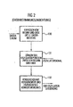
- a preferred application of the digitally controllable oscillator according to the invention is set forth in an apparatus and a method for extracting a clock frequency underlying a data stream and, in particular, for recovering this clock frequency.
- a device for extracting a clock frequency underlying a data stream wherein the data stream at regular, with a relative first accuracy specified first time intervals such.
- a first data pattern such as .z. B. has a frame start packet identification number (SOF PID)
- SOF PID frame start packet identification number
- the data stream further comprises a second A data pattern (synchronization field) having a plurality of clock periods according to the clock frequency or a multiple of the clock frequency, wherein the clock periods are specified with a second relative accuracy that is smaller than the first relative accuracy.
- the device is designed to control a controllable oscillator 10 according to the invention, i. H. to supply an oscillator controller 11 thereof with coarse tuning signals on a line 12a or fine tuning signals on a line 12b such that the oscillator controller 11 provides the controllable oscillator 10 with a corresponding voltage signal in the case of a VCO or a corresponding current signal in the controller, depending on the design of the controllable oscillator Case of an ICO can supply.
- the device comprises a coarse-tuning device 13 and a fine-tuning device 14.
- the coarse-tuning device is designed to detect a start and an end of the second data pattern (synchronization field using the example of the USB specification).
- the coarse tuning device is further configured to count a number of clock periods of the controllable oscillator 10 in a time period from the beginning to the end of the second data pattern.
- the coarse tuning means is arranged to drive the oscillator control means 11 to reduce the oscillator clock frequency of the controllable oscillator 10, or in the case where the counted number less than the reference value is to drive the controllable oscillator to increase its oscillator clock frequency.
- the fine tuning device 14 is formed. However, in contrast to the coarse-tuning device, it does not detect the beginning and the end of the second data pattern but rather the occurrence of a first data mute in FIG Data stream and a subsequent occurrence of the first data pattern in the data stream.
- the fine-tuning device is further configured to count the number of clock periods of the oscillator 10 from an occurrence of the first data pattern to a next occurrence of the first data pattern, and then to control the oscillator controller 11 according to the location of the counted value with respect to a set reference value Oscillation frequency of the controllable oscillator 10 is increased or decreased.
- an oscillator clock frequency is obtained with the relative second accuracy, that is, the accuracy underlying the first data pattern, which, depending on the specific embodiment, is immediately equal to the clock that underlies the data stream, or equal to a multiple of the clock, underlying the data stream, or equal to a fraction of the clock underlying the data stream.
- integer multiples such. For example, two times, three times, .... n times, where n is an integer.
- fractions are also integer fraction preferred, such. B. 1/2, 1/3, 1/4, ...., 1 / n, where n is also an integer.
- FIG. 1 shows a device 130 for detecting the beginning and the end of the second data pattern in the data stream, that is to say using the example of the USB data stream z.
- B the beginning of the synchronization pattern in the form of the first electrical "1” and the end of the synchronization pattern in the form of the last electrical "1" of the synchronization pattern of Fig. 7a.
- only a part of the synchronization pattern of Fig. 7a may be used as a second data pattern, so that the second data pattern using coarse tuning ticks is started with the first electrical "1" and ends with the seventh logical "0", such that only the alternating part of the synchronization pattern of Fig. 7a is used.
- only part of the alternating bit pattern could be used depending on the ratio of the frequency of the controllable oscillator to the bit clock used in FIG. 7a.
- means 131 for counting the oscillator periods between the start detected by the device 130 and the end detected by the device 130 are operated. Specifically, by a counter enable signal output by the device 130 when it detects the beginning of the second data pattern, a counter is started which counts the clock periods of the oscillator signal supplied to the device 131 until the end 130 is detected by the device 130 or according to the counter-stop signal from the device 130 to the device 131 is transmitted.
- the count may then be supplied by means 131 to means 132 configured to compare the count to a reference value and to provide a corresponding correction signal which is communicated to the oscillator controller (means 11 of FIG. 1).
- the reference value used by the device 132 depends on a nominal frequency of the oscillator 10 and a time duration or number of considered bits of the synchronization pattern shown in Fig. 7a or a part thereof. If the bit clock of the synchronization pattern in Fig. 7a z.
- the predetermined reference value will be 64. This means that in case of an optimal oscillator setting the controllable oscillator 10 would have to provide 64 clocks during the duration of the synchronization pattern of FIG. 7a. If he delivers less than 64 bars, he is too slow. If he delivers more than 64 measures, it is too fast.
- Fig. 3 shows a more detailed block diagram of the fine-tuning device 14 of Fig. 1.
- the fine-tuning device 14 of Fig. 1 comprises means 140 for detecting a first data pattern (a SOF PID using the example of the USB format) and a temporally following first data pattern.
- a counter is activated in a means 141 for counting the oscillator periods in a first data pattern, which is then stopped when a temporally following first data pattern has been detected.
- the counter in the device 141 is operative to count the clock periods of the controllable oscillator 10 of FIG.
- the count value is then applied to a means 142 which is adapted to compare this count value with a reference value and to generate the correction signal supplied to the oscillator controller 11 of FIG.
- the time interval between two consecutive first data patterns is 1 ms, as shown in FIG. 7b.
- the nominal frequency of the controllable oscillator 10 of FIG. 1 is 96 MHz again, then the predetermined reference value would be 96,000, d. H. it would take 96,000 oscillator cycles in the 1 millisecond time to set the oscillator correctly. If the count is greater than 96,000, the oscillator frequency must be reduced. If the count is less than 96,000, the oscillator frequency must be increased.
- the fine tuner shown in Fig. 3 may be further used as a frequency tracing means after both the coarse tuning and the fine tuning ends and the accuracy or the frequency tracking capability of the oscillator should be further increased, as will be explained below.
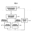
- the devices 132 of FIG. 2 or 142 of FIG. 3 are preferably designed to work iteratively, as will be explained below with reference to FIG. 4.
- the iterative approach is to first measure (40) the number of clock cycles through devices 130 and 140, respectively, to then compare the measured number to a reference value (41). If the comparison result is that the number of clock cycles is greater than the reference value, the frequency is reduced (42). If, on the other hand, it is determined that the measured number of clock cycles is less than the reference value, then the frequency of the oscillator must be increased (43). Then, an iteration variable is incremented or entered into a next step 44, in which it is now checked again whether the increased or reduced frequency in the last value is again too high or too low.
- the 1 ms frame interval is used to set the freewheeling oscillator frequency.
- the frequency accuracy of the oscillator is within the specified range of 0.25%.
- the measurement based on SYNC bits can not further improve the accuracy of the oscillator frequency. Now the fine tuning begins.
- the frequency of the oscillator after the tuning thereof is determined by the reference value FR.
- the reference value FR must be equal to 96,000 when contemplating successive SOF packets.
- the reference value is correspondingly higher.
- the reference value is correspondingly lower.
- the two-stage concept according to the invention makes it possible to achieve, on the one hand, fast and, on the other hand, accurate frequency adjustment.
- For USB applications there is only a start-up time of about 10 ms in which a new communication user must be ready. If he is not ready at this time, then there is an error signal. Due to fine-tuning only, this time is usually not enough because there are only 10 consecutive SOF PIDs in the 10 ms startup time.
- the coarse tuning z. B. carried out with the first synchronization pattern, so that in the startup time of 10 ms enough successive events remain in the data stream (eg., SOF PIDs) that a safe and accurate tuning of the now roughly tuned oscillator is achieved.
- a frequency-tracking algorithm takes place, which further sets the oscillator frequency.
- the number of oscillator periods between SOF packets present in the data stream is measured.
- the oscillator clock obtained after coarse tuning and fine tuning can be used as a reference clock for a USB core.
- Fig. 8 in which the device for extracting, designated 80, is shown.
- the extraction device therefore has, together with a controllable oscillator, the functionality of the blocks 92 and 93 of the known USB function circuit, which has been explained with reference to FIG.
- phase locking between the oscillator clock and the bit clock of the USB data stream is not required since the oscillator clock frequency is usually a multiple of the bit clock frequency and oversampling and digital PLLs can be used for data recovery.
- the device is advantageous in that for data streams, which is based on a faster clock, such. For example, for full-speed USB data streams and high-speed USB data streams, no crystal oscillator is needed. Of course, even for slower clocked data streams no external oscillators are needed.
- the device is also advantageous in that the regenerated frequency is obtained with high accuracy, which is achieved by the. Accuracy, with which the first data pattern is determined is present in the data stream.
- the example of the USB application achieves an accuracy of 0.05%.
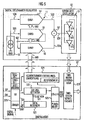
- FIG. 5 shows a clock regeneration circuit, which basically consists of two main units.
- One is the digitally controllable oscillator 50, which has an oscillator controller 11 on the one hand and the controllable oscillator 10 on the other hand, which is a current-controlled oscillator in FIG.
- FIG. 5 further shows a digital logic 52 comprising the coarse tuner 13 and the fine tuner 14, as illustrated below.
- the current-controlled oscillator 10 in the preferred embodiment shown in FIG. 5 is a current-controlled ring oscillator with an odd number of in-line inverters 51a, 51b, 51c supplied with operating current from a current summing node 52 over which an oscillation frequency of the current controlled oscillator 10 is adjustable.
- the oscillator control device 11 comprises, in addition to the current sum node 52, a supply current source or reference current source 53, which supplies a central reference (there is typically additionally a separate bias), a first digital / analog converter 54, a second digital / analog converter 55, and a
- the digital-to-analogue converters 54, 55 and 56 of FIG. 5 are designed to provide, on the output side, a current that is a fraction of the supply current supplied on the input side, wherein the selection of the fractional part over that of the Digital-to-analog converter via a digital input supplied binary number takes place.
- binary-weighted circuits. 54, 55 and 56 are preferred.
- the DAW delivers.
- the DAW 1 the value of the supply current 53 at its Output to current summation node 52 when all bits of the same supplied binary number are set. If, on the other hand, only the MSB of the DAW 1 (54) is set, while all the low-order bits are equal to 0, the DAW 1 supplies on the output side half of the current supplied by the source 53 to the current summation node. According to the invention, 9-bit DAWs are preferred, although in the embodiment also higher and lower width DAWs can be used.
- the DAW 1 54 is supplied directly by the power supply 53. It can therefore deliver the maximum amount of electricity on the output side.
- the DAW 1 is adjusted in a preferred embodiment of the present invention by the coarse tuning and the fine tuning. More specifically, the high order bits of the DAW 1 are adjusted by the coarse tuning, while the low order bits of the DAW 1 are adjusted by the fine tuning.
- the DAW 2 55 is used for frequency tracking. His supply current and thus the maximum of him to the current summation node 52 oscillator control current is controllable by the DAW 3 56.
- the output current of the DAW 3 56 is equal to the supply current 53, which leads directly to the fact that the DAW 2, if it is also supplied with all ones, can supply the same power to the summing node 52. According to the invention, however, it is preferred to apply a binary number smaller than the maximum loadable binary number to the DAW 3 in order to reduce the maximum current supplied by the DAW 2 55 to the current summing node 52.
- the DAW 2 55 can also be applied, for example, 9 bits, finely subdivided to perform a frequency tracking, to which the DAW 2 55 is used, with a finer accuracy, as determined by the LSB of the DAW 1 is determined.
- the granularity of the current output by the DAW 2 is inversely proportional to the operating current supplied to the DAW 2. The smaller the operating current supplied to the DAW 2 (set by the DAW 3), the finer the granularity in the frequency tracking mode following the fine tuning mode.
- the digitally controllable oscillator 11 thus comprises a supply source 53, the current controlled ring oscillator 10 and the three DAWs 54, 55 and 56.
- the DAWs controlled by the digital logic 52 provide the control current for frequency adjustment of the current controlled oscillator ICO 10.
- the total current for the ICO is the sum of the currents supplied by the two DAWs 54 and 55.
- the regions of the digital-to-analogue converters 1 and 2 are preferably overlapping. It is preferred that the maximum output current of the DAW 1 is a programmable multiple (programmable by the DAW 3) of the maximum output of the DAW 2. Preferably, a factor of 4 is used.
- the DAW 3 56 is biased so that the supply current in the DAC 2 is smaller by the programmable multiple than the supply current in the DAC 1. It is further preferred that during coarse tuning and fine tuning the MSB of the DAW 2 is set and / or all other bits are not set. The DAW 2 thus supplies half of the total maximum possible output current to the current summation node 52. Then, all the bits of the DAW are set by the coarse tuning mode and the fine tuning mode, thus, by additionally setting bits of the DAW 2 which have a smaller valency than the MSB thereof, the current can be increased.
- the MSB of the DAW 2 is reset and the lower order bits are set or not set as needed.
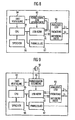
- Digital logic 52 in FIG. 5 includes the following basic functional blocks.
- the circuit comprises a synchronization field detector 520, which is also denoted by SD in FIG. 5.
- the digital logic further comprises a data recovery block 521, a frame start packet identification (SOF) PID detector 522, an oscillator clock cycle counter 523, a digital oscillator control logic 524, also designated as a correction value generator in FIG. 5, and a block 525, which is designated by clock forwarding logic and clock divider / multiplier.
- SOF frame start packet identification
- the sync field detector 520 includes an SEO detector, a sync detector, a state machine, and a dedicated counter.
- Block 520 is connected to the differential signals Dp and Dm of the USB bus.
- Block 520 is operative to listen to signals on the bus and thus monitor bus traffic to determine certain bus conditions, such as traffic conditions, using the SE0 detector. B. to detect the presence of "single-ended zero".
- both Dp and Dm are in the same state, such as Dp and Dm. B. high. Since Dp and Dm are by definition differential signals, the SE0 state is actually a forbidden state that does not contain meaningful user data. However, according to the USB specification, a state SE0 is used when the end of a package is reached.
- the SE0 detector thus detects the end of a preceding packet and thus also the beginning of a synchronization field, which the synchronization detector then detects in response to the SE0 detector.
- the state machine is activated in block 520 to await receipt of a synchronization pattern as shown in FIG. 7a.
- the counter in block 520 measures the length of the synchronization pattern by counting the number of oscillator periods between the beginning and the end of the synchronization field.
- the data recovery block 521 is enabled or enabled by the block 520 via the line labeled EN after the block 520 has received a valid synchronization pattern.
- the data recovery unit 521 is deactivated again when the block 520 has received a state SE0.
- the measurement result from block 520 in terms of the length of the synchronization field is supplied to block 521, which uses this information to extract "zeros" and "ones" from the USB serial data stream, that is, to decode the data stream Recover information contained in the data stream.
- the frame start packet identification detector 521 also referred to as the SOF token detector, examines the serial data stream from the block 521 and signals the counter 523 when it has detected a frame start packet identification number (SOF-PID).
- SOF-PID frame start packet identification number
- the oscillator clock cycle counter 523 counts the number of DCO periods between the receipt of consecutive SOF tokens.
- the counter 523 includes a plausibility checker that examines whether SOF tokens have been missed.
- the plausibility checker is configured to compare a coarse count value with a current count value. If the current count exceeds the coarse count by a very large amount, this indicates that at least one SOF PID has been missed between two sensed SOF PIDs. In this case, the counter 523 is controlled so that this count value is not provided to the device 524, as this would result in a large misadjustment of the controllable oscillator. Instead, this count is marked as implausible and discarded.
- the correction value generation means 524 performs frequency tuning and frequency tracking. After a reset, the frequency tuning algorithm is active. First, the frequency of the oscillator is coarsely tuned. For coarse tuning, the cycle number of the synchronization pattern measured by block 520 is used. The coarse tuning determines the most significant bits of the DAW 1 as it has been executed. With each tuning step, the low order bits are gradually determined. After a certain number of coarse tuning steps, where three steps are preferred for coarse tuning at a bit width of the DAW 1 of 9, the fine tuning algorithm starts activated by a controller shown in Fig. 1 which principally controls the steps of coarse tuning, fine tuning and frequency tracking.
- the number of fine tuning steps is D1 - C.
- the frequency tracking takes place after the fine tuning.
- the cycle count of counter 521 is also used in frequency tracking to further tune the oscillator frequency across the DAW 55.
- FIG. 6 illustrates the functionality of the correction value generator 524 in more detail.
- a first step 60 the most significant bit of the DAW 1 is set equal to 1, while the remaining bits are set to 0.
- the MSB of the DAW 2 is also set throughout the coarse and fine tuning, while the remaining bits of the DAW 2 are 0.
- the means 524 performs a frequency comparison based on the input values of the coarse tuning block SD 520 or the fine tuning counter 523. If the frequency is too large, the MSB of the DAW 1 is set equal to 0. On the other hand, if the frequency is too small, the MSB of the DAW 1 remains at 1. Then, the device 524 operates to set the MSB-1 of the DAW 1 in step 62 after the MSB is as in step 61 has been determined.
- step 63 means 524 is again operative to perform a frequency comparison. If the frequency is too high, the bit MSB-1 of the DAW 1 is reset to 0. If, on the other hand, the frequency is too low, then the bit MSB-1 of the DAW 1 remains at its set value, i. H. 1. In this manner, the successive iterative approximation is advanced until a corresponding predetermined number of bits of the DAW 1 are set. Then, by the controller 15 of FIG. 1, the correction value generator 524 is activated to go from the coarse tuning mode to the fine tuning mode and no longer to operate based on the counts of the block 520 but based on the counts of the block 523 to tune in fine tuning mode to calculate the remaining bits of the DAW 1 bit by bit.
- the frequency tracking mode (65) is switched, in which the bits of the DAW 2 are adjusted accordingly. If 64 of the fine-tuning mode is detected in the last step, that the frequency was too small, this indicates that the MSB of the DAW 2 initially set to 1 in step 60 is rightly 1. If, on the other hand, in the last step 64 of the fine-tuning mode it is found that the frequency is too high, the MSB of the DAW 2 is set to 0 and the successive approximation to the MSB -1 of the DAW. 2 carried out gradually.
- the DAW 3 can be reprogrammed at certain points in time in order to set the maximum output current and thus the granularity of the DAW 2 or to adapt it to changing circumstances.
Landscapes
- Stabilization Of Oscillater, Synchronisation, Frequency Synthesizers (AREA)
- Synchronisation In Digital Transmission Systems (AREA)
Claims (12)
- Oscillateur à commande numérique ayant les caractéristiques suivantes :un dispositif (10) de génération d'oscillations, qui est formé pour générer une oscillation, qui a une fréquence, qui peut être réglée dans le dispositif (10) de génération d'oscillations par l'intermédiaire d'un signal (501) d'entrée analogique ; etune commande (11) de l'oscillateur pour générer le signal (501) d'entrée analogique, la commande de l'oscillateur présentant les caractéristiques suivantes :caractérisé en ce queun premier convertisseur (54) numérique/analogique pour fournir un premier signal (502) de sortie du convertisseur numérique/analogique en réponse à un premier signal (503) d'entrée numérique ;un deuxième convertisseur (55) numérique/analogique pour fournir un deuxième signal de sortie du convertisseur numérique/analogique en réponse à un deuxième signal (505) d'entrée numérique ; etun combinateur (52) pour combiner le premier et le deuxième signal (502, 504) de sortie du convertisseur numérique/analogique, afin d'obtenir le signal (501) d'entrée analogique pour le dispositif (10) de génération d'oscillations,le deuxième convertisseur (55) numérique/analogique étant formé, pour fournir une différence dans le deuxième signal (504) de sortie du convertisseur numérique/analogique en réponse à un incrément numérique dans le deuxième signal (505) d'entrée numérique, qui est inférieure à une différence dans le premier signal (502) de sortie du convertisseur numérique/analogique, lorsque le premier convertisseur (54) numérique/analogique ayant l'incrément numérique est injecté dans le premier signal (503) d'entrée numérique,le premier convertisseur (54) numérique/analogique et/ou le deuxième convertisseur (55) numérique/analogique étant formés pour fournir une différence dans le premier ou dans le deuxième signal de sortie en réponse à un incrément numérique, signal de sortie qui dépend d'une grandeur d'alimentation pour le convertisseur numérique/analogique,la grandeur d'alimentation pour le deuxième convertisseur (55) numérique/analogique se différenciant d'une grandeur d'alimentation pour le premier convertisseur (54) numérique/analogique,
la commande de l'oscillateur présente un troisième convertisseur (56) numérique/analogique, qui est câblé avec le deuxième convertisseur numérique/analogique de telle sorte qu'il fournisse la grandeur (507) d'alimentation pour le deuxième convertisseur numérique/analogique, la grandeur (507) d'alimentation pour le deuxième convertisseur numérique/analogique pouvant être réglée dans le troisième convertisseur numérique/analogique par l'intermédiaire d'un signal (508) d'entrée numérique. - Oscillateur à commande numérique suivant la revendication 1, pour lequel le premier convertisseur (54) numérique/analogique et/ou le deuxième convertisseur (55) nuémrique/analogique sont formés pour fournir une différence dans le premier ou dans le deuxième signal de sortie en réponse à un incrément numérique, signal de sortie qui dépend d'une grandeur (506, 507) d'alimentation pour le convertisseur numérique/analogique.
- Oscillateur à commande numérique suivant la revendication 1, pour lequel la commande (11) de l'oscillateur présente en outre la caractéristique suivante :une source (53) d'alimentation pour fournir une grandeur (506) d'alimentation, etpour lequel le premier et le troisième convertisseur (54, 56) numérique/analogique sont alimentés par la source d'alimentation ayant la même grandeur (506) d'alimentation, etpour lequel le deuxième convertisseur (55) numérique/analogique est alimenté par une grandeur (507) d'alimentation, qui est inférieure à la grandeur (506) d'alimentation pour le premier et le troisième convertisseur numérique/analogique, la grandeur d'alimentation pour le deuxième convertisseur numérique/analogique pouvant être réglée par le signal (508) d'entrée numérique dans le troisième convertisseur numérique/analogique.
- Oscillateur à commande numérique suivant la revendication 1 ou 3, pour lequel le premier, le deuxième et le troisième convertisseur numérique/analogique sont formés de façon identique.
- Oscillateur à commande numérique suivant la revendication 1 ou 3, pour lequel le premier, le deuxième et le troisième convertisseur numérique/analogique sont intégrés dans un circuit.
- Oscillateur à commande numérique suivant l'une des revendications précédentes,
pour lequel le dispositif (10) de génération d'oscillations présente un nombre impair d'inverseurs (51a, 51b, 51c), qui sont montés sur un anneau, les inverseurs pouvant être alimentés par le signal (501) d'entrée analogique. - Oscillateur à commande numérique suivant l'une des revendications précédentes, pour lequel le premier et le troisième signal de sortie du convertisseur numérique/analogique et le signal d'entrée analogique sont un courant.
- Oscillateur à commande numérique suivant l'une des revendications précédentes, pour lequel l'incrément numérique comprend une modification d'un mot binaire, qui peuvent être livrés au premier et au deuxième convertisseur numérique/analogique en tant que signaux (503, 505) d'entrée, d'un bit.
- Oscillateur à commande numérique suivant l'une des revendications précédentes,
pour lequel le premier convertisseur numérique/analogique peut être amorcé dans un mode d'accord, et pour lequel le deuxième convertisseur numérique/analogique peut être amorcé dans un mode de poursuite en fréquence,
le premier convertisseur numérique/analogique ayant un signal (503) d'entrée numérique constant pouvant être injecté dans le mode de poursuite en fréquence, et
le deuxième convertisseur numérique/analogique ayant un deuxième signal (505) d'entrée numérique constant pouvant être injecté dans le mode d'accord. - Oscillateur à commande numérique suivant la revendication 9, pour lequel le deuxième signal (505) d'entrée numérique dans le deuxième convertisseur numérique/analogique dans le mode d'accord est choisi de telle sorte qu'à la fin du mode d'accord le signal (501) d'entrée analogique peut être modifié dans le dispositif (10) de génération d'oscillations pour obtenir des valeurs plus grandes et plus petites en modifiant le signal d'entrée numérique dans le deuxième convertisseur numérique/analogique dans le mode de poursuite en fréquence.
- Oscillateur à commande numérique suivant la revendication 9 ou 10,
pour lequel le deuxième convertisseur numérique/analogique est injecté avec un signal d'entrée numérique dans le mode d'accord, dans lequel le premier convertisseur numérique/analogique peut être amorcé de façon grandeur, dans lequel un bit de la plus grande valeur possible est mis et tous les bits de moindre valeur ne sont pas mis de telle sorte que le deuxième signal (504) de sortie du convertisseur numérique/analogique a une grandeur, qui est à peu près égale à la moitié d'une grandeur du signal de sortie, qui peut être atteint au maximum, du deuxième convertisseur (55) numérique/analogique. - Oscillateur à commande numérique suivant l'une des revendications précédentes, pour lequel le premier (54) et/ou le deuxième (55) convertisseur numérique/analogique peuvent être injectés du côté de l'entrée avec un nombre binaire d'une largeur de n bits,
le premier et/ou le deuxième convertisseur numérique/analogique pouvant être alimenté par une grandeur (53) d'entrée électrique,
une grandeur de commande fournie du côté de la sortie par le convertisseur numérique/analogique pouvant être livrée au combinateur, et
une somme de la grandeur de commande électrique étant égale à un rapport, qui est fixé par le nombre binaire et la grandeur d'entrée électrique.
Applications Claiming Priority (3)
| Application Number | Priority Date | Filing Date | Title |
|---|---|---|---|
| DE10260713 | 2002-12-23 | ||
| DE10260713A DE10260713B4 (de) | 2002-12-23 | 2002-12-23 | Digital steuerbarer Oszillator |
| PCT/EP2003/014816 WO2004059847A1 (fr) | 2002-12-23 | 2003-12-23 | Oscillateur a commande numerique |
Publications (2)
| Publication Number | Publication Date |
|---|---|
| EP1573921A1 EP1573921A1 (fr) | 2005-09-14 |
| EP1573921B1 true EP1573921B1 (fr) | 2006-04-05 |
Family
ID=32519330
Family Applications (1)
| Application Number | Title | Priority Date | Filing Date |
|---|---|---|---|
| EP03785928A Expired - Lifetime EP1573921B1 (fr) | 2002-12-23 | 2003-12-23 | Oscillateur a commande numerique |
Country Status (5)
| Country | Link |
|---|---|
| US (1) | US7081583B2 (fr) |
| EP (1) | EP1573921B1 (fr) |
| AU (1) | AU2003294945A1 (fr) |
| DE (2) | DE10260713B4 (fr) |
| WO (1) | WO2004059847A1 (fr) |
Families Citing this family (9)
| Publication number | Priority date | Publication date | Assignee | Title |
|---|---|---|---|---|
| DE60334866D1 (de) * | 2002-07-17 | 2010-12-16 | Chronologic Pty Ltd | Synchronisierter Multikanal-USB |
| TW200427225A (en) * | 2003-05-23 | 2004-12-01 | Genesys Logic Inc | Method of auto-tracking and compensating clock frequency and related apparatus thereof |
| JP4434906B2 (ja) * | 2004-10-01 | 2010-03-17 | 三洋電機株式会社 | 発振周波数制御回路 |
| TWI429199B (zh) * | 2010-06-22 | 2014-03-01 | Phison Electronics Corp | 產生參考時脈訊號的方法及資料收發系統 |
| TWI420802B (zh) * | 2010-06-30 | 2013-12-21 | Weltrend Semiconductor Inc | 自動校正頻率之頻率校正電路及其方法 |
| TWI545419B (zh) * | 2015-05-08 | 2016-08-11 | 偉詮電子股份有限公司 | 自動校正非晶體振盪器之時脈之裝置及其方法 |
| JP6703814B2 (ja) * | 2015-08-28 | 2020-06-03 | ルネサスエレクトロニクス株式会社 | Ad変換器及びad変換装置 |
| US9912320B2 (en) | 2016-06-13 | 2018-03-06 | The Hong Kong University Of Science And Technology | Exponentially scaling switched capacitor |
| TWI629597B (zh) * | 2017-03-14 | 2018-07-11 | 芯籟半導體股份有限公司 | 一種時脈訊號處理系統及其方法 |
Family Cites Families (6)
| Publication number | Priority date | Publication date | Assignee | Title |
|---|---|---|---|---|
| US4568888A (en) * | 1983-11-08 | 1986-02-04 | Trw Inc. | PLL Fast frequency synthesizer with memories for coarse tuning and loop gain correction |
| US4929918A (en) * | 1989-06-07 | 1990-05-29 | International Business Machines Corporation | Setting and dynamically adjusting VCO free-running frequency at system level |
| JPH1056329A (ja) * | 1996-08-12 | 1998-02-24 | Matsushita Electric Ind Co Ltd | 周波数制御発振器 |
| US6411237B1 (en) * | 1997-10-21 | 2002-06-25 | Emhiser Research Ltd | Nonlinear digital-to-analog converters |
| EP1216471B1 (fr) * | 1999-07-07 | 2015-05-20 | Gibson Brands, Inc. | Dispositif d'enregistrement numerique d'instruments de musique interactif |
| US6989484B2 (en) * | 2001-04-17 | 2006-01-24 | Intel Corporation | Controlling sharing of files by portable devices |
-
2002
- 2002-12-23 DE DE10260713A patent/DE10260713B4/de not_active Expired - Fee Related
-
2003
- 2003-12-23 AU AU2003294945A patent/AU2003294945A1/en not_active Abandoned
- 2003-12-23 WO PCT/EP2003/014816 patent/WO2004059847A1/fr not_active Ceased
- 2003-12-23 DE DE50302923T patent/DE50302923D1/de not_active Expired - Lifetime
- 2003-12-23 EP EP03785928A patent/EP1573921B1/fr not_active Expired - Lifetime
-
2005
- 2005-06-23 US US11/166,685 patent/US7081583B2/en not_active Expired - Lifetime
Also Published As
| Publication number | Publication date |
|---|---|
| DE50302923D1 (de) | 2006-05-18 |
| US20060021491A1 (en) | 2006-02-02 |
| US7081583B2 (en) | 2006-07-25 |
| WO2004059847A1 (fr) | 2004-07-15 |
| DE10260713B4 (de) | 2005-05-04 |
| AU2003294945A1 (en) | 2004-07-22 |
| EP1573921A1 (fr) | 2005-09-14 |
| DE10260713A1 (de) | 2004-07-22 |
Similar Documents
| Publication | Publication Date | Title |
|---|---|---|
| EP1576761B1 (fr) | Procede et dispositif pour extraire une frequence d'horloge a la base d'un flux de donnees | |
| DE69613660T2 (de) | Energiesparende Phasenregelkreisschaltung | |
| DE19703986C2 (de) | Signalformereinrichtung und Taktsignalzuführvorrichtung | |
| DE3785966T2 (de) | Digitale, phasenverriegelte Taktwiedergewinnungsschleife. | |
| DE69926320T2 (de) | Durch digitale wörter abgestimmte frequenzsyntheseschaltung | |
| DE68915756T2 (de) | Programmierbarer hochgeschwindigkeitsteiler. | |
| DE3841512C2 (fr) | ||
| DE3587141T2 (de) | Zentrierschaltung eines spannungsgesteuerten oszillators. | |
| DE10123973A1 (de) | Jitter-reduzierte PLL-Schaltung mit einer mehrstufigen digitalen Verzögerungsleitung | |
| DE10041772A1 (de) | Taktgenerator, insbesondere für USB-Geräte | |
| DE69332698T2 (de) | Verfahren und vorrichtung zur erzeugung eines protokolls für eine digitale audioschnittstelle | |
| EP1573921B1 (fr) | Oscillateur a commande numerique | |
| DE69500892T2 (de) | PLL-Synthetisierer | |
| DE69411511T2 (de) | Schaltung zur Taktrückgewinnung mit angepassten Oszillatoren | |
| EP1198889B1 (fr) | Generateur de signal d'horloge | |
| DE102023107496A1 (de) | Unabhängiges takten eines digitalen schleifenfilters durch zeit-digital-wandler in digitaler phasenregelschleife | |
| DE10234993B4 (de) | Akkumulator gesteuerter digitaler Frequenzteiler in einer phasenverriegelten Schleife | |
| DE69803625T2 (de) | Frequenzteilungsvorrichtung, bestehend aus einem Vorzähler gefolgt von einem programmierbaren Zähler und Anwendung in einem Frequenzsynthetisierer | |
| DE102023106902A1 (de) | Sigma-delta-modulator für die hochauflösende steuerung eines ringoszillators in einer digitalen phasenregelschleife | |
| EP1010236B1 (fr) | Circuit oscillateur a quartz piezoelectrique | |
| EP1050126B1 (fr) | Circuit a commande numerique pour reduire la modulation de phase d'un signal | |
| DE3906094A1 (de) | Digitale phasen/frequenz-detektorschaltung | |
| DE69002224T2 (de) | Mikrowellen-Synthesierer mit einem Teiler mit gebrochenem Teilverhältnis. | |
| DE102006050881B3 (de) | Phasen-/Frequenzvergleicher, Phasenregelkreis, Verfahren zur Phasen-/Frequenzdetektion und Verfahren zum Erzeugen eines Oszillatorsignals | |
| EP1646150B1 (fr) | Procédé et dispositif pour extraire une fréquence d'horloge à la base d'un flux de données |
Legal Events
| Date | Code | Title | Description |
|---|---|---|---|
| PUAI | Public reference made under article 153(3) epc to a published international application that has entered the european phase |
Free format text: ORIGINAL CODE: 0009012 |
|
| 17P | Request for examination filed |
Effective date: 20050429 |
|
| AK | Designated contracting states |
Kind code of ref document: A1 Designated state(s): AT BE BG CH CY CZ DE DK EE ES FI FR GB GR HU IE IT LI LU MC NL PT RO SE SI SK TR |
|
| AX | Request for extension of the european patent |
Extension state: AL LT LV MK |
|
| GRAP | Despatch of communication of intention to grant a patent |
Free format text: ORIGINAL CODE: EPIDOSNIGR1 |
|
| GRAS | Grant fee paid |
Free format text: ORIGINAL CODE: EPIDOSNIGR3 |
|
| GRAA | (expected) grant |
Free format text: ORIGINAL CODE: 0009210 |
|
| AK | Designated contracting states |
Kind code of ref document: B1 Designated state(s): DE FR |
|
| DAX | Request for extension of the european patent (deleted) | ||
| RBV | Designated contracting states (corrected) |
Designated state(s): DE FR |
|
| REF | Corresponds to: |
Ref document number: 50302923 Country of ref document: DE Date of ref document: 20060518 Kind code of ref document: P |
|
| ET | Fr: translation filed | ||
| PLBE | No opposition filed within time limit |
Free format text: ORIGINAL CODE: 0009261 |
|
| STAA | Information on the status of an ep patent application or granted ep patent |
Free format text: STATUS: NO OPPOSITION FILED WITHIN TIME LIMIT |
|
| 26N | No opposition filed |
Effective date: 20070108 |
|
| REG | Reference to a national code |
Ref country code: FR Ref legal event code: PLFP Year of fee payment: 13 |
|
| REG | Reference to a national code |
Ref country code: FR Ref legal event code: PLFP Year of fee payment: 14 |
|
| REG | Reference to a national code |
Ref country code: FR Ref legal event code: PLFP Year of fee payment: 15 |
|
| PGFP | Annual fee paid to national office [announced via postgrant information from national office to epo] |
Ref country code: FR Payment date: 20191219 Year of fee payment: 17 |
|
| PG25 | Lapsed in a contracting state [announced via postgrant information from national office to epo] |
Ref country code: FR Free format text: LAPSE BECAUSE OF NON-PAYMENT OF DUE FEES Effective date: 20201231 |
|
| PGFP | Annual fee paid to national office [announced via postgrant information from national office to epo] |
Ref country code: DE Payment date: 20220225 Year of fee payment: 19 |
|
| REG | Reference to a national code |
Ref country code: DE Ref legal event code: R119 Ref document number: 50302923 Country of ref document: DE |
|
| PG25 | Lapsed in a contracting state [announced via postgrant information from national office to epo] |
Ref country code: DE Free format text: LAPSE BECAUSE OF NON-PAYMENT OF DUE FEES Effective date: 20230701 |