EP1575202A1 - Ofdm-sende-/-empfangsvorrichtung - Google Patents
Ofdm-sende-/-empfangsvorrichtung Download PDFInfo
- Publication number
- EP1575202A1 EP1575202A1 EP02786143A EP02786143A EP1575202A1 EP 1575202 A1 EP1575202 A1 EP 1575202A1 EP 02786143 A EP02786143 A EP 02786143A EP 02786143 A EP02786143 A EP 02786143A EP 1575202 A1 EP1575202 A1 EP 1575202A1
- Authority
- EP
- European Patent Office
- Prior art keywords
- signal
- ofdm
- carrier
- cross
- carrier wave
- Prior art date
- Legal status (The legal status is an assumption and is not a legal conclusion. Google has not performed a legal analysis and makes no representation as to the accuracy of the status listed.)
- Granted
Links
Images


Classifications
-
- H—ELECTRICITY
- H04—ELECTRIC COMMUNICATION TECHNIQUE
- H04L—TRANSMISSION OF DIGITAL INFORMATION, e.g. TELEGRAPHIC COMMUNICATION
- H04L5/00—Arrangements affording multiple use of the transmission path
- H04L5/02—Channels characterised by the type of signal
- H04L5/04—Channels characterised by the type of signal the signals being represented by different amplitudes or polarities, e.g. quadriplex
-
- H—ELECTRICITY
- H04—ELECTRIC COMMUNICATION TECHNIQUE
- H04B—TRANSMISSION
- H04B7/00—Radio transmission systems, i.e. using radiation field
- H04B7/02—Diversity systems; Multi-antenna system, i.e. transmission or reception using multiple antennas
- H04B7/10—Polarisation diversity; Directional diversity
-
- H—ELECTRICITY
- H04—ELECTRIC COMMUNICATION TECHNIQUE
- H04L—TRANSMISSION OF DIGITAL INFORMATION, e.g. TELEGRAPHIC COMMUNICATION
- H04L27/00—Modulated-carrier systems
- H04L27/26—Systems using multi-frequency codes
- H04L27/2601—Multicarrier modulation systems
- H04L27/2626—Arrangements specific to the transmitter only
- H04L27/2627—Modulators
-
- H—ELECTRICITY
- H04—ELECTRIC COMMUNICATION TECHNIQUE
- H04L—TRANSMISSION OF DIGITAL INFORMATION, e.g. TELEGRAPHIC COMMUNICATION
- H04L27/00—Modulated-carrier systems
- H04L27/26—Systems using multi-frequency codes
- H04L27/2601—Multicarrier modulation systems
- H04L27/2647—Arrangements specific to the receiver only
- H04L27/2649—Demodulators
Definitions
- This invention relates to an Orthogonal Frequency Division Multiplex (OFDM) transceiver apparatus and, more particularly, to an OFDM transmitter apparatus and OFDM receiver apparatus for performing OFDM communication utilizing a plurality of polarized waves.
- OFDM Orthogonal Frequency Division Multiplex
- OFDM Orthogonal Frequency Division Multiplex
- FIG. 9 (a) is a schematic structural view of a multicarrier transmission scheme.
- a serial/parallel converter 1 converts serial data to parallel data and inputs the parallel data to quadrature modulators 3a to 3d via low-pass filters 2a to 2d, respectively.
- the conversion is to parallel data comprising four symbols S1 to S4. Each symbol includes an in-phase component and a quadrature component.
- the quadrature modulators 3a to 3d subject each of the symbols to quadrature modulation by carriers having frequencies f 1 to f 4 illustrated in (b) of Fig.
- a combiner 4 combines the quadrature-modulated signals and a transmitter (not shown) up-converts the combined signal to a high-frequency signal and then transmits the high-frequency signal.
- the frequencies are arranged, as shown at (b) of Fig. 9, in such a manner that the spectrums will not overlap in order to satisfy the orthogonality of the carriers.
- Fig. 10(a) is a diagram of the structure of a transmitting apparatus that relies upon the OFDM transmission scheme.
- a serial/parallel converter 5 converts serial data to parallel data comprising M-number of symbols.
- An IFFT (Inverse Fast Fourier Transform) 6 which is for the purpose of transmitting the M-number of symbols as carriers having a frequency spacing shown at (b) of Fig. 10, applies an inverse discrete Fourier transform to the frequency data to effect a conversion to time data.
- a guard interval inserting unit 7 inserts a guard interval GI and inputs real and imaginary parts to a quadrature modulator 9 through low-pass filters 8a, 8b.
- the quadrature modulator 9 subjects the input data to quadrature modulation, and a transmitter (not shown) up-converts the modulated signal to a high-frequency signal.
- a frequency placement of the kind shown at (b) of Fig. 10 becomes possible, thereby enabling an improvement in the efficiency with which frequency is utilized.
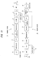
- Fig. 11 is a diagram showing the conventional structure of an Orthogonal Frequency Division Multiplex (OFDM) communication apparatus, in which TR and RV represent transmit and receive channels.
- a serial/parallel (S/P) converter 10 converts transmit data, which enters in a serial format, to M-bit parallel data
- a mapping unit 11 maps the M-bit parallel data to N-number of carriers based upon a modulation scheme of each carrier. For example, if it is assumed that QPSK modulation is performed by all carriers, the M-bit parallel data is divided into N-sets of two bits each and the 2-bit data of the N sets obtained by division is mapped to each carrier.
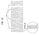
- Fig. 12 is a diagram useful in describing carrier placement. Here carriers for transmitting a pilot have been inserted.
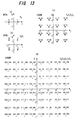
- Fig. 13 is a diagram of signal-point placement for describing mapping.
- (a) is a case where BPSK modulation is performed, and one bit (b 0 ) at a time is mapped to a carrier;
- (b) is a case where QPSK modulation is performed, and two bits (b 0 b 1 ) at a time are mapped to a carrier;
- (c) is a case where 16QAM modulation is performed, and four bits (b 0 b 1 b 2 b 3 ) at a time are mapped to a carrier; and
- (d) is a case where 64QAM modulation is performed, and six bits (b 0 b 1 b 2 b 3 b 4 b 5 ) at a time are mapped to a carrier.
- an IFFT arithmetic unit 12 applies IFFT processing to the symbol data of N carriers to convert the data to two time waveform signals (PCM waveform signals) of a real number (Ich component) and imaginary number (Qch component).
- a guard interval inserting unit 13 inserts a GI (Guard Interval) into each signal, and a waveshaping unit 14 shapes the waveforms and inputs the results to an IQ modulator (QPSK quadrature modulator) 15.
- QPSK quadrature modulator quadrature modulator
- the latter applies quadrature modulation to the Ich signal and Qch signal input thereto, and a mixer 16 multiplies the modulated signal of the baseband by a high-frequency carrier wave that enters from a carrier wave generator 17, thereby performing a frequency conversion.
- a transmit amplifier 18 amplifies the transmit signal and transmits the amplified signal from an antenna ATT.
- a high-frequency amplifier 20 of a radio unit amplifies a receive signal from an antenna ATR, and a mixer 21 multiplies the receive signal by a high-frequency carrier wave that enters from a carrier wave generator 22, thereby effecting a frequency conversion to a baseband signal, and inputs the signal to an IQ demodulator (QPSK quadrature demodulator) 23.
- the latter subjects the input signal to quadrature demodulation to demodulate and output the Ich signal and Qch signal.
- a waveshaping unit 24 shapes each of the waveforms and inputs the results to a rotator 25. The latter detects phase-error information from a known pilot signal and rotates phase in such a manner that the phase error becomes zero.
- a GI removing unit 26 removes the GI (Guard Interval) from the input signal of each component, and an FFT arithmetic unit 27 applies FFT processing to the time waveform signals input thereto and outputs N-number of carrier components.
- a demapping unit 28 performs demapping (processing that is the reverse of mapping) on a per-carrier basis and outputs M-bit parallel data, and a parallel/serial (P/S) converter 29 converts the M-bit parallel data to serial data and outputs the serial data.
- P/S parallel/serial
- a wired LAN generally is implemented according to 100Base-TX (100 Mbps), and a wireless LAN system having a communication speed equivalent to this is required.
- Methods of enlarging transmission capacity without changing the frequency band include a co-channel transmission method.
- polarization horizontal polarization and vertical polarization
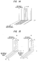
- transmission speed is doubled overall, as illustrated in Fig. 14.
- two OFDM transceivers are required.
- Cross-polarization interference occurs owing to a shift in antenna polarization angle.
- cross-polarization interference occurs also owing to distortion in the transmission path conforming to rainfall and other factors. This makes it necessary to construct an OFDM transceiver in such a manner that such cross-polarization interference can be eliminated.
- an object of the present invention is to so arrange it that a phase deviation between polarized waves will not occur.
- Another object of the present invention is to simply the structure of a canceller for eliminating cross-polarization interference.
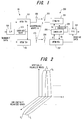
- a first aspect of the present invention is an OFDM transmitter apparatus for transmitting signals, which are output from first and second OFDM transmit circuits, utilizing two mutually orthogonal polarized waves.
- a single carrier wave generator is provided in common for the OFDM transmit circuits, and a frequency converter in each OFDM transmit circuit multiplies a baseband signal by a carrier wave, which is output from the carrier wave generator, to convert the baseband signal to a radio signal.
- a phase deviation will not occur between a vertically polarized wave and a horizontally polarized wave by adopting a common transmit carrier wave in the first and second OFDM transmit circuits.
- a second aspect of the present invention is an OFDM receiver apparatus having first and second OFDM receive circuits for demodulating respective ones of signals that have been transmitted utilizing two mutually orthogonal polarized waves.
- the OFDM receiver apparatus is such that a carrier wave generator is provided in common for the OFDM receive circuits, and a frequency converter in each OFDM receive circuit multiplies a radio signal by a carrier wave, which is output from the carrier wave generator, to convert the radio signal to a baseband signal, and inputs the baseband signal to a demodulator.
- the OFDM receive circuits includes a demodulator for performing demodulation onto the baseband signal; an FFT arithmetic unit for applying FFT processing to a demodulated signal; an error signal generator for generating an error signal based upon each carrier signal obtained by the FFT processing; and a cross-polarization interference canceller for correcting an output signal of the demodulator by generating a cross-polarization interference compensating signal using the error signal and a demodulated signal from the other OFDM receive circuit.
- Cross-polarization interference caused by a shift in antenna polarization angle or distortion in the transmission path conforming to rainfall and other factors can be eliminated by the cross-polarization interference canceller.
- the other OFDM receive circuit includes a demodulator for performing demodulation on to the baseband signal; an FFT arithmetic unit for applying FFT processing to a demodulated signal; an error signal generator for generating an error signal based upon each carrier signal obtained by the FFT processing; and a cross-polarization interference canceller for correcting each carrier signal of the FFT by generating a cross-polarization interference compensating signal using the error signal and a demodulated signal from the other OFDM receive circuit.
- the speed per symbol of each carrier becomes 1/N, where N represents the number of carriers in the OFDM transmission, the amount of delay of interference waves becomes relatively small, the number of taps of a FIR constituting the canceller can be reduced and the scale of the circuitry can be reduced overall.
- a frequency converter (not shown) in each of the OFDM transmit circuits 101, 102 multiplies the carrier wave that is output from the carrier wave generator 103 by a baseband signal, thereby effecting a conversion to a radio signal.
- the OFDM transmit circuit 101 transmits the radio signal from an antenna 105 by vertically polarized waves
- the OFDM transmit circuit 102 transmits the radio signal from an antenna 106 by horizontally polarized waves.
- An OFDM receiver apparatus 200 includes first and second OFDM receive circuits 201, 202 for receiving signals, which have been transmitted utilizing two mutually orthogonal polarized waves, by antennas 203, 204, respectively, and for demodulating respective ones of these signals.
- the OFDM receive circuits 201, 202 are each provided with cross-polarization interference cancellers 205, 206.
- the cross-polarization interference cancellers 205, 206 share a transmit carrier wave or a receive carrier wave between polarized waves, thereby making it possible to extract and cancel a cross-polarization interference component.
- the cross-polarization interference canceller 205 generates a cross-polarization interference compensating signal AC using the demodulated signal from the second OFDM receive circuit 202, and the first OFDM receive circuit 201 corrects the output signal of the demodulator using the cross-polarization interference compensating signal AC.
- the cross-polarization interference canceller 206 generates a cross-polarization interference compensating signal BC using the demodulated signal from the first OFDM receive circuit 201, and the second OFDM receive circuit 202 corrects the output signal of the demodulator using the cross-polarization interference compensating signal BC.
- a parallel/serial converter 207 combines the parallel data that is output from the first and second OFDM receive circuits 201, 202, effects a conversion to serial data and outputs the serial data.
- Orthogonality of adjacent carriers in OFDM is a well-known fact if the principle of a fast inverse discrete Fourier transform is utilized.
- Carrier C A and carrier C B in Fig. 2 are always in an orthogonal relationship and do not produce interference. Further, carrier C A and carrier C D give rise to interference between polarized waves, but in a case where a common transmit carrier wave was not used between the polarized waves, interference equivalent to the difference between the frequencies of the transmit carrier waves is produced between carrier C A and carrier C E as well. In order to prevent this, a common transmit carrier wave is adopted, thereby making it possible to maintain the orthogonality between carrier C A and carrier C E .
- cross-polarization interference between carrier C A and carrier C D is cancelled by the OFDM receive circuits 201, 202 by generating the cross-polarization interference compensating signals in the cross-polarization interference cancellers 205, 206, thereby making it possible to eliminate interference between cross-polarized waves.
- the cross-polarization interference compensating signal is generated by the canceller 205 and interference between differently polarized waves can be eliminated.
- Fig. 3 is a diagram of the structure of an OFDM transmitter apparatus according to the present invention. Here components identical with those of in Fig. 1 are designated by like reference characters.
- the first and second OFDM transmit circuits 101, 102 transmit a transmit signal by an orthogonal polarization scheme, i.e., upon dividing the signal into two polarized waves (e.g., waves that differ by an angle of 90°).
- the serial/parallel (S/P) converter 104 converts the transmit data, which enters in a serial format, to M-bit parallel data, inputs half the parallel data to the first OFDM transmit circuit 101 and inputs the other half to the OFDM transmit circuit 102.
- Mapping units 111a, 111b map the M/2-bit parallel data to N-number of carriers based upon the carrier modulation method. For example, if QPSK modulation is performed by all carriers, then M/2-bit parallel data is divided into N sets of two bits each and the N sets of 2-bit data obtained by division are mapped to each carrier. In actuality, the mapping units 111a, 111b perform mapping based upon 4QAM - 64QAM modulation schemes on the basis of the S/N ratio of each carrier.
- IFFT arithmetic units 112a, 112b apply IFFT processing to the symbol data of the N carriers and effect a conversion to two time waveform signals (PCM waveform signals) of a real number (Ich component) and imaginary number (Qch) component.
- Guard interval inserting units 113a, 113b insert a GI (Guard Interval) into each signal, and waveshaping units 114a, 114b shape the waveforms and input the results to IQ modulators (QPSK quadrature modulators) 115a, 115b.
- GI Guard Interval
- mixers 116a, 116b multiply the modulated signals of the baseband that are output from the quadrature modulators 115a, 115b by a high-frequency carrier wave that enters from the carrier wave generator 103, thereby performing a frequency conversion.
- Transmit amplifiers 117a, 117b amplify the transmit signals and transmit the amplified signals from antennas 105, 106 in such a manner that the polarization planes of the carrier waves are rendered mutually orthogonal.
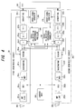
- Fig. 4 is a diagram of the structure of an OFDM receiver apparatus according to the present invention. Components identical with those shown in Fig. 1 are designated by like reference characters.
- LNA (low-noise amplifier) units 201a, 202a of the first and second OFDM receive circuits 201, 202 amplify receive signals from two antennas 203, 204 having different polarizations, and mixers 201b, 202b multiply the receive signals by a high-frequency carrier wave that enters from a carrier wave generator 208, thereby effecting a frequency conversion to baseband signals, and input the baseband signals to IQ demodulators (QPSK quadrature demodulators) 201c, 202c.
- the mixers 201b, 202b perform the frequency conversion using the receive carrier wave, which is output from the carrier wave generator 208, in order to generate the baseband signals.
- this carrier wave is made the same as the transmit carrier wave (see Fig. 3), a common carrier wave or a different carrier wave may be used as the receive carrier wave with respect to the two polarizations. If the transmit carrier wave is not made the common carrier, then it is necessary to make the receive carrier wave the common carrier.
- Quadrature demodulators 201c, 202c subject the input signals to quadrature demodulation to thereby demodulate and output the Ich signal and Qch signal.
- Waveshaping units 201d, 202d shape the waveforms of respective ones of the signals and input the results to rotators 201e, 202e. The latter detect phase-error information from known pilot signals and rotate the phase of the inputs in such a manner that phase error becomes zero.
- the cross-polarization interference canceller 205 generates a cross-polarization interference compensating signal using the demodulated signal from the second OFDM receive circuit 202 (the output signal of the rotator 202e) and an error signal, described later.
- An adder 201f eliminates interference by subtracting the cross-polarization interference compensating signal from the output signal of the rotator 201e.
- the cross-polarization interference canceller 206 generates a cross-polarization interference compensating signal using the demodulated signal from the first OFDM receive circuit 201 (the output signal of the rotator 201e) and the error signal, and an adder 202f eliminates interference by subtracting the cross-polarization interference compensating signal from the output signal of the rotator 202e.
- GI removing units 201g, 202g remove the GI (Guard Interval) from the I, Q components of the signals from interference has been eliminated, and FFT arithmetic units 201h, 202h apply FFT processing to the input time-waveform signals and output N-number of carrier components.
- Demapping units 201i, 202i perform demapping (processing that is the reverse of mapping) on a per-carrier basis and output M/2-bit parallel data.
- a parallel/serial (P/S) converter 207 converts M-bit parallel data to serial data and outputs the serial data.
- Error signal generators 209, 210 produce error signals of the demapped pilot signal and input the error signals to the cross-polarization interference cancellers 205, 206.
- Fig. 5 is a diagram showing the structure of the rotators 201e, 202e.
- a pilot signal detector 301 detects the pilot signal that is output from a demapping unit 201i, compares the detected pilot signal and a known pilot signal to find a phase error ⁇ , controls an NCO (numerically controlled oscillator) 302 in such a manner that the phase error becomes zero, and generates cos ⁇ , sin ⁇ from a sin/cos converter 303.
- Multipliers 304, 305 respectively multiply cos ⁇ , sin ⁇ by the Ich, and Qch signals, which are output from the waveshaping circuit 201d. As a result, phase rotation that has developed along the transmission path is restored to what it was.
- Fig. 6 is a diagram of the structure of the error signal generators 209, 210.
- An identification unit 401 renders a hard decision regarding demapping data of a prescribed carrier, e.g., a pilot carrier, and an error signal generator 402 compares the demapping data (soft-decision data) and hard-decision data and generates an error signal e.
- a prescribed carrier e.g., a pilot carrier
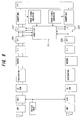
- Fig. 7 is a diagram of the structure of the cross-polarization interference canceller 205.
- the cross-polarization interference canceller 206 also has a similar structure.
- the cross-polarization interference canceller 205 which is constituted by a transversal filter, generates cross-polarization interference compensating signals Y IC , Y QC of Ich, Qch, and an adder 201f adds the cross-polarization interference compensating signals Y IC , Y QC to Ich signal Y I and Qch signal Y Q , thereby eliminating the interference components.
- the cross-polarization interference canceller 205 has a tap coefficient updater 501 and a FIR filter 502 in order to generate the cross-polarization interference compensating signal Y IC of Ich, and a tap coefficient updater 503 and a FIR filter 504 in order to generate the cross-polarization interference compensating signal Y QC of Qch.
- the tap coefficient updater 501 updates tap coefficients based upon an Ich signal X I of different polarization and an Ich component e I of an error signal and sets the tap coefficients in the FIR filter 502.
- the FIR filter 502 performs a convolutional operation between the Ich signal X I and tap coefficients, thereby generating the interference compensating signal Y IC of Ich.
- the tap coefficient updater 503 updates tap coefficients based upon a Qch signal X I of different polarization and a Qch component e Q of the error signal and sets the tap coefficients in the FIR filter 504.
- the FIR filter 504 performs a convolutional operation between the Qch signal X Q and tap coefficients, thereby generating the interference compensating signal Y QC of Qch.
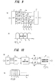
- Fig. 8 illustrates another example of the structure of an OFDM receiver apparatus.
- components identical with those of the OFDM receiver apparatus in Fig. 4 are designated by like reference characters.
- This structure differs in that it is adapted in such a manner that the cancellation of cross-polarization interference is performed after the FFT operation. Specifically, this structure differs in that:
- the scale of the canceller circuitry can be reduced by a wide margin. Accordingly, by using the cross-polarization interference compensating signal that is output from the canceller in common for each carrier, the overall circuit structure can be simplified.
- cross-polarization interference caused by a shift in antenna polarization angle or distortion in the transmission path conforming to rainfall and other factors can be eliminated by a cross-polarization interference canceller.
- the speed per symbol of each carrier becomes 1/N, where N represents the number of carriers, the amount of delay of interference waves becomes relatively small, the number of taps of a FIR constituting the canceller can be reduced and the scale of the circuitry can be reduced overall.
Landscapes
- Engineering & Computer Science (AREA)
- Signal Processing (AREA)
- Computer Networks & Wireless Communication (AREA)
- Noise Elimination (AREA)
- Radio Transmission System (AREA)
Applications Claiming Priority (1)
| Application Number | Priority Date | Filing Date | Title |
|---|---|---|---|
| PCT/JP2002/013261 WO2004057783A1 (ja) | 2002-12-19 | 2002-12-19 | Ofdm送受信装置 |
Publications (3)
| Publication Number | Publication Date |
|---|---|
| EP1575202A1 true EP1575202A1 (de) | 2005-09-14 |
| EP1575202A4 EP1575202A4 (de) | 2011-06-01 |
| EP1575202B1 EP1575202B1 (de) | 2015-03-18 |
Family
ID=32676912
Family Applications (1)
| Application Number | Title | Priority Date | Filing Date |
|---|---|---|---|
| EP02786143.4A Expired - Lifetime EP1575202B1 (de) | 2002-12-19 | 2002-12-19 | Ofdm-empfangsvorrichtung |
Country Status (3)
| Country | Link |
|---|---|
| EP (1) | EP1575202B1 (de) |
| JP (1) | JP4083746B2 (de) |
| WO (1) | WO2004057783A1 (de) |
Families Citing this family (3)
| Publication number | Priority date | Publication date | Assignee | Title |
|---|---|---|---|---|
| JP4672557B2 (ja) * | 2006-01-11 | 2011-04-20 | 日本電信電話株式会社 | 無線通信装置及び無線通信システム |
| WO2011138971A1 (ja) * | 2010-05-07 | 2011-11-10 | 日本電気株式会社 | 伝送装置、伝送方法及び伝送システム |
| JP5937961B2 (ja) * | 2012-07-11 | 2016-06-22 | 日本電信電話株式会社 | 光変調装置、光変調システム、及び光変調方法 |
Family Cites Families (11)
| Publication number | Priority date | Publication date | Assignee | Title |
|---|---|---|---|---|
| JPS5856545A (ja) * | 1981-09-30 | 1983-04-04 | Nec Corp | 偏波干渉除去回路 |
| JPS6124339A (ja) * | 1984-07-12 | 1986-02-03 | Nec Corp | 交差偏波補償方式 |
| US4727534A (en) * | 1986-08-19 | 1988-02-23 | American Telephone And Telegraph Company | Timing and carrier recovery in dual polarization communications systems |
| JP2737348B2 (ja) * | 1990-02-27 | 1998-04-08 | 日本電気株式会社 | 交差偏波干渉除去器 |
| FR2732178A1 (fr) * | 1995-03-22 | 1996-09-27 | Philips Electronique Lab | Systeme de transmission numerique muni d'un recepteur a egaliseurs cascades |
| JP2000022661A (ja) * | 1998-07-07 | 2000-01-21 | Nec Corp | Ofdm復調装置 |
| JP2000165339A (ja) * | 1998-11-27 | 2000-06-16 | Nec Corp | 送信lo同期方式を用いた両偏波伝送システム |
| JP2000183845A (ja) * | 1998-12-15 | 2000-06-30 | Telecommunication Advancement Organization Of Japan | 直交偏波マルチキャリア変復調方式の受信装置 |
| JP3678119B2 (ja) * | 2000-06-01 | 2005-08-03 | 株式会社デンソー | Ofdm用通信システムおよびその通信システムに用いられる基地局並びに端末 |
| WO2002019569A1 (en) * | 2000-08-30 | 2002-03-07 | Matsushita Electric Industrial Co., Ltd. | Data transmitting apparatus, radio communication system and radio communication method |
| KR100510434B1 (ko) * | 2001-04-09 | 2005-08-26 | 니폰덴신뎅와 가부시키가이샤 | Ofdm신호전달 시스템, ofdm신호 송신장치 및ofdm신호 수신장치 |
-
2002
- 2002-12-19 EP EP02786143.4A patent/EP1575202B1/de not_active Expired - Lifetime
- 2002-12-19 JP JP2004561990A patent/JP4083746B2/ja not_active Expired - Fee Related
- 2002-12-19 WO PCT/JP2002/013261 patent/WO2004057783A1/ja not_active Ceased
Also Published As
| Publication number | Publication date |
|---|---|
| EP1575202B1 (de) | 2015-03-18 |
| JPWO2004057783A1 (ja) | 2006-04-27 |
| JP4083746B2 (ja) | 2008-04-30 |
| EP1575202A4 (de) | 2011-06-01 |
| WO2004057783A1 (ja) | 2004-07-08 |
Similar Documents
| Publication | Publication Date | Title |
|---|---|---|
| US7551678B2 (en) | OFDM transceiver apparatus | |
| US10270574B2 (en) | Transmission signal generation apparatus, transmission signal generation method, reception signal apparatus, and reception signal method | |
| US10128899B2 (en) | Transmission device, reception device, and radio communication method | |
| US7643567B2 (en) | OFDM signal transmitting method and transmitter and receiver thereof | |
| CN1797988B (zh) | 无线通信装置和无线通信方法 | |
| US20120120935A1 (en) | Packet processing systems and methods | |
| US20100272199A1 (en) | Transmission device, reception device, and ofdm transmission method | |
| US11671304B2 (en) | Transmission method, transmission device, reception method, and reception device | |
| EP3427420B1 (de) | Verfahren und vorrichtung zur i-q-entkoppelten modulation und demodulation | |
| US20090092193A1 (en) | Multi carrier transmission device, multi carrier reception device, and communication method | |
| US10979276B2 (en) | Transmission method, transmission device, reception method, and reception device | |
| EP1575202B1 (de) | Ofdm-empfangsvorrichtung | |
| EP1819085A1 (de) | Vorrichtung und verfahren zum radiosenden und radioempfang | |
| KR20070091128A (ko) | 무선 통신 장치 및 데이터 다중 방법 | |
| JP4930262B2 (ja) | Ofdm受信装置及びofdm受信方法 |
Legal Events
| Date | Code | Title | Description |
|---|---|---|---|
| PUAI | Public reference made under article 153(3) epc to a published international application that has entered the european phase |
Free format text: ORIGINAL CODE: 0009012 |
|
| 17P | Request for examination filed |
Effective date: 20050517 |
|
| AK | Designated contracting states |
Kind code of ref document: A1 Designated state(s): AT BE BG CH CY CZ DE DK EE ES FI FR GB GR IE IT LI LU MC NL PT SE SI SK TR |
|
| RBV | Designated contracting states (corrected) |
Designated state(s): DE FR GB IT |
|
| A4 | Supplementary search report drawn up and despatched |
Effective date: 20110504 |
|
| RIC1 | Information provided on ipc code assigned before grant |
Ipc: H04L 27/26 20060101ALI20110428BHEP Ipc: H04J 11/00 20060101AFI20040715BHEP Ipc: H04B 1/00 20060101ALI20110428BHEP Ipc: H04L 5/04 20060101ALI20110428BHEP Ipc: H04B 7/10 20060101ALI20110428BHEP |
|
| 17Q | First examination report despatched |
Effective date: 20110902 |
|
| GRAP | Despatch of communication of intention to grant a patent |
Free format text: ORIGINAL CODE: EPIDOSNIGR1 |
|
| INTG | Intention to grant announced |
Effective date: 20140527 |
|
| GRAS | Grant fee paid |
Free format text: ORIGINAL CODE: EPIDOSNIGR3 |
|
| GRAP | Despatch of communication of intention to grant a patent |
Free format text: ORIGINAL CODE: EPIDOSNIGR1 |
|
| INTG | Intention to grant announced |
Effective date: 20141007 |
|
| GRAA | (expected) grant |
Free format text: ORIGINAL CODE: 0009210 |
|
| AK | Designated contracting states |
Kind code of ref document: B1 Designated state(s): DE FR GB IT |
|
| REG | Reference to a national code |
Ref country code: GB Ref legal event code: FG4D |
|
| REG | Reference to a national code |
Ref country code: DE Ref legal event code: R096 Ref document number: 60247043 Country of ref document: DE Effective date: 20150430 |
|
| REG | Reference to a national code |
Ref country code: FR Ref legal event code: PLFP Year of fee payment: 14 |
|
| REG | Reference to a national code |
Ref country code: DE Ref legal event code: R097 Ref document number: 60247043 Country of ref document: DE |
|
| PG25 | Lapsed in a contracting state [announced via postgrant information from national office to epo] |
Ref country code: IT Free format text: LAPSE BECAUSE OF FAILURE TO SUBMIT A TRANSLATION OF THE DESCRIPTION OR TO PAY THE FEE WITHIN THE PRESCRIBED TIME-LIMIT Effective date: 20150318 |
|
| PLBE | No opposition filed within time limit |
Free format text: ORIGINAL CODE: 0009261 |
|
| STAA | Information on the status of an ep patent application or granted ep patent |
Free format text: STATUS: NO OPPOSITION FILED WITHIN TIME LIMIT |
|
| 26N | No opposition filed |
Effective date: 20151221 |
|
| REG | Reference to a national code |
Ref country code: FR Ref legal event code: PLFP Year of fee payment: 15 |
|
| REG | Reference to a national code |
Ref country code: FR Ref legal event code: PLFP Year of fee payment: 16 |
|
| PGFP | Annual fee paid to national office [announced via postgrant information from national office to epo] |
Ref country code: FR Payment date: 20171113 Year of fee payment: 16 Ref country code: DE Payment date: 20171212 Year of fee payment: 16 |
|
| PGFP | Annual fee paid to national office [announced via postgrant information from national office to epo] |
Ref country code: GB Payment date: 20171213 Year of fee payment: 16 |
|
| REG | Reference to a national code |
Ref country code: DE Ref legal event code: R119 Ref document number: 60247043 Country of ref document: DE |
|
| GBPC | Gb: european patent ceased through non-payment of renewal fee |
Effective date: 20181219 |
|
| PG25 | Lapsed in a contracting state [announced via postgrant information from national office to epo] |
Ref country code: FR Free format text: LAPSE BECAUSE OF NON-PAYMENT OF DUE FEES Effective date: 20181231 Ref country code: DE Free format text: LAPSE BECAUSE OF NON-PAYMENT OF DUE FEES Effective date: 20190702 |
|
| PG25 | Lapsed in a contracting state [announced via postgrant information from national office to epo] |
Ref country code: GB Free format text: LAPSE BECAUSE OF NON-PAYMENT OF DUE FEES Effective date: 20181219 |