EP1575206A2 - Vorrichtung zur Datensynchronisierung - Google Patents
Vorrichtung zur Datensynchronisierung Download PDFInfo
- Publication number
- EP1575206A2 EP1575206A2 EP05004796A EP05004796A EP1575206A2 EP 1575206 A2 EP1575206 A2 EP 1575206A2 EP 05004796 A EP05004796 A EP 05004796A EP 05004796 A EP05004796 A EP 05004796A EP 1575206 A2 EP1575206 A2 EP 1575206A2
- Authority
- EP
- European Patent Office
- Prior art keywords
- data
- clock
- write
- shift register
- read
- Prior art date
- Legal status (The legal status is an assumption and is not a legal conclusion. Google has not performed a legal analysis and makes no representation as to the accuracy of the status listed.)
- Granted
Links
Images


Classifications
-
- G—PHYSICS
- G06—COMPUTING OR CALCULATING; COUNTING
- G06F—ELECTRIC DIGITAL DATA PROCESSING
- G06F1/00—Details not covered by groups G06F3/00 - G06F13/00 and G06F21/00
- G06F1/04—Generating or distributing clock signals or signals derived directly therefrom
- G06F1/12—Synchronisation of different clock signals provided by a plurality of clock generators
-
- G—PHYSICS
- G06—COMPUTING OR CALCULATING; COUNTING
- G06F—ELECTRIC DIGITAL DATA PROCESSING
- G06F13/00—Interconnection of, or transfer of information or other signals between, memories, input/output devices or central processing units
- G06F13/38—Information transfer, e.g. on bus
- G06F13/40—Bus structure
- G06F13/4004—Coupling between buses
- G06F13/4027—Coupling between buses using bus bridges
- G06F13/405—Coupling between buses using bus bridges where the bridge performs a synchronising function
- G06F13/4059—Coupling between buses using bus bridges where the bridge performs a synchronising function where the synchronisation uses buffers, e.g. for speed matching between buses
-
- G—PHYSICS
- G06—COMPUTING OR CALCULATING; COUNTING
- G06F—ELECTRIC DIGITAL DATA PROCESSING
- G06F5/00—Methods or arrangements for data conversion without changing the order or content of the data handled
- G06F5/06—Methods or arrangements for data conversion without changing the order or content of the data handled for changing the speed of data flow, i.e. speed regularising or timing, e.g. delay lines, FIFO buffers; over- or underrun control therefor
- G06F5/10—Methods or arrangements for data conversion without changing the order or content of the data handled for changing the speed of data flow, i.e. speed regularising or timing, e.g. delay lines, FIFO buffers; over- or underrun control therefor having a sequence of storage locations each being individually accessible for both enqueue and dequeue operations, e.g. using random access memory
-
- H—ELECTRICITY
- H04—ELECTRIC COMMUNICATION TECHNIQUE
- H04L—TRANSMISSION OF DIGITAL INFORMATION, e.g. TELEGRAPHIC COMMUNICATION
- H04L7/00—Arrangements for synchronising receiver with transmitter
- H04L7/0008—Synchronisation information channels, e.g. clock distribution lines
-
- H—ELECTRICITY
- H04—ELECTRIC COMMUNICATION TECHNIQUE
- H04L—TRANSMISSION OF DIGITAL INFORMATION, e.g. TELEGRAPHIC COMMUNICATION
- H04L7/00—Arrangements for synchronising receiver with transmitter
- H04L7/0016—Arrangements for synchronising receiver with transmitter correction of synchronization errors
- H04L7/005—Correction by an elastic buffer
Definitions
- the present invention relates to a data synchronization arrangement for exchanging clocked data between different clock domains running in a digital processing equipment at substantially the same clock frequency but at an arbitrary relative phase shift.
- a conventional solution to these problems is to use a FIFO memory as a temporary storage.
- incremented/decremented pointers are used that are synchronized to only one of the clock signals. This is not a fail-safe solution.
- the mean time between failures (MTBF) is a figure that depends on the phase relation between the clock signals and the frequency at which the FIFO memory is operated.
- the present invention provides a data synchronization arrangement that is fail-safe at high speed.
- the invention provides a data synchronization arrangement for exchanging clocked data between different clock domains running in a digital processing equipment at the same clock frequency but at an arbitrary relative phase shift.
- the data synchronization arrangement comprises a buffer memory with a predetermined limited number of memory locations each of which has a data write port and a data read port.
- a write select multiplexer has a data input receiving an input data stream synchronized with the clock from a first clock domain, one data output for each of said memory locations and connected to a respective data write port, and one write select input for each data output.
- a read select multiplexer has one data input for each of the memory locations and connected to a respective data read port, one read select input for each data input, and a data output supplying an output data stream synchronized with the clock from a second clock domain.
- a write select shift register has a number of stages corresponding to the predetermined number of memory locations and an output stage looped back to an input stage, each stage having an output connected to a respective one of the write select inputs of the write select multiplexer.
- the write select shift register is clocked with the clock from the first clock domain.
- a read select shift register has a number of stages corresponding to the predetermined number of memory locations, each stage having an output connected to a respective one of the read select inputs of the read select multiplexer.
- the read select shift register is clocked with the clock from the second clock domain.
- a bit synchronization circuit is provided for loading each shift register with a bit pattern that contains only one high logic value, the bit patterns in the shift registers having a relative offset.
- a data input stream synchronized with the clock of the first clock domain is applied to the data input of the write select multiplexer and a data output stream synchronized with the clock of the second clock domain is taken from the data output of the read select multiplexer.
- the bit synchronization circuit on each power-on of the arrangement, loads a bit pattern with only one high logic value into the write shift register, the read shift register initially containing only low logic values. A high logic value appearing in the most significant bit stage of the write shift register is then synchronized with the read clock and loaded into the least significant bit stage of the read shift register. In this way, a maximum offset between write and read operations is ensured for a given depth of the shift registers.
- the buffer memory has four memory locations, and the shift registers have four stages. With such a configuration, a delay of two or three, but at least two, read clock cycles is introduced between a write operation and a read operation for the same datum.
- a data synchronization arrangement is shown intended to be used for exchanging data between different clock domains running in a digital processing equipment at the same clock frequency but at an arbitrary relative phase shift between the clock signals. While the invention will be disclosed with reference to bits of data that are exchanged sequentially between single data lines, it should be understood that the same concepts are applicable to busses with parallel data lines.
- reference numeral 10 designates a 1-to-4 multiplexer referred to as a write select multiplexer.
- Write select multiplexer 10 has a serial data input WR_DATA and four data outputs. Data input WR_DATA receives a serial data input synchronized with a clock signal from a first clock domain.
- a buffer memory 12 has four memory locations, each memory location having a data write port and a data read port. Each data output of the write select multiplexer 10 is connected to one data write port of a buffer memory 12.
- Each data read port of buffer memory 10 is connected to one out of four data inputs of a 4-to-1 multiplexer 14, referred to as a read select multiplexer.
- Read select multiplexer 14 has a serial data output that provides an output data stream RD_DATA that is synchronized with a clock signal from a second clock domain, as will be explained further.
- Write select multiplexer 10 has four write select inputs each of which is connected to an output of one out of four stages of a write select shift register 16.
- the output of the MSB (most significant bit) stage of shift register 16 is looped back to the input of the LSB (least significant bit) stage.
- Write select shift register 16 is clocked by the clock signal from the first clock domain, referred to as write clock WR_CLK.
- Read select multiplexer 14 has four read select inputs each of which is connected to an output of one out of four stages of a read select shift register 18.
- Read select shift register 18 is clocked by the clock signal from the second clock domain, referred to as read clock RD_CLK.
- a bit synchronization circuit 20 is inserted between the output of the MSB (most significant bit) stage of write select shift register 10 and the input of the LSB (least significant bit) stage of read select shift register.
- the bit synchronization circuit 20 is effective to introduce a fixed offset between bit patterns loaded into shift registers 16 and 18 and to keep the offset constant throughout operation of the arrangement. At any time, the bit pattern in write shift register 16 has only one high value. On power-on of the arrangement, a high logic value is loaded into the least significant bit stage and low logic values are loaded in the three remaining stages of write select register 16, and low logic values are loaded into all the stages of the read select shift register 18. This reset condition is illustrated in Fig. 1.
- bit synchronization circuit 20 introduces a delay of two or three, but at least two, read clock cycles before the synchronized bit enters the read select shift register 18.
- the constant offset between the bit patterns in both shift registers introduces a corresponding delay between a write and a read operation for the same data in buffer memory 12. In other words, memory locations that are addressed for reading have been written to at least two read clock cycles before, and never can a memory location be read from while data are written to it.
- the clock frequencies are allowed to differ slightly, although generally not more than about one percent.
- more than only one logic high value may momentarily happen to occur in the four stages of read select shift register 18.
- the logic states of all stages in read select shift register 18 are monitored by an associated logic monitoring circuit 22.
- the logic monitoring circuit 22 discards one of them, preferably the one in a more significant stage, so that only one high value will remain in the shift register after the next shift procedure. This avoids data to be read from different stages of buffer memory 12 at the same time, although one datum from the input data stream will be lost.
- the write clock WR_CLK has a lower frequency, a situation may momentarily occur where all four stages of read select shift register 8 have a logic low value. In that case, a datum is inserted in the output data stream.
- clock signals WR_CLK and RD_CLK are seen to have the same frequency and a relative phase shift of ⁇ /2.
- Signal S 1 in Fig. 2 represents a pulse sequence that appears at the MSB output of write select shift register 16. It has a frequency of the clock frequency divided by four, and a duty cycle of 1:4.
- This signal S 1 is converted by the bit synchronization circuit 20 into a signal S2 that toggles with each high pulse of signal S 1 in synchronism with the write clock WR_CLK.
- Signal S2 has only half the frequency of signal S1.
- Signal S2 is then synchronized with the read clock RD_CLK by a two-stages synchronizer within circuit 20, as illustrated by signals S3 and S4 in Fig. 2a.
- a suitable synchronizer may be built with two flip-flops clocked with the read clock RD_CLK.
- Signal S5 is signal S4 shifted by one clock cycle
- signal S6 is a pulse signal generated from signal S5 to be analogous with signal S1.
- the pulse sequence represented by signal S6 is shifted into the read shift register.
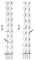
- Fig. 2b illustrates a situation where the write clock WR_CLK has a slightly higher frequency than the read clock RD_CLK. As is seen, one datum may be dropped occasionally, due to the necessity of discarding one out of two logic high values appearing simultaneously at read select shift register 18. In Fig. 2b, datum "080" is lost from the input data stream WR_DATA.
- Fig. 2c illustrates a situation where the write clock WR_CLK has a slightly lower frequency than the read clock RD_CLK. As is seen, one datum "2AA" is inserted into the input data stream WR_DATA.
- the buffer memory 12 is formed by a set of single registers or by a bank of registers; each register may be formed by a D-Flip-Flop.
- the arrangement disclosed may be considered as a serial interface with input WR_DATA and output RD_DATA in case serial data are exchanged.
- each bus line needs a buffer memory and a multiplexer as disclosed, but only one select mechanism with a write select shift register and a read select shift register is required for all bus lines.
Landscapes
- Engineering & Computer Science (AREA)
- Theoretical Computer Science (AREA)
- General Engineering & Computer Science (AREA)
- Physics & Mathematics (AREA)
- General Physics & Mathematics (AREA)
- Computer Networks & Wireless Communication (AREA)
- Signal Processing (AREA)
- Computer Hardware Design (AREA)
- Synchronisation In Digital Transmission Systems (AREA)
- Time-Division Multiplex Systems (AREA)
Applications Claiming Priority (2)
| Application Number | Priority Date | Filing Date | Title |
|---|---|---|---|
| DE102004011673 | 2004-03-10 | ||
| DE102004011673A DE102004011673B3 (de) | 2004-03-10 | 2004-03-10 | Vorrichtung zur Datensynchronisation |
Publications (3)
| Publication Number | Publication Date |
|---|---|
| EP1575206A2 true EP1575206A2 (de) | 2005-09-14 |
| EP1575206A3 EP1575206A3 (de) | 2006-04-05 |
| EP1575206B1 EP1575206B1 (de) | 2017-10-25 |
Family
ID=34530468
Family Applications (1)
| Application Number | Title | Priority Date | Filing Date |
|---|---|---|---|
| EP05004796.8A Ceased EP1575206B1 (de) | 2004-03-10 | 2005-03-04 | Vorrichtung zur Datensynchronisierung |
Country Status (3)
| Country | Link |
|---|---|
| US (1) | US7350092B2 (de) |
| EP (1) | EP1575206B1 (de) |
| DE (1) | DE102004011673B3 (de) |
Families Citing this family (7)
| Publication number | Priority date | Publication date | Assignee | Title |
|---|---|---|---|---|
| WO2008129364A1 (en) * | 2007-04-23 | 2008-10-30 | Nokia Corporation | Transferring data between asynchronous clock domains |
| US9324416B2 (en) * | 2014-08-20 | 2016-04-26 | Qualcomm Incorporated | Pseudo dual port memory with dual latch flip-flop |
| SE1730348A1 (sv) * | 2017-12-20 | 2019-02-26 | Totalfoersvarets Forskningsinstitut | Metod, system och datorprogram för synkronisering av dataströmmar med okänd fördröjning |
| US10395702B1 (en) | 2018-05-11 | 2019-08-27 | Micron Technology, Inc. | Memory device with a clocking mechanism |
| CN119126919A (zh) * | 2018-10-24 | 2024-12-13 | 奇跃公司 | 异步asic |
| JP2020166346A (ja) * | 2019-03-28 | 2020-10-08 | ラピスセミコンダクタ株式会社 | 半導体記憶装置 |
| US11829640B2 (en) | 2020-10-27 | 2023-11-28 | Rambus Inc. | Asynchronous arbitration across clock domains for register writes in an integrated circuit chip |
Family Cites Families (12)
| Publication number | Priority date | Publication date | Assignee | Title |
|---|---|---|---|---|
| US4463443A (en) * | 1979-07-24 | 1984-07-31 | The United States Of America As Represented By The Secretary Of The Air Force | Data buffer apparatus between subsystems which operate at differing or varying data rates |
| EP0574598A1 (de) * | 1992-06-13 | 1993-12-22 | International Business Machines Corporation | Datenpufferspeicher |
| US5473756A (en) * | 1992-12-30 | 1995-12-05 | Intel Corporation | FIFO buffer with full/empty detection by comparing respective registers in read and write circular shift registers |
| US5602878A (en) * | 1994-09-23 | 1997-02-11 | Intel Corporation | Method of delivering stable data across an asynchronous interface |
| WO1999019785A1 (en) * | 1997-10-10 | 1999-04-22 | Rambus Incorporated | Apparatus and method for generating a distributed clock signal using gear ratio techniques |
| US6041370A (en) * | 1997-12-08 | 2000-03-21 | Intel Corporation | FIFO using a fading ones counter |
| US6724846B1 (en) * | 2000-04-28 | 2004-04-20 | Hewlett-Packard Development Company, L.P. | Simple, high performance, bit-sliced mesochronous synchronizer for a source synchronous link |
| US6920578B1 (en) * | 2001-12-18 | 2005-07-19 | Lsi Logic Corporation | Method and apparatus for transferring data between a slower clock domain and a faster clock domain in which one of the clock domains is bandwidth limited |
| US6724683B2 (en) * | 2002-03-06 | 2004-04-20 | Applied Micro Circuits Corporation | Transferring data between different clock domains |
| US7134035B2 (en) * | 2003-05-30 | 2006-11-07 | Sun Mircosystems, Inc. | Method for generating a synchronization signal based on the clock ratio between two clock domains for data transfer between the domains |
| US7392417B2 (en) * | 2003-10-06 | 2008-06-24 | Nxp B.V. | Device for exchanging data signals between two clock domains |
| DE102004011672B4 (de) * | 2004-03-10 | 2007-04-05 | Texas Instruments Deutschland Gmbh | Vorrichtung zur Datensynchronisation |
-
2004
- 2004-03-10 DE DE102004011673A patent/DE102004011673B3/de not_active Expired - Fee Related
-
2005
- 2005-03-04 EP EP05004796.8A patent/EP1575206B1/de not_active Ceased
- 2005-03-08 US US11/074,443 patent/US7350092B2/en not_active Expired - Lifetime
Also Published As
| Publication number | Publication date |
|---|---|
| US7350092B2 (en) | 2008-03-25 |
| DE102004011673B3 (de) | 2005-06-02 |
| EP1575206B1 (de) | 2017-10-25 |
| EP1575206A3 (de) | 2006-04-05 |
| US20050201163A1 (en) | 2005-09-15 |
Similar Documents
| Publication | Publication Date | Title |
|---|---|---|
| JP2610213B2 (ja) | 同期装置及び同期方法 | |
| JP3565600B2 (ja) | データ通信装置およびデータ通信方法 | |
| US6963220B2 (en) | Methods and circuitry for implementing first-in first-out structure | |
| US8301932B2 (en) | Synchronising between clock domains | |
| US7310396B1 (en) | Asynchronous FIFO buffer for synchronizing data transfers between clock domains | |
| US7003423B1 (en) | Programmable logic resource with data transfer synchronization | |
| EP0226017B1 (de) | Datensynchronisator zwischen einer Sende- und einer Empfangsanlage | |
| US8520464B2 (en) | Interface circuit and semiconductor device incorporating same | |
| US8132036B2 (en) | Reducing latency in data transfer between asynchronous clock domains | |
| JP3645584B2 (ja) | データ転送同期装置 | |
| US7242737B2 (en) | System and method for data phase realignment | |
| EP3739463B1 (de) | Schaltung zur asynchronen datenübertragung | |
| US7500132B1 (en) | Method of asynchronously transmitting data between clock domains | |
| US7350092B2 (en) | Data synchronization arrangement | |
| US6075833A (en) | Method and apparatus for counting signal transitions | |
| US7145831B2 (en) | Data synchronization arrangement | |
| US8363766B2 (en) | Device and method of synchronizing signals | |
| CN100405253C (zh) | 数据传送同步化电路、方法及计算机 | |
| EP1317085A2 (de) | Verfahren und Schaltung zur Initialisierung eines Laufzeitausgleichpuffers in einem taktweitergeleiteten System | |
| JP3562416B2 (ja) | Lsi間データ転送システム及びそれに用いるソースシンクロナスデータ転送方式 | |
| JP2000353939A (ja) | クロック信号同期式フリップフロップ回路 | |
| JP2596336B2 (ja) | 非同期ディジタル通信装置 | |
| US6470459B1 (en) | Half-word synchronization method for internal clock | |
| GB2228848A (en) | A data synchronisation arrangement | |
| JP2000183859A (ja) | スリップ制御装置 |
Legal Events
| Date | Code | Title | Description |
|---|---|---|---|
| PUAI | Public reference made under article 153(3) epc to a published international application that has entered the european phase |
Free format text: ORIGINAL CODE: 0009012 |
|
| AK | Designated contracting states |
Kind code of ref document: A2 Designated state(s): AT BE BG CH CY CZ DE DK EE ES FI FR GB GR HU IE IS IT LI LT LU MC NL PL PT RO SE SI SK TR |
|
| AX | Request for extension of the european patent |
Extension state: AL BA HR LV MK YU |
|
| PUAL | Search report despatched |
Free format text: ORIGINAL CODE: 0009013 |
|
| AK | Designated contracting states |
Kind code of ref document: A3 Designated state(s): AT BE BG CH CY CZ DE DK EE ES FI FR GB GR HU IE IS IT LI LT LU MC NL PL PT RO SE SI SK TR |
|
| AX | Request for extension of the european patent |
Extension state: AL BA HR LV MK YU |
|
| RIC1 | Information provided on ipc code assigned before grant |
Ipc: G06F 5/00 20060101ALI20060210BHEP Ipc: H04L 7/00 20060101AFI20050527BHEP |
|
| AKX | Designation fees paid | ||
| 17P | Request for examination filed |
Effective date: 20061211 |
|
| RBV | Designated contracting states (corrected) |
Designated state(s): DE FR GB |
|
| 17Q | First examination report despatched |
Effective date: 20071121 |
|
| GRAP | Despatch of communication of intention to grant a patent |
Free format text: ORIGINAL CODE: EPIDOSNIGR1 |
|
| INTG | Intention to grant announced |
Effective date: 20170421 |
|
| GRAS | Grant fee paid |
Free format text: ORIGINAL CODE: EPIDOSNIGR3 |
|
| GRAJ | Information related to disapproval of communication of intention to grant by the applicant or resumption of examination proceedings by the epo deleted |
Free format text: ORIGINAL CODE: EPIDOSDIGR1 |
|
| GRAL | Information related to payment of fee for publishing/printing deleted |
Free format text: ORIGINAL CODE: EPIDOSDIGR3 |
|
| GRAR | Information related to intention to grant a patent recorded |
Free format text: ORIGINAL CODE: EPIDOSNIGR71 |
|
| GRAA | (expected) grant |
Free format text: ORIGINAL CODE: 0009210 |
|
| INTC | Intention to grant announced (deleted) | ||
| AK | Designated contracting states |
Kind code of ref document: B1 Designated state(s): DE FR GB |
|
| INTG | Intention to grant announced |
Effective date: 20170919 |
|
| REG | Reference to a national code |
Ref country code: GB Ref legal event code: FG4D |
|
| REG | Reference to a national code |
Ref country code: DE Ref legal event code: R096 Ref document number: 602005052928 Country of ref document: DE |
|
| REG | Reference to a national code |
Ref country code: FR Ref legal event code: PLFP Year of fee payment: 14 |
|
| REG | Reference to a national code |
Ref country code: DE Ref legal event code: R097 Ref document number: 602005052928 Country of ref document: DE |
|
| PLBE | No opposition filed within time limit |
Free format text: ORIGINAL CODE: 0009261 |
|
| STAA | Information on the status of an ep patent application or granted ep patent |
Free format text: STATUS: NO OPPOSITION FILED WITHIN TIME LIMIT |
|
| 26N | No opposition filed |
Effective date: 20180726 |
|
| PGFP | Annual fee paid to national office [announced via postgrant information from national office to epo] |
Ref country code: GB Payment date: 20200228 Year of fee payment: 16 Ref country code: DE Payment date: 20200214 Year of fee payment: 16 |
|
| PGFP | Annual fee paid to national office [announced via postgrant information from national office to epo] |
Ref country code: FR Payment date: 20200219 Year of fee payment: 16 |
|
| REG | Reference to a national code |
Ref country code: DE Ref legal event code: R119 Ref document number: 602005052928 Country of ref document: DE |
|
| GBPC | Gb: european patent ceased through non-payment of renewal fee |
Effective date: 20210304 |
|
| PG25 | Lapsed in a contracting state [announced via postgrant information from national office to epo] |
Ref country code: GB Free format text: LAPSE BECAUSE OF NON-PAYMENT OF DUE FEES Effective date: 20210304 Ref country code: FR Free format text: LAPSE BECAUSE OF NON-PAYMENT OF DUE FEES Effective date: 20210331 Ref country code: DE Free format text: LAPSE BECAUSE OF NON-PAYMENT OF DUE FEES Effective date: 20211001 |