EP1576356B1 - Appareil et procede pour creer des repartitions de champs electromagnetiques - Google Patents
Appareil et procede pour creer des repartitions de champs electromagnetiques Download PDFInfo
- Publication number
- EP1576356B1 EP1576356B1 EP03775037A EP03775037A EP1576356B1 EP 1576356 B1 EP1576356 B1 EP 1576356B1 EP 03775037 A EP03775037 A EP 03775037A EP 03775037 A EP03775037 A EP 03775037A EP 1576356 B1 EP1576356 B1 EP 1576356B1
- Authority
- EP
- European Patent Office
- Prior art keywords
- layer
- structured layer
- platform
- substrate
- electromagnetic
- Prior art date
- Legal status (The legal status is an assumption and is not a legal conclusion. Google has not performed a legal analysis and makes no representation as to the accuracy of the status listed.)
- Expired - Lifetime
Links
Images

Classifications
-
- G—PHYSICS
- G01—MEASURING; TESTING
- G01N—INVESTIGATING OR ANALYSING MATERIALS BY DETERMINING THEIR CHEMICAL OR PHYSICAL PROPERTIES
- G01N21/00—Investigating or analysing materials by the use of optical means, i.e. using sub-millimetre waves, infrared, visible or ultraviolet light
- G01N21/75—Systems in which material is subjected to a chemical reaction, the progress or the result of the reaction being investigated
- G01N21/77—Systems in which material is subjected to a chemical reaction, the progress or the result of the reaction being investigated by observing the effect on a chemical indicator
- G01N21/7703—Systems in which material is subjected to a chemical reaction, the progress or the result of the reaction being investigated by observing the effect on a chemical indicator using reagent-clad optical fibres or optical waveguides
- G01N21/774—Systems in which material is subjected to a chemical reaction, the progress or the result of the reaction being investigated by observing the effect on a chemical indicator using reagent-clad optical fibres or optical waveguides the reagent being on a grating or periodic structure
- G01N21/7743—Systems in which material is subjected to a chemical reaction, the progress or the result of the reaction being investigated by observing the effect on a chemical indicator using reagent-clad optical fibres or optical waveguides the reagent being on a grating or periodic structure the reagent-coated grating coupling light in or out of the waveguide
-
- G—PHYSICS
- G02—OPTICS
- G02B—OPTICAL ELEMENTS, SYSTEMS OR APPARATUS
- G02B5/00—Optical elements other than lenses
- G02B5/18—Diffraction gratings
-
- G—PHYSICS
- G01—MEASURING; TESTING
- G01N—INVESTIGATING OR ANALYSING MATERIALS BY DETERMINING THEIR CHEMICAL OR PHYSICAL PROPERTIES
- G01N21/00—Investigating or analysing materials by the use of optical means, i.e. using sub-millimetre waves, infrared, visible or ultraviolet light
- G01N21/17—Systems in which incident light is modified in accordance with the properties of the material investigated
- G01N21/47—Scattering, i.e. diffuse reflection
- G01N21/4788—Diffraction
-
- G—PHYSICS
- G01—MEASURING; TESTING
- G01N—INVESTIGATING OR ANALYSING MATERIALS BY DETERMINING THEIR CHEMICAL OR PHYSICAL PROPERTIES
- G01N21/00—Investigating or analysing materials by the use of optical means, i.e. using sub-millimetre waves, infrared, visible or ultraviolet light
- G01N21/17—Systems in which incident light is modified in accordance with the properties of the material investigated
- G01N21/55—Specular reflectivity
-
- G—PHYSICS
- G01—MEASURING; TESTING
- G01N—INVESTIGATING OR ANALYSING MATERIALS BY DETERMINING THEIR CHEMICAL OR PHYSICAL PROPERTIES
- G01N21/00—Investigating or analysing materials by the use of optical means, i.e. using sub-millimetre waves, infrared, visible or ultraviolet light
- G01N21/62—Systems in which the material investigated is excited whereby it emits light or causes a change in wavelength of the incident light
- G01N21/63—Systems in which the material investigated is excited whereby it emits light or causes a change in wavelength of the incident light optically excited
- G01N21/64—Fluorescence; Phosphorescence
- G01N21/645—Specially adapted constructive features of fluorimeters
- G01N21/6452—Individual samples arranged in a regular 2D-array, e.g. multiwell plates
-
- G—PHYSICS
- G01—MEASURING; TESTING
- G01N—INVESTIGATING OR ANALYSING MATERIALS BY DETERMINING THEIR CHEMICAL OR PHYSICAL PROPERTIES
- G01N21/00—Investigating or analysing materials by the use of optical means, i.e. using sub-millimetre waves, infrared, visible or ultraviolet light
- G01N21/75—Systems in which material is subjected to a chemical reaction, the progress or the result of the reaction being investigated
- G01N21/77—Systems in which material is subjected to a chemical reaction, the progress or the result of the reaction being investigated by observing the effect on a chemical indicator
- G01N21/7703—Systems in which material is subjected to a chemical reaction, the progress or the result of the reaction being investigated by observing the effect on a chemical indicator using reagent-clad optical fibres or optical waveguides
- G01N21/774—Systems in which material is subjected to a chemical reaction, the progress or the result of the reaction being investigated by observing the effect on a chemical indicator using reagent-clad optical fibres or optical waveguides the reagent being on a grating or periodic structure
-
- G—PHYSICS
- G01—MEASURING; TESTING
- G01N—INVESTIGATING OR ANALYSING MATERIALS BY DETERMINING THEIR CHEMICAL OR PHYSICAL PROPERTIES
- G01N27/00—Investigating or analysing materials by the use of electric, electrochemical, or magnetic means
-
- G—PHYSICS
- G02—OPTICS
- G02B—OPTICAL ELEMENTS, SYSTEMS OR APPARATUS
- G02B5/00—Optical elements other than lenses
-
- G—PHYSICS
- G01—MEASURING; TESTING
- G01N—INVESTIGATING OR ANALYSING MATERIALS BY DETERMINING THEIR CHEMICAL OR PHYSICAL PROPERTIES
- G01N21/00—Investigating or analysing materials by the use of optical means, i.e. using sub-millimetre waves, infrared, visible or ultraviolet light
- G01N21/75—Systems in which material is subjected to a chemical reaction, the progress or the result of the reaction being investigated
- G01N21/77—Systems in which material is subjected to a chemical reaction, the progress or the result of the reaction being investigated by observing the effect on a chemical indicator
- G01N21/7703—Systems in which material is subjected to a chemical reaction, the progress or the result of the reaction being investigated by observing the effect on a chemical indicator using reagent-clad optical fibres or optical waveguides
- G01N21/7746—Systems in which material is subjected to a chemical reaction, the progress or the result of the reaction being investigated by observing the effect on a chemical indicator using reagent-clad optical fibres or optical waveguides the waveguide coupled to a cavity resonator
Definitions
- the present invention relates to an apparatus and a method for generating electromagnetic fields in areas accessible for substances to be exposed.
- the invention relates to optical sensors for measuring biological or chemical substances.
- Electromagnetic fields are used in a variety of applications for the detection of small concentrations of substances in a mostly liquid sample.
- the optical sensors which are based on the detection of substances deposited on the surface of the sensor, basically two classes are distinguished: those that work with labeled substances (label methods) and those that do without the label (label-free methods).
- a method can be classified in which the substances to be detected are labeled with a fluorescent dye.
- fluorescent dyes are, for example, CY5 for an excitation wavelength of 532nm and CY3 for an excitation wavelength of around 635nm.
- This label may be selective, but generally also affects other substances present in a sample to be measured. If the label is not selective, then selection can then be achieved, for example, by preparing the surface of the sensor in such a way that only the labeled substance to be measured is selectively bound to this surface. If, after completion of the binding, the surface is rinsed, the result is a quantitative statement about the concentration of the substance to be measured in the test sample via the strength of the resulting fluorescence signal. A quantitative statement can also be made without rinsing if it is achieved that a fluorescence exciting electromagnetic field is bound to the surface to which the substances to be detected, concentrated and essentially limited to this.
- the substance to be measured has a direct influence on the field distribution in the sensor, for example as a result of a change in the refractive index which it causes when it attaches to the surface of the sensor.
- This influence affects optical parameters such as diffraction efficiencies or, if applicable, the guided waves in a waveguide and causes measurable changes.
- TIR total internal reflection
- a cross-attenuated field is created on the surface, which protrudes exponentially downwards into the medium to be measured away from the substrate.
- such fields are also referred to as evanescent fields since no light is propagated into the medium to be measured but merely "protrudes" into it, ie. the field is limited to the immediate vicinity of the corresponding interface.
- the so-called penetration depth ie the distance from the interface at which the field strength has dropped to 1 / e (where e is the Euler number), depends, inter alia, on the actual angle of incidence and is typically expressed in units the vacuum wavelength of the exciting light is measured and is of the same order of magnitude.
- An example of the use of evanescent wave in sensors is in WO98 / 08219 given by John Guerra.
- a so-called phase-controlled evanescent field is exploited, the planes of constant phase being substantially perpendicular to the object surface.
- the field is generated by means of TIR and is not excessive.
- the waveguiding layer ie, the layer in which the lightwave is guided, has a refractive index higher than the refractive indices of the substrate and the medium adjacent to the waveguiding layer. If this is not the case, then there is no multiple total reflection and thus not waveguiding (see for example WO 86/071149 ). For a given substrate, therefore, the choice of materials for the waveguiding layer is limited to high-index materials.
- Another difficulty is the coupling of the light into the waveguide, which can be achieved, inter alia, by means of front-side loading, prism coupling or coupling grating. In all the cases mentioned above, it is difficult to realize a constant coupling efficiency, but this should preferably be achieved for a quantitative statement.
- the density of the different measuring ranges is limited due to the extension of the waveguide.
- the well-known effect of the resonant grid with abnormal transmission breakdowns is exploited, such as in WO2001 / 002839 described by Novartis (hereinafter referred to as the Novartis application).
- a layer is applied to the substrate whose refractive index is higher than the refractive index of the substrate. Otherwise, the resonant effect does not occur.
- the patch area of the surface is defined by periodic trenches.
- the dimensioning of the structures and layers is selected so that when subjected to coherent light at a certain angle, a resonance effect occurs in which the transmission is abnormally reduced and the desired evanescent field is built up.
- This has the advantage that light does not have to propagate in a waveguide mode over a long distance and therefore the device is much less susceptible to impurities and scattering centers.
- the system chosen smaller and thus the number of measuring ranges can be greatly increased because the light propagates substantially not laterally.
- This advantage of the potentially increased measuring range density was found especially in W02000 / 75644 by Zeptosens (hereinafter referred to as Zeptosens application). Also in the Zeptosens application continuous modulation in the measuring range are realized, although it is still assumed that an optical slab waveguide.
- the object of the present invention is to specify a device by means of which an excessive field strength can be achieved, wherein the maximum field strength accessible to the measurement substance should not only include the evanescent components of the field strengths that build up in the device.
- Another aspect of the present invention is the realization of the high, not exclusively evanescent field strengths in surface layers whose refractive index is not or only slightly higher ( ⁇ 1%) than the refractive index of the substrate. It is also a task to provide the present invention, a method according to which such a field strength can be achieved.
- An embodiment of the platform is further characterized in that the refractive index or optionally the effective refractive index of the structured layer is less than 1% higher, but preferably smaller than the refractive index of the substrate.
- a further embodiment of the platform is further characterized in that the structure of the structured layer comprises substantially periodically arranged indentations forming part of the coupling means.
- a further embodiment of the platform is further characterized in that the multilayer system comprises metallic layers, preferably of Al, Ag, Au, their combination or other suitable materials.
- a further embodiment of the platform is characterized in that the layer system comprises dielectric layers and preferably no metallic layers, wherein the layer system is preferably constructed in alternating-layer construction in which high and low-index layers are arranged alternately.
- FIG. 1 Further embodiments of the platform are characterized in that the type of structuring, the coupling means, and the number and the material and the thickness distribution of the layers of the multilayer system are chosen so that the field strength distribution building up with suitable exposure of the platform to electromagnetic radiation in the stratum material-free Areas of the structured layer has at least one maximum.
- a field distribution platform can be generated which additionally comprises a source for the generation of electromagnetic radiation and an electromagnetic field whose field strength in the region of the structured layer is maximum.
- the electromagnetic field distribution in the layer-material-free regions of the structured layer has at least one maximum.
- the aforementioned platforms and field distribution platforms may be part of a sensor for measuring specific substances in a biological and / or chemical and / or biochemical sample.
- the aim of the optimization is to achieve an electromagnetic field distribution which has at least one maximum in the stratified material-free regions of the structured layer.
- the object is thus achieved by clever combination of the properties of dielectric multilayer systems and of optical gratings.
- the principle of waveguiding in high refractive layers as well as the principle of anomalous reduction of the transmission of resonant gratings is abandoned.
- a dielectric alternating layer system is arranged on the substrate, on which a diffraction grating is provided.
- such a system is only or additionally optimized to the effect that in the area of the surface structures and in particular in the region of the grid trenches the optimized system has a high or even the highest field strength.
- Such a procedure leads to systems in which, when exposed to the electromagnetic radiation used for the optimization, a field distribution builds up which has maxima in the grid trenches accessible for the measurement.
- both local optimization methods and global methods are suitable, both of which are familiar to the person skilled in the art of optical coatings, e.g. are sufficiently known for the optimization of optical alternating layer systems.
- the application of such optimization methods in connection with the present optimization goal is new and inventive.
- the skilled person knows how to proceed, as soon as the new aspect has been revealed to him, that he should optimize the electromagnetic field strength in certain areas of the structure and in this regard set the system parameters as optimization parameters, in particular the layer thicknesses and the grid depth. This completely reveals the doctrine of technical action.
- the multilayer system can be regarded as a means for decoupling the structured layer from the substrate with respect to higher orders of diffraction. Coupling and decoupling electromagnetic radiation into or out of the patterned layer is then essentially limited to the zeroth diffraction orders in transmission or reflection. This can lead to the build-up of high electromagnetic fields within the patterned layer, especially in the case of low diffraction efficiency diffraction structures.
- Such a field distribution can be achieved in particular with a system whose homogeneous layer on which the grating is arranged and / or whose grating structure may consist of a low-refractive material and in particular of a material whose refractive index is less than or equal to the refractive index of the substrate.
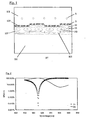
- FIG. 1 shown schematically.
- the refractive index of the layer is significantly higher than the refractive index of the substrate.
- the lattice structure of the substrate is transferred to the surface, which forms the termination to the surrounding medium, referred to below as superstrate 113.
- biological binding molecules 109 as found, for example, in an antibody-antigen reaction.
- This angle corresponds to the resonance angle of the Systems where the transmission is abnormally reduced.
- the admission takes place from the Superstratseite.
- the loading is carried out in such a way that the grid webs pierce this plane of incidence perpendicular, that is, in the example considered here is not conical loading.
- the TE polarization is characterized in that the electric field vector oscillates in the plane perpendicular to the plane of incidence.
- dashed lines are additionally drawn in the lines represent equal amplitude square of the field distribution.
- the corresponding reference numerals 5, 10, 15, and 20 indicate the corresponding values of the amplitude square. All data relating in this document to values of the amplitude squares are indications relative to the amplitude square of a plane wave. In other words, the light which is acted upon is an amplitude square of 1.
- Reference numerals are drawn only for one of the maxima. It is striking that the maxima of the amplitude square are embedded completely inaccessible to the substances to be measured in the high refractive index layer and the biological coupling elements only feel the evanescent foothills of the field.
- FIG. 2 Considering the diffraction efficiencies as a function of wavelength, shown in FIG. 2 , it is clear that all applied energy in this case is concentrated in the zeroth diffraction orders. This is the basis of the resonant effect used in the prior art.
- a reflection of almost 100% is achieved, while the transmission correspondingly decreases to nearly 0%, ie the effect of the anomalous reduction of the transmission is recognizable at 633 nm.
- FIG. 2 is used to illustrate the resonant effect of a logarithmic scale.
- a dielectric layer system 17 is applied with 6 layers.
- the layer system ends with a topmost SiO 2 layer. Applied to this layer is a periodic lattice structure. The grating period is 550nm.
- n 1, ie air or vacuum or the like.
- the grid trenches are therefore freely accessible for applying and attaching measuring substances.
- the admission takes place from the Superstratseite.
- the incident light beam together with the surface normal to the last layer, spans the plane of incidence.
- the loading is carried out in such a way that the grid webs pierce this plane of incidence perpendicular, that is, in the example considered here is not conical incidence.
- the TE polarization is characterized in that the electric field vector oscillates in the plane perpendicular to the plane of incidence.
- Table 1 refractive index Layer thickness or grid depth [nm] example superstrate 1 - air grid 1.48 and 1 387 SiO2 and air Layer 6 1:48 10.3 SiO 2 Layer 5 2:35 74.6 TiO 2 Layer 4 1:48 129.6 SiO 2 Layer 3 2:35 76.3 TiO 2 Layer 2 1:48 127.9 SiO 2 Layer 1 2:35 75.7 TiO 2 substratum 1:52 - BK7
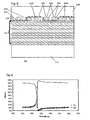
- FIG. 3 The system 11 shown in the example is shown schematically. Applied to the substrate is the layer system 17 consisting of 6 layers. On this layer system 17, a grid structure 19 is realized which includes both grid bars 23 and grid trenches 29. The grating period is 550nm.
- binding molecules 31 which sit at the bottom of the trench, optionally such binding molecules 31 'which are attached to the side walls and optionally such binding molecules 31''sitting on the lattice webs.
- other grid profiles such as sinusoidal or overhanging profiles are possible, where coupling elements can be fixed everywhere.
- dashed lines are additionally drawn in the lines represent equal amplitude square of the field distribution.
- the corresponding reference numerals 50, 100, 150 and 200 indicate the corresponding values of the amplitude square. It is noteworthy that in the trenches 29 of the lattice structure a maximum amplitude square of more than 200 is reached. These maxima are significantly higher than in the prior art and in contrast to this fully accessible to the measuring substances.
- the whole maximum field distribution is limited to the area of the grid.
- This is also a new system compared to the prior art, because the materials forming the lattice each have a refractive index which is not above the refractive index of the substrate and may even be significantly lower.
- the system 211 includes a substrate 223, a layer system 227, a grating region 229 having a period of 550nm, biological coupling elements 233, 233 ', 233 ", and a superstrate 239.
- the type of light applied is similar to that of the first example.
- the goal of the optimization was the requirement that To keep reflection accordingly low while still high field strength in the grid trenches.
- the system was set up according to the system described in the first example, where 16 layers were used for the optimization and instead of TiO2 layers Ta2O5 layers were used.
- FIG. 5 shows this system schematically and the associated field distribution shown in the manner as already in the FIGS. 1 and 3 happen.
- a doubly magnified scale is chosen for expansion in the direction of the layer planes in comparison to the extension in the direction of the layer thicknesses.
- additional dashed lines are drawn in, the lines represent the same amplitude square of the field distribution.
- the corresponding reference numerals 250, 500, 750, and 1000 indicate the corresponding values of the amplitude square.
- a high field strength is realized in the region of the grid trenches.
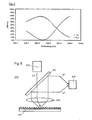
- FIG. 6 indicates the reflection and the transmission as a function of the wavelength. It becomes clear that at no wavelength of the considered range, the reflection approaches 100%. It is very likely that there is a resonant effect, but obviously different from that described in the prior art (Novartis application).
- the FIG. 7 equals to FIG. 6 , where only the wavelength range from 632.8nm to 633.2nm is shown. It can be seen that for a wavelength of 632.95nm the reflection can even be completely suppressed.
- the grating period was not an optimization parameter, since it also depends on diffraction efficiencies and their propagation direction, even of higher diffraction orders. The directions are determined by the grating period. Since these initially play a minor role in the present invention, the grating period is a free parameter that can enter into the optimization accordingly. For this reason, it is possible to adjust the grating, eg by scaling, so that the minimum reflection is at the desired wavelength (633nm in the example). This is particularly advantageous if it must be ensured that no excitation light passes through reflection to the detector for fluorescent light.
- FIG. 8 schematically shows a way how a measurement structure 307 according to the invention can be designed.
- the fluorescence-labeled specific substances coupled on the measuring chip 311 are to be measured.
- the measuring chip 311 is subjected to a substantially parallel excitation light LA at a precisely defined angle. This can be achieved, for example, by transmitting a collimated light beam through a lens 331.
- the excitation light LA comes from a light source 313 and is transmitted through a selective mirror 317 and through the lens 331 and strikes the surface of the measuring chip 311.
- a strong electromagnetic field builds up, which excites the specific substance to be measured and the surface-bound substance to fluoresce.
- Fluorescent light LF then propagates to the lens 331. Since the surface is in the focal plane of the lens 313, this fluorescent light LF propagates as a substantially parallel light beam to the selective mirror 317 which reflects it to a detector 337 which measures the intensity of the fluorescence.
- a light source which simultaneously exposes the lens 331 to different discrete or continuous angles, thus illuminating a plurality of spots or an entire area of the surface of the measuring chip 311.
- a detector row or matrix is used (for example a CCD chip), several areas of the measuring chip can be evaluated at the same time.
- the substances to be measured are applied dissolved in a liquid sample on the substrate. It is important that a small extent of the drops on the surface can be realized. It has been found that, especially with deep trenches, the drops tend to diverge. This is due to the capillary forces acting on the drops through the trenches. In extreme cases, the drops even overlap. To counteract this, the trenches can be blocked by flow barriers. This can be, for example, to the bars transverse, continuous walls. Such walls can be realized by dielectrically coating the platform through a mask. Typical sizes for the diameters of individual measuring fields, referred to below as the spot diameter, are currently 80 ⁇ m to 200 ⁇ m.
- the distance between two walls is at least a factor of three smaller, preferably a factor of five to ten smaller than the spot diameter to be achieved, so that in fact not two drops must share a same intermediate wall area.
- the system according to the invention also allows direct measurement methods, ie measurement methods that do not require specific markers.
- a detailed description of such label-free methods is for example in WO 86/07149 to find.
- the aim of such a measurement can be, for example, the determination of the change in refractive power in a measuring substance which is liquid in the example. This measuring substance fills the trenches of the grid area. If the refractive index in the measuring substance changes, so does the refractive index in the region of the trenches. This change directly affects the configuration of the grid and the field strength distribution that builds up on it.
- This change can be measured by different methods as this has a direct influence on the reflected and / or transmitted diffraction orders (zeroth and higher orders).
- spectral and / or angle-dependent measurements ie measurement of one or more diffraction orders as a function of the wavelength in question.
- Label-free, selective measurement is possible, for example, by specific chemisorption or physisorption, adsorption, desorption and / or chemical bonding (summarized below under the influence of substances) of substances to be measured on the surface.
- This leads to a measurable change in the configuration of the overall distribution of the measuring chip, which determines the field distribution, and in particular that of the grid region.
- a substance effect may change the fill factor of the grating region, which, however, decisively influences the diffraction efficiencies.
- selectivity of such a substance effect can also be achieved by means of an additional layer which specifically binds the substances to be measured on the basis of the so-called key-lock principle. For example, at the beginning of the measurement, only antibodies could be bound to the lattice surface, in particular following the lattice trenches. During the measurement, the corresponding antigens bind and thereby change the lattice configuration.
- the lattice structures so that the lattice trenches are not or only slightly filled, while layer material is deposited substantially on the lattice webs.
- This can be achieved, for example, by coating using sputtering techniques.
- the lattice trench tapers with increasing coating thickness. There is therefore a channel tapering towards the surface, i.
- any desired opening width which is smaller than or equal to the original trench width, can be set. Particles that are in the measurement substance and have a larger diameter than the channel width will not be able to diffuse into the trench region.
- This provides the possibility of integrated mechanical filtering. It is possible to build the tapered channel from a alternating layer system whose material and layer thickness distribution can be optimized with respect to optical requirements.
- a membrane was described, which prefilters the measuring substances and thus causes a preselection. Even with the systems according to the invention such an additional membrane can be connected upstream.
- the system is suitable for the analysis of biological processes that have to do with so-called messengers.
- messengers For example, in some biological processes, penetration of a specific substance on one side of the membrane triggers a specific reaction on the other side of the membrane. This can be, for example, that messengers leave the membrane and diffuse into the adjacent medium. Such messengers can sometimes cause changes in pH. Solutions can be prepared so that such a pH change results in a color change of the solution. The color change is mostly due to a change in the light absorption properties of the solution and such a change in turn has an influence on the field distribution in the grating region, which is measurable according to the invention according to the previously described examples.
- One difficulty may be that the layer system below the grating area interferes with the exposure for making the grating.
- it may be advantageous to switch to an embossing technique in which, for example, a polymer is applied to the layer system, which is then impressed by means of a stamping die a grid. By means of the following lithography, the grating is then transferred to the underlying layer.
- Another way around this difficulty is to choose a system according to the invention, in which the grid is realized in the substrate and transfer the grid structures to the surface.
- Such an embodiment also makes it possible to concentrate according to the invention the essential portion of the electromagnetic field which builds up in the lattice structure and, inter alia, in the lattice trenches accessible for the measuring substances.
- Another aspect of the invention is the possibility that, due to the grid trenches, areas of maximum field strength are accessible to the substances to be measured.
- This inventive aspect can also be achieved by a structured grating region in which one or more of the involved materials has a refractive index which is above the refractive index of the substrate.
Landscapes
- Physics & Mathematics (AREA)
- Chemical & Material Sciences (AREA)
- Health & Medical Sciences (AREA)
- General Physics & Mathematics (AREA)
- Immunology (AREA)
- Analytical Chemistry (AREA)
- Biochemistry (AREA)
- General Health & Medical Sciences (AREA)
- Life Sciences & Earth Sciences (AREA)
- Pathology (AREA)
- Chemical Kinetics & Catalysis (AREA)
- Plasma & Fusion (AREA)
- Engineering & Computer Science (AREA)
- Optics & Photonics (AREA)
- Nuclear Medicine, Radiotherapy & Molecular Imaging (AREA)
- Electrochemistry (AREA)
- Investigating Or Analysing Materials By Optical Means (AREA)
- Secondary Cells (AREA)
- Manufacturing Of Magnetic Record Carriers (AREA)
- Thin Magnetic Films (AREA)
- Investigating Or Analysing Biological Materials (AREA)
- Crystals, And After-Treatments Of Crystals (AREA)
- Particle Accelerators (AREA)
Claims (11)
- Plateforme destinée à produire une répartition de champs électromagnétiques comprenant- un substrat (13)- une couche structurée (19) prévue sur le substrat, l'épaisseur de la couche structurée (19) étant déterminée par la profondeur maximale de la structure,- des moyens d'accouplement (23, 29) destinés à accoupler un rayonnement électromagnétique injecté dans la couche structurée afin d'établir une répartition des champs électromagnétiques à l'intérieur de la couche structurée (19), caractérisée en ce qu'un système multicouches est prévu entre le substrat (13) et la couche structurée (19), de telle sorte que le système multicouches (17) empêche au moins en partie que des champs électromagnétiques, auxquels s'accouplent des ordres de diffraction très élevés, différents de zéro et se propageant dans le substrat (13), soient établis dans la couche structurée (19),la couche structurée (19), les moyens d'accouplement (23, 29) et le système multicouches (17) étant adaptés les uns aux autres de sorte que lorsque la plateforme est soumise de manière appropriée à l'influence d'un rayonnement électromagnétique, l'intensité maximale du champ électromagnétique s'établissant se situe dans la zone de la couche structurée (19).
- Plateforme selon la revendication 1, caractérisée en ce que l'indice de réfraction ou éventuellement l'indice de réfraction effectif de la couche structurée (19) est supérieur de moins de 1%, mais de préférence inférieur à l'indice de réfraction du substrat (13).
- Plateforme selon l'une quelconque des revendications 1 et 2, caractérisée en ce que la structure de la couche structurée (19) comporte des formations en creux (29) disposées de façon sensiblement périodique qui font partie des moyens d'accouplement.
- Plateforme selon l'une quelconque des revendications précédentes, caractérisée en ce que le système multicouches (17) comporte des couches métalliques composées de préférence de Al et/ou de Ag.
- Plateforme selon l'une quelconque des revendications 1 à 3, caractérisée en ce que le système multicouches (17) comporte des couches diélectrique et ne comporte de préférence aucune couche métallique, le système multicouches présentant de préférence une construction de couches alternées dans laquelle les couches présentant un haut indice de réfraction et un faible indice de réfraction sont disposées en alternance.
- Plateforme selon les revendications 1 à 5, caractérisée en ce que le type de structuration, les moyens d'accouplement (23, 29) et le nombre ainsi que le matériau et la répartition d'épaisseur des couches du système multicouches sont sélectionnés de sorte que lorsque la plateforme est soumise à l'influence appropriée d'un rayonnement électromagnétique, la répartition des champs électromagnétiques s'établissant comprend au moins un maximum dans les zones exemptes de matériau de couche (29) de la couche structurée (19).
- Plateforme de répartition des champs comportant une plateforme selon l'une quelconque des revendications 1 à 6, comprenant une source pour la production d'un rayonnement électromagnétique et comprenant un champ électromagnétique dont l'intensité est maximale dans la zone de la couche structurée.
- Plateforme de répartition des champs comportant une plateforme selon l'une quelconque des revendications 1 à 7, caractérisée en ce que la répartition des champs électromagnétiques comprend au moins un maximum dans la zone exempte de matériau de couche (29) de la couche structurée (19).
- Capteur comprenant une plateforme ou une plateforme de répartition des champs selon l'une quelconque des revendication précédentes destinée à mesurer des substances spécifiques dans un échantillon biologique et/ou chimique et/ou biochimique.
- Procédé de production d'une répartition excessive, non exclusivement évanescente de champs électromagnétiques, comprenant les étapes suivantes consistant à :- sélectionner un substrat (13)- sélectionner le matériau et la structure d'une couche structurée- sélectionner les matériaux pour un système multicouches- déterminer les paramètres d'un rayonnement électromagnétique à utiliser pour l'injection- simuler et optimiser la répartition des champs électromagnétiques à l'intérieur d'une plateforme comportant le substrat, le système multicouches et la couche structurée lorsqu'elle est soumise à l'influence d'un rayonnement électromagnétique selon les paramètres déterminés, le système multicouches étant prévu entre le substrat et la couche structurée et devant au moins en partie empêcher que des champs électromagnétiques auxquels s'accouplent des ordres de diffraction des champs très élevés, différents de zéro et se propageant dans le substrat (13) soient établis dans la couche structurée (19) et que l'intensité maximale des champs en un point situé à l'intérieur de la couche structurée soit définie comme objectif d'optimisation ;- concevoir la plateforme au moins approximativement selon le résultat de l'optimisation ;- soumettre la plateforme à l'influence d'un rayonnement électromagnétique selon les paramètres déterminés.
- Procédé selon la revendication 10, caractérisé en ce qu'on cherche à obtenir, comme objectif d'optimisation à poursuivre, une répartition électromagnétique des champs comprenant au moins un maximum dans les zones exemptes de matériau de couche de la couche structurée.
Applications Claiming Priority (3)
| Application Number | Priority Date | Filing Date | Title |
|---|---|---|---|
| US43498702P | 2002-12-19 | 2002-12-19 | |
| US434987P | 2002-12-19 | ||
| PCT/CH2003/000811 WO2004057315A1 (fr) | 2002-12-19 | 2003-12-11 | Procede pour creer des repartitions de champs electromagnetiques |
Publications (2)
| Publication Number | Publication Date |
|---|---|
| EP1576356A1 EP1576356A1 (fr) | 2005-09-21 |
| EP1576356B1 true EP1576356B1 (fr) | 2009-10-28 |
Family
ID=32682135
Family Applications (1)
| Application Number | Title | Priority Date | Filing Date |
|---|---|---|---|
| EP03775037A Expired - Lifetime EP1576356B1 (fr) | 2002-12-19 | 2003-12-11 | Appareil et procede pour creer des repartitions de champs electromagnetiques |
Country Status (9)
| Country | Link |
|---|---|
| US (1) | US7110181B2 (fr) |
| EP (1) | EP1576356B1 (fr) |
| KR (1) | KR20050084016A (fr) |
| CN (1) | CN100585384C (fr) |
| AT (1) | ATE447171T1 (fr) |
| AU (1) | AU2003283175A1 (fr) |
| DE (1) | DE50312077D1 (fr) |
| TW (1) | TWI322264B (fr) |
| WO (1) | WO2004057315A1 (fr) |
Families Citing this family (51)
| Publication number | Priority date | Publication date | Assignee | Title |
|---|---|---|---|---|
| US6380751B2 (en) | 1992-06-11 | 2002-04-30 | Cascade Microtech, Inc. | Wafer probe station having environment control enclosure |
| US5345170A (en) | 1992-06-11 | 1994-09-06 | Cascade Microtech, Inc. | Wafer probe station having integrated guarding, Kelvin connection and shielding systems |
| US5561377A (en) | 1995-04-14 | 1996-10-01 | Cascade Microtech, Inc. | System for evaluating probing networks |
| US6232789B1 (en) | 1997-05-28 | 2001-05-15 | Cascade Microtech, Inc. | Probe holder for low current measurements |
| US5914613A (en) | 1996-08-08 | 1999-06-22 | Cascade Microtech, Inc. | Membrane probing system with local contact scrub |
| US6002263A (en) | 1997-06-06 | 1999-12-14 | Cascade Microtech, Inc. | Probe station having inner and outer shielding |
| US6256882B1 (en) | 1998-07-14 | 2001-07-10 | Cascade Microtech, Inc. | Membrane probing system |
| US6578264B1 (en) | 1999-06-04 | 2003-06-17 | Cascade Microtech, Inc. | Method for constructing a membrane probe using a depression |
| US6445202B1 (en) | 1999-06-30 | 2002-09-03 | Cascade Microtech, Inc. | Probe station thermal chuck with shielding for capacitive current |
| US6838890B2 (en) | 2000-02-25 | 2005-01-04 | Cascade Microtech, Inc. | Membrane probing system |
| US6965226B2 (en) | 2000-09-05 | 2005-11-15 | Cascade Microtech, Inc. | Chuck for holding a device under test |
| US6914423B2 (en) | 2000-09-05 | 2005-07-05 | Cascade Microtech, Inc. | Probe station |
| DE10143173A1 (de) | 2000-12-04 | 2002-06-06 | Cascade Microtech Inc | Wafersonde |
| US7355420B2 (en) | 2001-08-21 | 2008-04-08 | Cascade Microtech, Inc. | Membrane probing system |
| US6777964B2 (en) | 2002-01-25 | 2004-08-17 | Cascade Microtech, Inc. | Probe station |
| EP1509776A4 (fr) | 2002-05-23 | 2010-08-18 | Cascade Microtech Inc | Sonde d'essai d'un dispositif soumis essai |
| US7863052B2 (en) * | 2005-08-11 | 2011-01-04 | Sru Biosystems, Inc. | Grating-based sensor combining label-free binding detection and fluorescence amplification and readout system for sensor |
| US6847219B1 (en) | 2002-11-08 | 2005-01-25 | Cascade Microtech, Inc. | Probe station with low noise characteristics |
| US6724205B1 (en) | 2002-11-13 | 2004-04-20 | Cascade Microtech, Inc. | Probe for combined signals |
| US7250779B2 (en) | 2002-11-25 | 2007-07-31 | Cascade Microtech, Inc. | Probe station with low inductance path |
| US6861856B2 (en) | 2002-12-13 | 2005-03-01 | Cascade Microtech, Inc. | Guarded tub enclosure |
| US7221172B2 (en) | 2003-05-06 | 2007-05-22 | Cascade Microtech, Inc. | Switched suspended conductor and connection |
| US7057404B2 (en) | 2003-05-23 | 2006-06-06 | Sharp Laboratories Of America, Inc. | Shielded probe for testing a device under test |
| US7492172B2 (en) | 2003-05-23 | 2009-02-17 | Cascade Microtech, Inc. | Chuck for holding a device under test |
| US7250626B2 (en) | 2003-10-22 | 2007-07-31 | Cascade Microtech, Inc. | Probe testing structure |
| US7187188B2 (en) | 2003-12-24 | 2007-03-06 | Cascade Microtech, Inc. | Chuck with integrated wafer support |
| WO2005065258A2 (fr) | 2003-12-24 | 2005-07-21 | Cascade Microtech, Inc. | Sonde de tranche a semi-conducteur possedant un circuit actif |
| DE202005021434U1 (de) | 2004-06-07 | 2008-03-20 | Cascade Microtech, Inc., Beaverton | Thermooptische Einspannvorrichtung |
| US7330041B2 (en) | 2004-06-14 | 2008-02-12 | Cascade Microtech, Inc. | Localizing a temperature of a device for testing |
| KR101157449B1 (ko) | 2004-07-07 | 2012-06-22 | 캐스케이드 마이크로테크 인코포레이티드 | 멤브레인 서스펜디드 프로브를 구비한 프로브 헤드 |
| KR20070058522A (ko) | 2004-09-13 | 2007-06-08 | 캐스케이드 마이크로테크 인코포레이티드 | 양측 프루빙 구조 |
| US7535247B2 (en) | 2005-01-31 | 2009-05-19 | Cascade Microtech, Inc. | Interface for testing semiconductors |
| US7656172B2 (en) | 2005-01-31 | 2010-02-02 | Cascade Microtech, Inc. | System for testing semiconductors |
| US7449899B2 (en) | 2005-06-08 | 2008-11-11 | Cascade Microtech, Inc. | Probe for high frequency signals |
| EP1932003A2 (fr) | 2005-06-13 | 2008-06-18 | Cascade Microtech, Inc. | Sonde de signal differentiel active-passive a large bande |
| US7790406B2 (en) * | 2005-08-11 | 2010-09-07 | Sru Biosystems, Inc | Grating-based sensor combining label-free binding detection and fluorescence amplification and readout system for sensor |
| US7609077B2 (en) | 2006-06-09 | 2009-10-27 | Cascade Microtech, Inc. | Differential signal probe with integral balun |
| US7723999B2 (en) | 2006-06-12 | 2010-05-25 | Cascade Microtech, Inc. | Calibration structures for differential signal probing |
| US7764072B2 (en) | 2006-06-12 | 2010-07-27 | Cascade Microtech, Inc. | Differential signal probing system |
| US7443186B2 (en) | 2006-06-12 | 2008-10-28 | Cascade Microtech, Inc. | On-wafer test structures for differential signals |
| US7403028B2 (en) | 2006-06-12 | 2008-07-22 | Cascade Microtech, Inc. | Test structure and probe for differential signals |
| US20080012578A1 (en) * | 2006-07-14 | 2008-01-17 | Cascade Microtech, Inc. | System for detecting molecular structure and events |
| WO2008010182A2 (fr) * | 2006-07-17 | 2008-01-24 | Max Wiki | Système analytique présentant un dispositif de modulation de la lumière dans l'espace et variant en fonction du temps, et procédé d'identification mis en oeuvre au moyen de ce système |
| US7876114B2 (en) | 2007-08-08 | 2011-01-25 | Cascade Microtech, Inc. | Differential waveguide probe |
| EP2060904A1 (fr) * | 2007-11-13 | 2009-05-20 | Koninklijke Philips Electronics N.V. | Biocapteur de réseau à plasmon |
| US7888957B2 (en) | 2008-10-06 | 2011-02-15 | Cascade Microtech, Inc. | Probing apparatus with impedance optimized interface |
| US8410806B2 (en) | 2008-11-21 | 2013-04-02 | Cascade Microtech, Inc. | Replaceable coupon for a probing apparatus |
| US8319503B2 (en) | 2008-11-24 | 2012-11-27 | Cascade Microtech, Inc. | Test apparatus for measuring a characteristic of a device under test |
| EP2221605A1 (fr) * | 2009-02-12 | 2010-08-25 | Koninklijke Philips Electronics N.V. | Capteur de treillis |
| FR2954524B1 (fr) * | 2009-12-17 | 2012-09-28 | Ecole Polytech | Reseau de diffraction reflechissant dielectrique optimise |
| TWI571648B (zh) * | 2016-01-26 | 2017-02-21 | 國立彰化師範大學 | 磁場分佈感測系統 |
Family Cites Families (6)
| Publication number | Priority date | Publication date | Assignee | Title |
|---|---|---|---|---|
| GB2256477B (en) * | 1991-06-07 | 1995-03-08 | Marconi Gec Ltd | An optical sensor |
| US5907436A (en) * | 1995-09-29 | 1999-05-25 | The Regents Of The University Of California | Multilayer dielectric diffraction gratings |
| EP0920696B1 (fr) * | 1996-08-21 | 2003-05-14 | Polaroid Corporation | Systemes et methodes utilisant les champs evanescents a commande de phase |
| GB9803704D0 (en) * | 1998-02-24 | 1998-04-15 | Univ Manchester | Waveguide structure |
| WO2001079821A1 (fr) * | 2000-04-14 | 2001-10-25 | Zeptosens Ag | Structure reseau de guide d'onde destine a intensifier un champ d'excitation et son utilisation |
| AU2001281743A1 (en) * | 2000-07-21 | 2002-02-05 | Micro Managed Photons A/S | Surface plasmon polariton band gap structures |
-
2003
- 2003-12-11 AT AT03775037T patent/ATE447171T1/de not_active IP Right Cessation
- 2003-12-11 KR KR1020057009647A patent/KR20050084016A/ko not_active Withdrawn
- 2003-12-11 DE DE50312077T patent/DE50312077D1/de not_active Expired - Lifetime
- 2003-12-11 AU AU2003283175A patent/AU2003283175A1/en not_active Abandoned
- 2003-12-11 CN CN200380107136A patent/CN100585384C/zh not_active Expired - Fee Related
- 2003-12-11 WO PCT/CH2003/000811 patent/WO2004057315A1/fr not_active Ceased
- 2003-12-11 EP EP03775037A patent/EP1576356B1/fr not_active Expired - Lifetime
- 2003-12-18 US US10/740,057 patent/US7110181B2/en not_active Expired - Fee Related
- 2003-12-18 TW TW092135937A patent/TWI322264B/zh not_active IP Right Cessation
Also Published As
| Publication number | Publication date |
|---|---|
| DE50312077D1 (de) | 2009-12-10 |
| US20040130787A1 (en) | 2004-07-08 |
| CN1729393A (zh) | 2006-02-01 |
| KR20050084016A (ko) | 2005-08-26 |
| EP1576356A1 (fr) | 2005-09-21 |
| WO2004057315A1 (fr) | 2004-07-08 |
| TW200420876A (en) | 2004-10-16 |
| ATE447171T1 (de) | 2009-11-15 |
| AU2003283175A1 (en) | 2004-07-14 |
| CN100585384C (zh) | 2010-01-27 |
| US7110181B2 (en) | 2006-09-19 |
| TWI322264B (en) | 2010-03-21 |
Similar Documents
| Publication | Publication Date | Title |
|---|---|---|
| EP1576356B1 (fr) | Appareil et procede pour creer des repartitions de champs electromagnetiques | |
| DE69531125T2 (de) | Nachweis einer Zielsubstanz in einer Probe | |
| DE19544125B4 (de) | Verfahren zur Herstellung eines Beugungsgitters, Lichtleiterbauteil sowie deren Verwendungen | |
| EP0455067B1 (fr) | Capteur microoptique | |
| DE69527390T2 (de) | Vorrichtung und Verfahren zur intrakavitären Messung der makroskopischen Eigenschaften von Chemikalien | |
| EP0618441B1 (fr) | Dispositif pour examiner par résolution latérale une couche ultra-mince à hétérogénéité latérale | |
| EP1250618A1 (fr) | Procede de realisation d'une structure reticulaire, element optique, plaque de detection a champ evanescent, plaque a microtitration, coupleur optique utilise dans la technique de communication, et dispositif pour surveiller une longueur d'onde | |
| DE102009035578B3 (de) | Faseroptischer Oberflächenplasmonen-Resonanz-Sensor zur Bestimmung von Brechzahlen faserangrenzender Medien | |
| EP1190236A1 (fr) | Plate-forme de capteurs et procede permettant de determiner plusieurs substances a analyser | |
| EP1443320A2 (fr) | Puce de détecteur pour caractériser une substance chimique et/ou biochimique | |
| EP1769246A1 (fr) | Systeme analytique et procede pour analyser des signaux optiques non lineaires | |
| EP3201606B1 (fr) | Dispositif et procédé de détermination d'un indice de réfraction | |
| EP1272829A1 (fr) | Structure reseau de guide d'onde destine a intensifier un champ d'excitation et son utilisation | |
| WO2001069256A2 (fr) | Element capteur pour la detection optique d'analytes chimiques ou biochimiques | |
| DE102014104595A1 (de) | Verfahren und Vorrichtung zur labelfreien Detektion eines Analyten | |
| DE102016206088A1 (de) | Verfahren zum Bestimmen der Dicke einer kontaminierenden Schicht und/oder der Art eines kontaminierenden Materials, optisches Element und EUV-Lithographiesystem | |
| DE10006083B4 (de) | Verfahren zur quantitativen und/oder qualitativen Bestimmung von Schichtdicken sowie ein Mikroreaktionsgefäß und eine Titerplatte | |
| DE102013108584B3 (de) | Substrat für die Erzeugung von Oberflächenplasmonen und Oberflächenpolaritonen mittels einer Anregungsstrahlung, Verfahren zur Herstellung des Substrats und Verwendungen des Substrats | |
| EP1222029A1 (fr) | Substrat comportant au moins un pore | |
| EP1644721B1 (fr) | Systeme de capteurs | |
| WO2022238313A1 (fr) | Capteur de bragg à fibre destiné à détecter une substance cible et procédé de fabrication d'un capteur de bragg à fibre pour détecter une substance cible | |
| DE102015218422A1 (de) | Sensorelement für Photolumineszenz-Messungen, Photolumineszenz-Detektionseinrichtung, Verfahren zum Betreiben einer Photolumineszenz-Detektionseinrichtung, Verfahren zur Herstellung eines Sensorelements, und Verwendung eines Sensorelements | |
| DE102004015906B4 (de) | Mikrofluidische Vorrichtung für die optische Analyse | |
| DE102005015030A1 (de) | Verfahren zur Untersuchung physikalischer, chemischer und biochemischer Wechselwirkungen | |
| WO2006008112A1 (fr) | Dispositif d'ellipsometrie a plate-forme de resonance |
Legal Events
| Date | Code | Title | Description |
|---|---|---|---|
| PUAI | Public reference made under article 153(3) epc to a published international application that has entered the european phase |
Free format text: ORIGINAL CODE: 0009012 |
|
| 17P | Request for examination filed |
Effective date: 20050719 |
|
| AK | Designated contracting states |
Kind code of ref document: A1 Designated state(s): AT BE BG CH CY CZ DE DK EE ES FI FR GB GR HU IE IT LI LU MC NL PT RO SE SI SK TR |
|
| AX | Request for extension of the european patent |
Extension state: AL LT LV MK |
|
| DAX | Request for extension of the european patent (deleted) | ||
| RAP1 | Party data changed (applicant data changed or rights of an application transferred) |
Owner name: OC OERLIKON BALZERS AG |
|
| RIN1 | Information on inventor provided before grant (corrected) |
Inventor name: HEINE-KEMPKENS, CLAUS Inventor name: THOME-FOERSTER, HEIDI |
|
| 17Q | First examination report despatched |
Effective date: 20070209 |
|
| RAP1 | Party data changed (applicant data changed or rights of an application transferred) |
Owner name: OERLIKON TRADING AG, TRUEBBACH |
|
| GRAP | Despatch of communication of intention to grant a patent |
Free format text: ORIGINAL CODE: EPIDOSNIGR1 |
|
| RTI1 | Title (correction) |
Free format text: APPARATUS AND METHOD FOR GENERATING ELECTROMAGNETIC FIELD DISTRIBUTIONS |
|
| GRAS | Grant fee paid |
Free format text: ORIGINAL CODE: EPIDOSNIGR3 |
|
| GRAA | (expected) grant |
Free format text: ORIGINAL CODE: 0009210 |
|
| AK | Designated contracting states |
Kind code of ref document: B1 Designated state(s): AT BE BG CH CY CZ DE DK EE ES FI FR GB GR HU IE IT LI LU MC NL PT RO SE SI SK TR |
|
| REG | Reference to a national code |
Ref country code: GB Ref legal event code: FG4D Free format text: NOT ENGLISH |
|
| REG | Reference to a national code |
Ref country code: CH Ref legal event code: EP |
|
| REG | Reference to a national code |
Ref country code: IE Ref legal event code: FG4D |
|
| REF | Corresponds to: |
Ref document number: 50312077 Country of ref document: DE Date of ref document: 20091210 Kind code of ref document: P |
|
| NLV1 | Nl: lapsed or annulled due to failure to fulfill the requirements of art. 29p and 29m of the patents act | ||
| PG25 | Lapsed in a contracting state [announced via postgrant information from national office to epo] |
Ref country code: ES Free format text: LAPSE BECAUSE OF FAILURE TO SUBMIT A TRANSLATION OF THE DESCRIPTION OR TO PAY THE FEE WITHIN THE PRESCRIBED TIME-LIMIT Effective date: 20100208 Ref country code: PT Free format text: LAPSE BECAUSE OF FAILURE TO SUBMIT A TRANSLATION OF THE DESCRIPTION OR TO PAY THE FEE WITHIN THE PRESCRIBED TIME-LIMIT Effective date: 20100301 Ref country code: SE Free format text: LAPSE BECAUSE OF FAILURE TO SUBMIT A TRANSLATION OF THE DESCRIPTION OR TO PAY THE FEE WITHIN THE PRESCRIBED TIME-LIMIT Effective date: 20091028 Ref country code: FI Free format text: LAPSE BECAUSE OF FAILURE TO SUBMIT A TRANSLATION OF THE DESCRIPTION OR TO PAY THE FEE WITHIN THE PRESCRIBED TIME-LIMIT Effective date: 20091028 |
|
| REG | Reference to a national code |
Ref country code: IE Ref legal event code: FD4D |
|
| PG25 | Lapsed in a contracting state [announced via postgrant information from national office to epo] |
Ref country code: CY Free format text: LAPSE BECAUSE OF FAILURE TO SUBMIT A TRANSLATION OF THE DESCRIPTION OR TO PAY THE FEE WITHIN THE PRESCRIBED TIME-LIMIT Effective date: 20091028 Ref country code: SI Free format text: LAPSE BECAUSE OF FAILURE TO SUBMIT A TRANSLATION OF THE DESCRIPTION OR TO PAY THE FEE WITHIN THE PRESCRIBED TIME-LIMIT Effective date: 20091028 |
|
| BERE | Be: lapsed |
Owner name: OERLIKON TRADING AG, TRUBBACH Effective date: 20091231 |
|
| PG25 | Lapsed in a contracting state [announced via postgrant information from national office to epo] |
Ref country code: EE Free format text: LAPSE BECAUSE OF FAILURE TO SUBMIT A TRANSLATION OF THE DESCRIPTION OR TO PAY THE FEE WITHIN THE PRESCRIBED TIME-LIMIT Effective date: 20091028 Ref country code: MC Free format text: LAPSE BECAUSE OF NON-PAYMENT OF DUE FEES Effective date: 20100701 Ref country code: BG Free format text: LAPSE BECAUSE OF FAILURE TO SUBMIT A TRANSLATION OF THE DESCRIPTION OR TO PAY THE FEE WITHIN THE PRESCRIBED TIME-LIMIT Effective date: 20100128 Ref country code: RO Free format text: LAPSE BECAUSE OF FAILURE TO SUBMIT A TRANSLATION OF THE DESCRIPTION OR TO PAY THE FEE WITHIN THE PRESCRIBED TIME-LIMIT Effective date: 20091028 Ref country code: IE Free format text: LAPSE BECAUSE OF FAILURE TO SUBMIT A TRANSLATION OF THE DESCRIPTION OR TO PAY THE FEE WITHIN THE PRESCRIBED TIME-LIMIT Effective date: 20091028 Ref country code: DK Free format text: LAPSE BECAUSE OF FAILURE TO SUBMIT A TRANSLATION OF THE DESCRIPTION OR TO PAY THE FEE WITHIN THE PRESCRIBED TIME-LIMIT Effective date: 20091028 |
|
| PG25 | Lapsed in a contracting state [announced via postgrant information from national office to epo] |
Ref country code: SK Free format text: LAPSE BECAUSE OF FAILURE TO SUBMIT A TRANSLATION OF THE DESCRIPTION OR TO PAY THE FEE WITHIN THE PRESCRIBED TIME-LIMIT Effective date: 20091028 Ref country code: CZ Free format text: LAPSE BECAUSE OF FAILURE TO SUBMIT A TRANSLATION OF THE DESCRIPTION OR TO PAY THE FEE WITHIN THE PRESCRIBED TIME-LIMIT Effective date: 20091028 |
|
| PLBE | No opposition filed within time limit |
Free format text: ORIGINAL CODE: 0009261 |
|
| STAA | Information on the status of an ep patent application or granted ep patent |
Free format text: STATUS: NO OPPOSITION FILED WITHIN TIME LIMIT |
|
| 26N | No opposition filed |
Effective date: 20100729 |
|
| PG25 | Lapsed in a contracting state [announced via postgrant information from national office to epo] |
Ref country code: GR Free format text: LAPSE BECAUSE OF FAILURE TO SUBMIT A TRANSLATION OF THE DESCRIPTION OR TO PAY THE FEE WITHIN THE PRESCRIBED TIME-LIMIT Effective date: 20100129 Ref country code: BE Free format text: LAPSE BECAUSE OF NON-PAYMENT OF DUE FEES Effective date: 20091231 |
|
| PG25 | Lapsed in a contracting state [announced via postgrant information from national office to epo] |
Ref country code: IT Free format text: LAPSE BECAUSE OF FAILURE TO SUBMIT A TRANSLATION OF THE DESCRIPTION OR TO PAY THE FEE WITHIN THE PRESCRIBED TIME-LIMIT Effective date: 20091028 |
|
| PG25 | Lapsed in a contracting state [announced via postgrant information from national office to epo] |
Ref country code: LU Free format text: LAPSE BECAUSE OF NON-PAYMENT OF DUE FEES Effective date: 20091211 |
|
| PG25 | Lapsed in a contracting state [announced via postgrant information from national office to epo] |
Ref country code: AT Free format text: LAPSE BECAUSE OF NON-PAYMENT OF DUE FEES Effective date: 20091211 |
|
| PG25 | Lapsed in a contracting state [announced via postgrant information from national office to epo] |
Ref country code: HU Free format text: LAPSE BECAUSE OF FAILURE TO SUBMIT A TRANSLATION OF THE DESCRIPTION OR TO PAY THE FEE WITHIN THE PRESCRIBED TIME-LIMIT Effective date: 20100429 |
|
| PG25 | Lapsed in a contracting state [announced via postgrant information from national office to epo] |
Ref country code: TR Free format text: LAPSE BECAUSE OF FAILURE TO SUBMIT A TRANSLATION OF THE DESCRIPTION OR TO PAY THE FEE WITHIN THE PRESCRIBED TIME-LIMIT Effective date: 20091028 |
|
| PG25 | Lapsed in a contracting state [announced via postgrant information from national office to epo] |
Ref country code: NL Free format text: LAPSE BECAUSE OF FAILURE TO SUBMIT A TRANSLATION OF THE DESCRIPTION OR TO PAY THE FEE WITHIN THE PRESCRIBED TIME-LIMIT Effective date: 20091028 |
|
| REG | Reference to a national code |
Ref country code: FR Ref legal event code: PLFP Year of fee payment: 13 |
|
| PGFP | Annual fee paid to national office [announced via postgrant information from national office to epo] |
Ref country code: DE Payment date: 20151208 Year of fee payment: 13 Ref country code: GB Payment date: 20151209 Year of fee payment: 13 |
|
| PGFP | Annual fee paid to national office [announced via postgrant information from national office to epo] |
Ref country code: FR Payment date: 20151110 Year of fee payment: 13 |
|
| PGFP | Annual fee paid to national office [announced via postgrant information from national office to epo] |
Ref country code: CH Payment date: 20160324 Year of fee payment: 13 |
|
| REG | Reference to a national code |
Ref country code: DE Ref legal event code: R119 Ref document number: 50312077 Country of ref document: DE |
|
| REG | Reference to a national code |
Ref country code: CH Ref legal event code: PL |
|
| GBPC | Gb: european patent ceased through non-payment of renewal fee |
Effective date: 20161211 |
|
| REG | Reference to a national code |
Ref country code: FR Ref legal event code: ST Effective date: 20170831 |
|
| PG25 | Lapsed in a contracting state [announced via postgrant information from national office to epo] |
Ref country code: CH Free format text: LAPSE BECAUSE OF NON-PAYMENT OF DUE FEES Effective date: 20161231 Ref country code: LI Free format text: LAPSE BECAUSE OF NON-PAYMENT OF DUE FEES Effective date: 20161231 Ref country code: FR Free format text: LAPSE BECAUSE OF NON-PAYMENT OF DUE FEES Effective date: 20170102 |
|
| PG25 | Lapsed in a contracting state [announced via postgrant information from national office to epo] |
Ref country code: DE Free format text: LAPSE BECAUSE OF NON-PAYMENT OF DUE FEES Effective date: 20170701 Ref country code: GB Free format text: LAPSE BECAUSE OF NON-PAYMENT OF DUE FEES Effective date: 20161211 |