EP1577875A1 - Commande de dispositif d'affichage electrochromique - Google Patents
Commande de dispositif d'affichage electrochromique Download PDFInfo
- Publication number
- EP1577875A1 EP1577875A1 EP04015547A EP04015547A EP1577875A1 EP 1577875 A1 EP1577875 A1 EP 1577875A1 EP 04015547 A EP04015547 A EP 04015547A EP 04015547 A EP04015547 A EP 04015547A EP 1577875 A1 EP1577875 A1 EP 1577875A1
- Authority
- EP
- European Patent Office
- Prior art keywords
- voltage
- pixels
- pixel
- electrochromic
- activation
- Prior art date
- Legal status (The legal status is an assumption and is not a legal conclusion. Google has not performed a legal analysis and makes no representation as to the accuracy of the status listed.)
- Withdrawn
Links
- 230000004913 activation Effects 0.000 claims abstract description 17
- 238000000034 method Methods 0.000 claims abstract description 13
- 238000004043 dyeing Methods 0.000 claims description 4
- 238000004040 coloring Methods 0.000 claims description 3
- 239000000463 material Substances 0.000 abstract description 10
- 239000000126 substance Substances 0.000 abstract description 5
- 230000001419 dependent effect Effects 0.000 abstract description 3
- 230000020411 cell activation Effects 0.000 abstract 1
- 238000002845 discoloration Methods 0.000 description 8
- 239000011159 matrix material Substances 0.000 description 5
- 238000010586 diagram Methods 0.000 description 4
- 239000003990 capacitor Substances 0.000 description 3
- 241001136792 Alle Species 0.000 description 2
- 238000012217 deletion Methods 0.000 description 2
- 230000037430 deletion Effects 0.000 description 2
- 230000003647 oxidation Effects 0.000 description 2
- 238000007254 oxidation reaction Methods 0.000 description 2
- 230000032683 aging Effects 0.000 description 1
- 238000010276 construction Methods 0.000 description 1
- 238000004042 decolorization Methods 0.000 description 1
- 230000018109 developmental process Effects 0.000 description 1
- 238000007599 discharging Methods 0.000 description 1
- 230000005611 electricity Effects 0.000 description 1
- 230000007774 longterm Effects 0.000 description 1
- 238000009877 rendering Methods 0.000 description 1
Images
Classifications
-
- G—PHYSICS
- G09—EDUCATION; CRYPTOGRAPHY; DISPLAY; ADVERTISING; SEALS
- G09G—ARRANGEMENTS OR CIRCUITS FOR CONTROL OF INDICATING DEVICES USING STATIC MEANS TO PRESENT VARIABLE INFORMATION
- G09G3/00—Control arrangements or circuits, of interest only in connection with visual indicators other than cathode-ray tubes
- G09G3/20—Control arrangements or circuits, of interest only in connection with visual indicators other than cathode-ray tubes for presentation of an assembly of a number of characters, e.g. a page, by composing the assembly by combination of individual elements arranged in a matrix no fixed position being assigned to or needed to be assigned to the individual characters or partial characters
- G09G3/34—Control arrangements or circuits, of interest only in connection with visual indicators other than cathode-ray tubes for presentation of an assembly of a number of characters, e.g. a page, by composing the assembly by combination of individual elements arranged in a matrix no fixed position being assigned to or needed to be assigned to the individual characters or partial characters by control of light from an independent source
- G09G3/38—Control arrangements or circuits, of interest only in connection with visual indicators other than cathode-ray tubes for presentation of an assembly of a number of characters, e.g. a page, by composing the assembly by combination of individual elements arranged in a matrix no fixed position being assigned to or needed to be assigned to the individual characters or partial characters by control of light from an independent source using electrochromic devices
-
- G—PHYSICS
- G09—EDUCATION; CRYPTOGRAPHY; DISPLAY; ADVERTISING; SEALS
- G09G—ARRANGEMENTS OR CIRCUITS FOR CONTROL OF INDICATING DEVICES USING STATIC MEANS TO PRESENT VARIABLE INFORMATION
- G09G2310/00—Command of the display device
- G09G2310/02—Addressing, scanning or driving the display screen or processing steps related thereto
- G09G2310/0243—Details of the generation of driving signals
- G09G2310/0251—Precharge or discharge of pixel before applying new pixel voltage
-
- G—PHYSICS
- G09—EDUCATION; CRYPTOGRAPHY; DISPLAY; ADVERTISING; SEALS
- G09G—ARRANGEMENTS OR CIRCUITS FOR CONTROL OF INDICATING DEVICES USING STATIC MEANS TO PRESENT VARIABLE INFORMATION
- G09G2310/00—Command of the display device
- G09G2310/02—Addressing, scanning or driving the display screen or processing steps related thereto
- G09G2310/0243—Details of the generation of driving signals
- G09G2310/0254—Control of polarity reversal in general, other than for liquid crystal displays
-
- G—PHYSICS
- G09—EDUCATION; CRYPTOGRAPHY; DISPLAY; ADVERTISING; SEALS
- G09G—ARRANGEMENTS OR CIRCUITS FOR CONTROL OF INDICATING DEVICES USING STATIC MEANS TO PRESENT VARIABLE INFORMATION
- G09G2310/00—Command of the display device
- G09G2310/06—Details of flat display driving waveforms
- G09G2310/061—Details of flat display driving waveforms for resetting or blanking
Definitions
- the invention relates to a method for pixel-individual Dyeing and / or discoloring in one of electrochromic pixels constructed display device.
- Such electrochromic pixels or cells are based on the chemical oxidation or reduction of electrochromic materials, depending on their chemical state change their color.
- the oxidation or reduction can be controlled by a current flow through the cell, the color change being similar to loading or unloading a capacitor takes place.
- the control of the pixels in the display device takes place for example, by a passive matrix drive, wherein the electrochromic material is between two electrodes.
- the (passive matrix) control loses the electrochromic Material in the times when the pixels are not be controlled, something in the previously achieved discoloration and it thus lengthens the time until a desired Degree of discoloration is achieved.
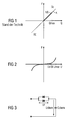
- FIG. 1 is for explanation a discoloration charge diagram electrochromic cells or pixels.
- the self-explanatory diagram shows a k-line K for the Dependence of a color F of the pixel on the stored Charge Q.
- the electrochromic material is in one Passive matrix between a viewing electrode SE and a return electrode RE arranged, wherein the electrodes SE RE the of the polarity of the stored charge Q dependent color F exhibit.
- Currently used color combinations are yellow-blue, yellow-red or blue to white.
- electrochromic cells are metastable, i. the last one reached state is maintained over a longer period.
- Within the charge range of a cell is only one certain area NB usable by the zero line and a maximum value Qmax is determined for the charge Q.
- the invention is based on the object described above To eliminate problems.
- the inventive method allows a considerable faster image rendering because the pixels are not from scratch to be loaded.
- the charge state of each pixel or Image pixels are no longer monitored. from that result in lower processing power and a lower one Memory requirements. Next, there is no zero drift anymore instead of.
- a discoloration / voltage characteristic typical of electrochromic cells is shown in FIG.
- a high Contrast range can be used as a limitation of the working characteristic or a workspace practically the zero point on one side and a voltage Umax on the other Page to be selected. By the charge quantity differences between these two values becomes a high metastability reached.
- this is analogous to the voltage range be understood on the working characteristic, the between a state of the pixel with displayed content, respectively Color and a condition without content lies.
- Voltage Ue is just below an activation voltage Uf, by the materials used and chemical potentials Uchem (see FIG. 3) of an electrochromic Cell is dependent.
- the usable contrast range it reduces slightly and the necessary amount of charge Switching significantly reduces.
- FIG. 3 is a simplified electrical Equivalent circuit diagram indicated. It is assumed that the pixel is approximated by two antiparallel diodes be described with a downstream capacitor Cchem can. At the unspecified diodes falls the Activation voltage Uf (see also Figure 2) from, and on the Capacitor Cchem a charging voltage Uchem.
- Pixel may be a display or a display device being constructed.
- the drive voltage must be or driving time for a new image the current Consider image information.
- the control writes per Pixel thereby the difference of contents to be displayed and straight displayed content or stored cargo.
- the pixels or cells with a bias voltage Ue corresponds to the voltage value Ue in FIG 2) with a value just below the activation voltage Uf permanently driven.
- the bias voltage Ue has a negative sign relative to the charge contained in the cell.
- the decolorization or deletion of a pixel happens by deprivation of charge. This is one in the cell stored charge Q opposite voltage applied. Again, this must be stored in the pixel before discoloring Charge Q be known.
- a crosstalk between the pixels, the temperature, the materials used and their aging has a dynamic influence on the amount of charge.
- the determination of the amount of charge per pixel is very complex. Inaccuracies are expressed in a long-term Shifting the discoloration area per pixel (cell) and in inhomogeneities.
- a DC or erase voltage Ue used a DC or erase voltage Ue.
- the value of the erase voltage Ue is just below the activation voltage Uf (see Figures 2 and 3) whereby approximately compensates the forward voltage of the diodes becomes.
- An uncharged pixel will not be affected by this d. H. no electricity is flowing.
- the activation voltage Uf is exceeded and a Current for erasing the pixel flows.
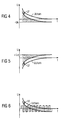
- the effective discharge voltage is due to the voltage range between -Ue and - Given Ue + Uf. This range is shown in FIG. 4 (and also in FIG Figures 5 and 6) hatched.
- the erase voltage periodically reversed as in Figure 5 using a Discharge curve for over-erased pixels shown. hereby can also be called over-erased image pixels in a defined, discharged state.
- the speed The polarity reversal can vary depending on the material Have values.
- Umpolungsvorgang can also be a low-frequency AC voltage can be used, as in Figure 6 based on a Discharge curve with AC voltage shown. In this case you can delete all pixels of a display with the same signal, regardless of their original state of charge.
- the active erase pulse with a voltage greater than the activation voltage Uf causes a very fast, but inaccurate Clear. After that, all discharged pixels can go over one longer period of time with the periodically reversed DC voltage Ue (with a value just below the activation voltage Uf) - continue to be deleted. This can be, for example during subsequent refresh cycles.
Landscapes
- Engineering & Computer Science (AREA)
- Physics & Mathematics (AREA)
- Computer Hardware Design (AREA)
- General Physics & Mathematics (AREA)
- Theoretical Computer Science (AREA)
- Control Of Indicators Other Than Cathode Ray Tubes (AREA)
Priority Applications (2)
| Application Number | Priority Date | Filing Date | Title |
|---|---|---|---|
| EP04015547A EP1577875A1 (fr) | 2004-03-17 | 2004-07-01 | Commande de dispositif d'affichage electrochromique |
| PCT/EP2004/053353 WO2005098812A1 (fr) | 2004-03-17 | 2004-12-08 | Commande d'affichages electrochromes |
Applications Claiming Priority (3)
| Application Number | Priority Date | Filing Date | Title |
|---|---|---|---|
| EP04006434 | 2004-03-17 | ||
| EP04006434 | 2004-03-17 | ||
| EP04015547A EP1577875A1 (fr) | 2004-03-17 | 2004-07-01 | Commande de dispositif d'affichage electrochromique |
Publications (1)
| Publication Number | Publication Date |
|---|---|
| EP1577875A1 true EP1577875A1 (fr) | 2005-09-21 |
Family
ID=34839789
Family Applications (1)
| Application Number | Title | Priority Date | Filing Date |
|---|---|---|---|
| EP04015547A Withdrawn EP1577875A1 (fr) | 2004-03-17 | 2004-07-01 | Commande de dispositif d'affichage electrochromique |
Country Status (2)
| Country | Link |
|---|---|
| EP (1) | EP1577875A1 (fr) |
| WO (1) | WO2005098812A1 (fr) |
Cited By (1)
| Publication number | Priority date | Publication date | Assignee | Title |
|---|---|---|---|---|
| DE102006017579B3 (de) * | 2006-04-13 | 2007-05-24 | Infineon Technologies Ag | Ansteuerschaltung für ein Zündelement eines Sicherheitssystems |
Citations (1)
| Publication number | Priority date | Publication date | Assignee | Title |
|---|---|---|---|---|
| US4175836A (en) * | 1976-08-31 | 1979-11-27 | Xerox Corporation | Method and apparatus for forming visible images |
-
2004
- 2004-07-01 EP EP04015547A patent/EP1577875A1/fr not_active Withdrawn
- 2004-12-08 WO PCT/EP2004/053353 patent/WO2005098812A1/fr not_active Ceased
Patent Citations (1)
| Publication number | Priority date | Publication date | Assignee | Title |
|---|---|---|---|---|
| US4175836A (en) * | 1976-08-31 | 1979-11-27 | Xerox Corporation | Method and apparatus for forming visible images |
Cited By (1)
| Publication number | Priority date | Publication date | Assignee | Title |
|---|---|---|---|---|
| DE102006017579B3 (de) * | 2006-04-13 | 2007-05-24 | Infineon Technologies Ag | Ansteuerschaltung für ein Zündelement eines Sicherheitssystems |
Also Published As
| Publication number | Publication date |
|---|---|
| WO2005098812A1 (fr) | 2005-10-20 |
Similar Documents
| Publication | Publication Date | Title |
|---|---|---|
| WO2005098811A1 (fr) | Commande d'affichages electrochromes | |
| DE3432991C2 (fr) | ||
| DE3853893T2 (de) | Flüssigkristallvorrichtung. | |
| DE68920531T2 (de) | Ansteuerschaltung für ein Matrixanzeigegerät. | |
| DE2508619C2 (de) | Verfahren zum Treiben einer Flüssigkristall-Anzeigematrix | |
| DE69629985T2 (de) | Verfahren und Einrichtung zur Steuerung einer Flüssigkristallanzeige mit Vorladen von Anzeigedatenleitungen | |
| DE3785687T2 (de) | Steuergeraet. | |
| DE69434493T2 (de) | Spannungserzeugungsschaltung, Steuerungsschaltung für gemeinsame Elektrode, Steuerungsschaltung für Signalleitung und Grauskala-Spannungserzeugungsschaltung für Anzeigevorrichtungen | |
| DE68929223T2 (de) | Flüssigkristallanzeigevorrichtung | |
| DE3711823C2 (fr) | ||
| DE60303965T2 (de) | Elektrophoretische anzeigevorrichtung | |
| DE3886838T2 (de) | Wiedergabeanordnung und Verfahren zum Steuern einer derartigen Wiedergabeanordnung. | |
| DE2449543B2 (de) | Verfahren zum Treiben einer Flüssigkristall-Matrixanzeigeeinheit | |
| DE10025252A1 (de) | Verfahren und System zum Ansteuern von Datenleitungen und eine das Verfahren und System verwendende Flüssigkristallanzeigevorrichtung | |
| DE69320438T2 (de) | Flüssigkristallanzeigeeinheit und elektronisches gerät unter verwendung dieser einheit | |
| DE3902834A1 (de) | Schaltungsanordnung zum betreiben einer bildwiedergabematrix | |
| DE3346271A1 (de) | Verfahren zum treiben einer aktiven matrix-anzeigevorrichtung | |
| DE102008005855A1 (de) | Flüssigkristallanzeigevorrichtung und Verfahren zum Treiben derselben | |
| DE3526321A1 (de) | Fluessigkristall-anzeigevorrichtung | |
| DE69123605T2 (de) | System zum schreiben von daten auf einer elektrophoretischen anzeigetafel. | |
| DE69828158T2 (de) | Vorrichtung zur steuerung einer matrixanzeigestelle | |
| DE3902832A1 (de) | Schaltungsanordnung zum betreiben einer bildwiedergabematrix | |
| DE2523763A1 (de) | Verfahren zum betrieb einer fluessigkristall-anzeige | |
| DE2608119A1 (de) | Schaltkreis zum abtasten und auffrischen eines halbleiterspeichers | |
| DE102005053003A1 (de) | Verfahren und Vorrichtung zum Ansteuern einer Flüssigkristall-Anzeigevorrichtung |
Legal Events
| Date | Code | Title | Description |
|---|---|---|---|
| PUAI | Public reference made under article 153(3) epc to a published international application that has entered the european phase |
Free format text: ORIGINAL CODE: 0009012 |
|
| AK | Designated contracting states |
Kind code of ref document: A1 Designated state(s): AT BE BG CH CY CZ DE DK EE ES FI FR GB GR HU IE IT LI LU MC NL PL PT RO SE SI SK TR |
|
| AX | Request for extension of the european patent |
Extension state: AL HR LT LV MK |
|
| 17P | Request for examination filed |
Effective date: 20060306 |
|
| AKX | Designation fees paid |
Designated state(s): DE FR GB IT |
|
| RAP1 | Party data changed (applicant data changed or rights of an application transferred) |
Owner name: SIEMENS AKTIENGESELLSCHAFT |
|
| RAP1 | Party data changed (applicant data changed or rights of an application transferred) |
Owner name: SIEMENS AKTIENGESELLSCHAFT |
|
| STAA | Information on the status of an ep patent application or granted ep patent |
Free format text: STATUS: THE APPLICATION IS DEEMED TO BE WITHDRAWN |
|
| 18D | Application deemed to be withdrawn |
Effective date: 20140201 |