EP1580844A1 - Phasenschieber mit linearer Polarisation und einer durch mems-Schalter variablen Resonanzlänge - Google Patents
Phasenschieber mit linearer Polarisation und einer durch mems-Schalter variablen Resonanzlänge Download PDFInfo
- Publication number
- EP1580844A1 EP1580844A1 EP05290642A EP05290642A EP1580844A1 EP 1580844 A1 EP1580844 A1 EP 1580844A1 EP 05290642 A EP05290642 A EP 05290642A EP 05290642 A EP05290642 A EP 05290642A EP 1580844 A1 EP1580844 A1 EP 1580844A1
- Authority
- EP
- European Patent Office
- Prior art keywords
- slot
- cell according
- ground plane
- resonant
- mems
- Prior art date
- Legal status (The legal status is an assumption and is not a legal conclusion. Google has not performed a legal analysis and makes no representation as to the accuracy of the status listed.)
- Granted
Links
- 230000010287 polarization Effects 0.000 title claims abstract description 16
- 230000010363 phase shift Effects 0.000 claims abstract description 30
- 230000008878 coupling Effects 0.000 claims description 12
- 238000010168 coupling process Methods 0.000 claims description 12
- 238000005859 coupling reaction Methods 0.000 claims description 12
- 239000006185 dispersion Substances 0.000 claims description 7
- 239000008188 pellet Substances 0.000 claims description 7
- 244000027321 Lychnis chalcedonica Species 0.000 claims description 4
- 230000002093 peripheral effect Effects 0.000 claims description 3
- 239000000758 substrate Substances 0.000 description 29
- XAGFODPZIPBFFR-UHFFFAOYSA-N aluminium Chemical compound [Al] XAGFODPZIPBFFR-UHFFFAOYSA-N 0.000 description 4
- 229910052782 aluminium Inorganic materials 0.000 description 4
- PNEYBMLMFCGWSK-UHFFFAOYSA-N aluminium oxide Inorganic materials [O-2].[O-2].[O-2].[Al+3].[Al+3] PNEYBMLMFCGWSK-UHFFFAOYSA-N 0.000 description 4
- 239000004020 conductor Substances 0.000 description 4
- PCHJSUWPFVWCPO-UHFFFAOYSA-N gold Chemical compound [Au] PCHJSUWPFVWCPO-UHFFFAOYSA-N 0.000 description 4
- 229910052737 gold Inorganic materials 0.000 description 4
- 239000010931 gold Substances 0.000 description 4
- 238000000034 method Methods 0.000 description 4
- 230000009977 dual effect Effects 0.000 description 3
- 238000001465 metallisation Methods 0.000 description 3
- 230000006978 adaptation Effects 0.000 description 2
- 230000003247 decreasing effect Effects 0.000 description 2
- 238000000151 deposition Methods 0.000 description 2
- 230000000694 effects Effects 0.000 description 2
- 238000005530 etching Methods 0.000 description 2
- 230000001939 inductive effect Effects 0.000 description 2
- 230000003071 parasitic effect Effects 0.000 description 2
- 238000011002 quantification Methods 0.000 description 2
- 230000015572 biosynthetic process Effects 0.000 description 1
- 230000000295 complement effect Effects 0.000 description 1
- 150000001875 compounds Chemical class 0.000 description 1
- 238000010586 diagram Methods 0.000 description 1
- 238000005516 engineering process Methods 0.000 description 1
- 239000011521 glass Substances 0.000 description 1
- 238000005286 illumination Methods 0.000 description 1
- 239000007937 lozenge Substances 0.000 description 1
- 238000013021 overheating Methods 0.000 description 1
- 244000045947 parasite Species 0.000 description 1
- 230000000737 periodic effect Effects 0.000 description 1
- 230000000704 physical effect Effects 0.000 description 1
- 230000001902 propagating effect Effects 0.000 description 1
- 230000005855 radiation Effects 0.000 description 1
- 229910052710 silicon Inorganic materials 0.000 description 1
- 239000010703 silicon Substances 0.000 description 1
- 239000004575 stone Substances 0.000 description 1
- 239000013589 supplement Substances 0.000 description 1
- 239000011800 void material Substances 0.000 description 1
Images



Classifications
-
- H—ELECTRICITY
- H01—ELECTRIC ELEMENTS
- H01Q—ANTENNAS, i.e. RADIO AERIALS
- H01Q15/00—Devices for reflection, refraction, diffraction or polarisation of waves radiated from an antenna, e.g. quasi-optical devices
- H01Q15/23—Combinations of reflecting surfaces with refracting or diffracting devices
-
- H—ELECTRICITY
- H01—ELECTRIC ELEMENTS
- H01P—WAVEGUIDES; RESONATORS, LINES, OR OTHER DEVICES OF THE WAVEGUIDE TYPE
- H01P1/00—Auxiliary devices
- H01P1/18—Phase-shifters
-
- H—ELECTRICITY
- H01—ELECTRIC ELEMENTS
- H01Q—ANTENNAS, i.e. RADIO AERIALS
- H01Q21/00—Antenna arrays or systems
- H01Q21/0006—Particular feeding systems
- H01Q21/0018—Space- fed arrays
Definitions
- the invention relates to the field of reflector array antennas (or "Reflectarray antennas"), and more particularly the phase-shifter cells who equip such antennas.
- Antenna reflector network is one of the two main families of antennas network, the other family consisting of antennas phased array (or "Phased Array Antennas"). These network antennas are particularly interesting because they can be reconfigured, for example to allow the passage of a zone of cover (or “spot”) to another.
- a reflector array antenna consists of radiating elements intercepted with minimal losses of waves, including signals to be transmitted, delivered by a primary source, in order to reflect them in a chosen direction, called the pointing direction.
- each radiating element is equipped with a phase control device with which it constitutes a cell passive or active phase shifter.
- phase-shifting cell is meant here as well the structures to cavity and radiating slit as planar resonant structures to paved radiating (or “patch”).
- the invention more particularly targets phase-shifting cells active, linearly polarized.
- a cell phase shifter provided with either a switch (or switch) consisting of diodes (usually PIN type), or MESFETs, or varactors, either mechanical control means (for example an engine charged with moving a dielectric bar).
- Switched phase shifters consume an important amount of energy and are subject to significant losses and overheating.
- Mechanically controlled phase shifters are complex to put particularly in the case of large networks, and energy consumers. In either case, the disadvantages induced by the phase control techniques used limit the applications of phase-shifting cells, particularly in the space domain and more specifically in observation platforms such as satellites.
- the purpose of the invention is therefore to improve the situation in the case of reflective grating antennas with active polarization phase shifters linear.
- phase-shifting cell presenting a resonant length characteristic and comprising in at least one place chosen a micron electromechanical device, of the MEMS type (for "Micro ElectroMechanical System"), which can be placed in at least two different states allowing and prohibiting the establishment of a short circuit intended to vary the resonant characteristic length, so to vary the phase shift of the waves to reflect which present at least a linear polarization.
- MEMS Micro ElectroMechanical System
- Each MEMS device may for example comprise a flexible bridge conductor whose states are controlled by two electrodes of control substantially superimposed and one of which is constituted by the bridge.
- each MEMS device may comprise a flexible beam suspended conductor (or "cantilever") whose states are controlled by a control electrode placed below its suspended part.
- the cell may comprise a planar resonant structure comprising at least one upper block rectangular placed substantially parallel to a lower ground plane, at a selected distance, the lower ground plane defining at least one Conductive "pad", for example rectangular, fully surrounded a non-conductive zone, placed below the upper pavement and dimensions smaller than his.
- the cell less a metallized crossing connecting the upper block to the pellet, and the MEMS device is placed at the level of the non-conductive area in order to establish in one of its states a connection between the pellet and the rest of the ground plane to control the resonant length of the upper pad.
- the lower ground plane can possibly define at least two pellets (for example rectangular) completely surrounded by a zone non-conductive, placed below the upper pad and dimensions less than his.
- the cell comprises at least two metallized crossings respectively connecting the upper pavement to one of the pellets, and at least two MEMS devices each placed at the level of one of the non-conducting areas in order to establish links between the one less lozenges and the rest of the ground plane, thus allowing to define at least three resonant lengths of different upper pavement according to their states.
- the cell can have a top ground plane including at least one slot radiating, provided with a MEMS device controlling its resonant length characteristic, a lower ground plane, and metallic crossings connecting the lower ground plane to the peripheral parts of the plane of higher mass in order to define a resonant cavity.
- the plan of upper mass may comprise at least two radiating slots each provided with a single MEMS device controlling their length resonant characteristic. Each MEMS device can then be preferentially placed substantially in the middle of a radiating slot.
- the slots are preferably substantially parallel to each other and may have slightly different lengths. But, they can also have a curved shape, so as to achieve together a short annular slot circuited at two substantially opposite points.
- the upper ground plane may comprise a slot radiator, provided with at least two MEMS devices for defining at least three different resonant lengths depending on their states.
- the higher ground plane can possibly comprise at least one rectangular radiating slot having long sides parallel to a first direction, and at least one other slot radiating rectangular with long sides parallel to a second direction perpendicular to the first, to allow a double linear polarization.
- the cell may comprise a planar resonant structure comprising a top paver placed substantially parallel to a lower ground plane at a distance chosen.
- the block comprises at least one slot provided with at least a MEMS device controlling its characteristic resonant length.
- the cell can then comprise a single slot (of length half wave) provided with at least two MEMS devices, allowing to define at least three different resonant lengths depending on their states.
- the upper block may be substantially square, and the cell may comprise at least first and second rectangular slots (in length quarter wave) placed substantially opposite one another, leading to two opposite non-radiating sides of the square, and each having minus two MEMS devices to define at least three lengths resonant different according to their states.
- the cell can also include at least third and fourth slots rectangular (of quarter-wave length) placed substantially opposite from each other, leading to two other opposite non-radiating sides square, and each having at least two MEMS devices, to define at least three other different resonant lengths according to their states, to allow a linear double polarization.
- We can also provide several upper pavers each provided with at least half a slot quarter of wave, pairs of half-slots facing each other then constituting half wave slots.
- the bridge In the presence of a bridge MEMS device and slot (s) rectangular (s), the bridge is preferably placed substantially parallel to the long sides of the slot.
- the bridge In the presence of a MEMS device with beam and slot (s) rectangular (s), said beam is preferentially placed substantially perpendicular to large sides of the slot.
- the lower ground plane can define a lower pavement placed below the upper block and of dimensions smaller than his
- the cell comprises metallized vias which connect the plane mass to peripheral parts of the upper pavement in order to define a resonant cavity.
- This paved and cavity structure defines yet another family of dephasing cells.
- the invention also proposes a reflective array antenna equipped with at least two dephasing cells of the type presented above.
- the invention is particularly well adapted, although in a non exclusive, to Ku-band geostationary telecommunication antennas (12 to 18 GHz), with reconfigurable coverage (change of orbital position, adaptation of traffic), and to C-band radar antennas (4 to 8 GHz) or X band (8 to 12 GHz), in particular for SAR-type radars (radar synthetic opening).
- the invention relates to a polarization-active phase shifter cell linear for an active reflector array antenna.
- the reflector array antenna can for example be dedicated to telecommunications, for example of the Ku-band geostationary type (12 to 18 GHz), with reconfigurable coverage (change of orbital position or adaptation of traffic), or to C-band (4 to 8 GHz) or band radars X (8 to 12 GHz), especially for SAR type radars synthetic), or high-speed ISL-RF type links, in particular inside a small constellation of satellites flying in formation.
- telecommunications for example of the Ku-band geostationary type (12 to 18 GHz), with reconfigurable coverage (change of orbital position or adaptation of traffic), or to C-band (4 to 8 GHz) or band radars X (8 to 12 GHz), especially for SAR type radars synthetic), or high-speed ISL-RF type links, in particular inside a small constellation of satellites flying in formation.
- a phase-shifting cell comprises in one or more selected locations a device electromechanical micrometer, MEMS type (for "Micro ElectroMechanical System ").
- MEMS type for "Micro ElectroMechanical System ".
- Each MEMS device can be placed at using electrical controls, in at least two different states permitting and prohibiting respectively the establishment of a short circuit intended to vary a characteristic resonant length of the cell, in order to to vary the phase shift of the waves to be reflected (from the source of the antenna) having at least one linear polarization.
- phase-shifting cell can be divided into three major families according to its radiant structure.
- a first family groups together cavity and slit (s) radiating structures, a second family groups together resonant planar paved structures (or "patches") and a third family groups planar resonant cavity structures.
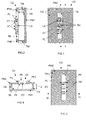
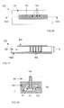
- FIGS. 1 and 2 is illustrated a first example of a cell CD phase shifter comprising a substrate SB having a "rear" face (or “lower”), secured to an "inferior” ground plane PM1, and a face “before” (or “superior”), solidarized to a plane of mass "Superior” PM2.
- the SB substrate is for example made of Duroid or TMM and has a thickness d equal, for example, to ⁇ / 4, where ⁇ is the length wave in the void of the waves to be reflected, coming from the source of the antenna.
- the ground planes lower PM1 and higher PM2 are connected electrically between them via holes (or bushings) TM metallized formed in SB substrate.
- These plans are for example made from alumina, silicon or glass substrates which, because of their their small thicknesses (typically 500 ⁇ m) must be reported on a SB substrate in Duroid or TMM so as to allow obtaining a thickness equal to ⁇ / 4.
- the metallized holes TM are preferentially implanted at the periphery of the lower mass planes PM1 and higher PM2 in order to define a resonant cavity.
- a first technique consists in superimposing a substrate in Duroid (or Metclad), for example with a thickness of about 3 mm, on a alumina substrate, for example with a thickness of approximately 0.254 mm, and then depositing a lower ground plane PM1 on the underside of the substrate in Duroid and an upper ground plane PM2, on the upper face of the alumina substrate, said upper ground plane PM2 being locally interrupted by the slits.
- Duroid or Metclad
- a second technique is to use only one substrate Duroid (or Metclad), for example of thickness equal to about 2 or 3 mm, then to form on its upper face portions of a plane of intermediate mass in which control lines are formed of tension, then to report on this upper face portions of alumina substrates, for example with a thickness of approximately 0.254 mm, having on an upper face an upper ground plane PM2 each having one or more slots and then depositing a ground plane lower PM1 on the underside of the Duroid substrate, and finally to connect the lower, middle and upper ground planes by two levels of holes (or traverses) metallized.
- Duroid or Metclad
- the upper ground plane PM2 comprises a single radiating slot FR, preferably of rectangular shape defined by two long sides (longitudinal), of length b, and two short sides (transverse), of width a.
- This radiating slot FR is for example made by etching the upper plane of mass PM2.
- the radiating slot FR has a resonance of parallel LC type.
- the parameters of such a resonator depend mainly on the length b and width a of the radiating gap FR, as well as the permittivity ⁇ r of the substrate SB.
- the cavity has a cutoff frequency equal to 18.75 GHz and operates only in its fundamental mode, this which corresponds to a guided wavelength ⁇ g equal to approximately 16.14 mm, in the case of an air cavity.
- phase shifts of up to 360 ° can be obtained for slot widths FR of between approximately 0.25 mm. and about 1 mm.
- the point of inflection of the phase shift is obtained at the resonance of the slot FR, which corresponds to a length b equal to about 5.5 mm, taking into account other values mentioned above.
- the radiating slot FR is preferentially centered in the middle of the upper mass plane PM2. But he could be otherwise, especially in the presence of a possible slot complementary parasite. In the latter case, the slots are located preferentially symmetrically with respect to the center of the cell.
- the radiating slot FR is provided with three MEMS DC devices each constituting a switch two-state.
- the radiating slot could have a number different from MEMS DC devices as long as it is at least equal to one.
- Each MEMS DC device here consists of a flexible bridge PT conductor whose two ends are secured to studs of holding PL themselves secured to the upper face of the substrate SB.
- These plots PL are for example made of gold or aluminum and have a thickness slightly greater than that of the upper ground plane PM2.
- the PT flexible bridge is made in the form of a blade made conductive, by example by metallization in gold or aluminum, and installed in the slot FR substantially parallel to its longitudinal edges.
- each MEMS DC device comprises two electrodes substantially superimposed control, one of them being constituted by the flexible bridge PT, and the other being, for example, placed at a level above the flexible bridge PT (not shown), these two electrodes being connected to a supply circuit (not shown).
- the suspended part of the PT bridge In the presence of a control current selected at the level of control electrodes, the suspended part of the PT bridge is drawn towards said LA access lines. The suspended part then flexes until it comes to contact of the two access lines LA, which locally generates a short circuit in the radiating slot FR and reduces its characteristic resonant length (b), which is its electrical length. This is one of the two states of the DC MEMS device.
- the PT bridge In the absence of control current, the PT bridge is remote from access lines LA, so that the length of the radiating gap FR is not disrupted. This is the other state of the MEMS DC device.
- Figures 3 and 4 is illustrated a second example of CD phase shifter cell of the first family. This is a variant of the phase-shifting cell CD described above with reference to FIGS. 1 and 2. More precisely, what differentiates the first embodiment of the second this is the embodiment of the MEMS devices.
- each MEMS device DC comprises a flexible beam (or “Cantilever") conductive PE having an end secured to a stud PL conductor, formed in the radiating slot FR along one longitudinal edges and electrically connected to the ground plane higher PM2.
- a flexible beam or "Cantilever" conductive PE having an end secured to a stud PL conductor, formed in the radiating slot FR along one longitudinal edges and electrically connected to the ground plane higher PM2.
- This pad PL ' is for example made of gold or aluminum and has a thickness slightly greater than that of the ground plane upper PM2, so that the beam PE is suspended above the radiating slot FR and the level of the upper ground plane PM2.
- Beam flexible PE is made in the form of a blade made conductive, by example using a metallization in gold or aluminum, installed substantially perpendicular to its longitudinal edges. The free end PE beam crosses the slot FR in its width and overflows slightly on the upper mass plane PM2 in a place where is preferentially placed an electrically conductive PLC contact pad.
- each MEMS device DC ' comprises a EC 'command placed below the suspended central part of the PE beam, and connected to a supply circuit (not shown), another electrode being constituted by the flexible conducting beam PE.
- the electrode of EC 'command is formed on the upper face of the SB substrate, inside of the radiating gap FR.
- the suspended part of the beam PE is attracted towards said electrode. She then flexes until her free end come into contact with the PLC contact pad, which locally generates a short circuit in the radiating slot FR and reduces its resonant length characteristic (b), which is its electrical length. This is one of the two states of the MEMS device DC '.
- the radiating slot FR is provided of three DC MEMS devices. But, the radiating slot FR could have a different number of MEMS devices DC 'when this one is at least equal to one.
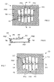
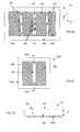
- FIGS. 5 and 6 is illustrated a third example of a cell CD phase shifter of the first family.
- N 5
- the number N of radiating slits illustrated is not limiting. It can take any higher value or equal to two.
- at least one of the slots is not equipped with a MEMS device.
- the radiating slots have, for some, lengths different. More precisely, in the illustrated example, the ground plane upper PM2 has two radiating end slots FR1, having a first characteristic resonant length L1, two slots intermediate radiators FR2, having a second length resonant characteristic L2 greater than L1, and a radiating slit central FR3, having a third characteristic resonant length L3 greater than L2. In one variant, the five slots could have five different lengths.
- the five radiating slots FR1 to FR3 are substantially centered with respect to the middle of the upper mass plane PM2, and their MEMS DC PT bridge device is also installed in centered position. But, we could do differently. Indeed, in the example described above we run around the undesirable slots, but we could also modify the resonant length of some of them to excite several resonances and well control the phase shift between slots, with the coupling.
- the distance separating two adjacent slits may be fixed or variable. It varies according to the needs. It is typically between about 100 ⁇ m and 500 ⁇ m.
- Each slot short-circuited in the middle acts as it were as a parasitic element for the neighboring non-shorted slot. It's about here to excite several resonances to have a range of phase shifts acceptable, while avoiding a very resonant response leading to low band performance.
- the coupling between the different resonances achieved by coupling between a slot and a pad (or patch), can mitigate the resonant answer.
- FIGS. 7 and 8 is illustrated a fourth example of CD phase shifter cell of the first family. This is a variant of the CD phase-shifting cell described above with reference to Figures 5 and 6.
- each MEMS DC device with a PT bridge is indeed replaced by a MEMS DC 'PE beam device, of the type of those described in reference to Figures 3 and 4.
- phase-shifting cell CD The operation of this phase-shifting cell CD is identical to that of the phase-shifting cell described above with reference to FIGS. 5 and 6.
- At least one radially oriented FRV slot is used in a first direction ("vertical"), and at least one radiating slot HRF oriented in a second ("horizontal") direction, perpendicular to the first one.
- the cell CD phase shifter may have one or more FRV radiating slots and one or more FRH radiating slots as required.
- the cell is then preferably rectangular and has a width substantially equal to half of its length.
- FRV and FRH radiating slots having only one MEMS device with PT bridge or PE beam, but however, it is preferable to use FRV and FRH radiating slots having at least two PT bridge or PE beam MEMS devices (as shown).
- FIGS 10 and 11 is illustrated a first example of CD phase-shifting cell comprising a substrate SB having a face back (or lower), secured to a lower ground plane PM1 defining a lower tile (or “patch”), and a front (or upper) face, solidarized to a higher ground plane defining a block (or "patch") higher PS.
- the upper PS and lower PM1 tiles define a planar resonant structure.
- the SB substrate is for example made of Duroid or TMM and has a thickness of weak, typically of the order of ⁇ / 10 to ⁇ / 5, where ⁇ is the wavelength in the vacuum of the waves to reflect, coming from the source of the antenna.
- the upper block PS is placed substantially parallel to the plane lower mass PM1 and has dimensions smaller than hers.
- the upper PS pad is shaped rectangular, and preferentially square.
- the upper block PS has a single slot FP, preferentially of rectangular shape defined by two long sides (longitudinal), of length b, and two small sides (transverse), of width at.
- This slot FP is for example made by etching the plane of mass constituting the upper pavement PS.
- the slot FP is provided with three MEMS DC devices with PT bridge each constituting a two-way switch states, of the type of those described above with reference to Figures 1 and 2.
- the FP slot could have a different number of MEMS DC devices as long as it is at least one.
- the operating principle of this phase-shifting cell CD is identical to that described previously with reference to Figures 1 and 2. Only the physical effect involved differs.
- the slot FP is here intended to disrupt the path of currents that circulate in the upper pavement PS.
- FIG. 12 is illustrated a second example of a cell CD dephaser of the second family. This is a variant of the cell CD phase shifter described above with reference to Figures 10 and 11. More precisely, what differentiates the first embodiment of the second this is the embodiment of the MEMS devices.
- each MEMS device DC ' is of PE beam type, as in the embodiment described above with reference to Figures 3 and 4.
- the disturbing slot FP is equipped with three MEMS DC devices. But, the disruptive crack FP could have a different number of MEMS devices DC 'when this one is at least equal to one.
- the third example illustrated in FIG. 13 has two holes (or crossings) metallized TM to couple electrically the upper pavement PS and the lower ground plane PM1 of either side of the two opposite ends of the disturbing slot FP.
- These MT metallized holes are intended to supply DC power to the pavement higher PS so as to bias the MEMS device.
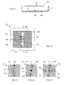
- the upper pavement PS has two small disturbing slots F1 and F2, whose resonance is approximately one quarter of the length wave, placed substantially opposite one another and opening onto opposite, non-radiating edges.
- Each small slot F1, F2 is provided of at least one (here two) MEMS device with PT bridge (but it could be a PE beam).
- a hole (or crossing) metallized TM allows electrically couple the upper PS block and the lower ground plane PM1 in a central part located between the two small slots disruptive F1 and F2.
- This metallized hole MT is intended to supply direct current the upper pad PS so as to bias the device MEMS.
- the PS upper pad (substantially square) includes only a rectangular slot opening on a non-radiating side of the square and having at least two devices MEMS DC or DC '.
- small split a disturbing FP slot of the type shown above in reference to Figure 14.
- small disturbing slots F1 to F4 quarter-wave length, with only a single MEMS bridge device PT or PE beam, but it is however preferable to use small disruptive slots F1 to F4 having at least two MEMS devices to PT bridge or PE beam (as shown).
- the number of MEMS devices used in each slot depends on the number of phase states that one wish to obtain.
- a hole (or crossing) metallized TM makes it possible to electrically couple the upper block PS and the plane of lower mass PM1 in a central part located between the four small disruptive slots F1 to F4 of quarter-wave length.
- This MT metallized hole is intended to supply DC power to the upper pad PS so as to polarize the MEMS device.
- the upper PS block is powered by at least one hole Metallic TM.
- this feed can be carried out by means of a quarter-wave line with high impedance.
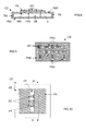
- FIG. 16 to 18 is illustrated a sixth example of CD phase-shifting cell comprising a substrate SB having a face back (or lower), secured to a lower ground plane PM1, and a front (or upper) side, secured to a ground plane upper defining a patch (or patch) upper PS 'shape rectangular.
- the upper pavement PS 'and the lower ground plane PM1 constitute a short-circuited cobblestone structure that defines a structure planar resonant. It is important to note that the length of the pavement higher PS is chosen so that it is resonant at ⁇ / 4.
- the SB substrate is for example made of Duroid or TMM and has a thickness of weak, typically of the order of ⁇ / 10 to ⁇ / 5, where ⁇ is the wavelength in the vacuum of the waves to reflect, coming from the source of the antenna.
- the upper pavement PS ' is placed substantially parallel to the plane lower mass PM1 and has much smaller dimensions than at least in one direction.
- the lower ground plane PM1 has at least one small conductive "pellet" PI, isolated from its own conductive part by a non-conducting zone Z, made for example by engraving.
- Each small conductive pad Pl is electrically connected to the upper pavement PS 'via a hole (or crossing) metallized TM.
- each small conductive pad P1 is preferably rectangular shape, and more preferably square.
- Each metallized hole TM is connected to the upper pavement PS 'in one chosen place, the different places being preferentially aligned along a straight line parallel to the longitudinal sides of said pavement higher PS.
- each small conductive pad PI is provided with a MEMS device with PT bridge or with PE beam (as illustrated in FIG. 18), of the type described above.
- Each MEMS device DC '(or DC) is intended to establish an electrical connection between its lower pavement Pl and the conductive part of the lower ground plane PM1, when placed in his first state (bent). So when one of the devices MEMS DC '(or DC) is placed in its first state (flexed), the metallized hole TM, which is connected at its small conductive pad Pl, bypasses the upper pad PS ' substantially at the point where it is connected to it, which has the effect of vary its characteristic resonant length (or electrical length) and therefore the phase shift of the reflected wave.
- This structure is advantageous because its devices are placed on the backside they are further protected from radiation.
- five metallized holes TM make it possible to define five short circuits corresponding to at least six different resonant lengths for the upper pad PS '. Therefore, by separately controlling the different MEMS devices DC '(or DC), it is possible to obtain several different phase shifts of the wave reflected by the CD phase shifter cell.
- phase-shifting cell CD may comprise a number MEMS devices (DC or DC ') different from five, provided that the latter is less equal to one.
- the number of MEMS devices used depends on the number of phase states that one wishes to obtain.
- the sum of the length of the "active" dipole (that is to say between the short circuit and the other end of the dipole) and the length of the short-circuit must be equal to one quarter of the wavelength of the guided mode ⁇ g .
- This embodiment may allow the constitution of a cell linear polarization phase shifter, of the type illustrated in FIG. figure 9. To do this, it is necessary to combine "horizontal" dipoles with “vertical” dipoles of the type described above with reference to FIGS. 16 to 18.
- This exemplary embodiment constitutes, in a way, a structure intermediate between the exemplary embodiments illustrated in FIGS. 5 to 8 and the exemplary embodiments illustrated in FIGS. 10 to 12.
- the phase shifter cell CD comprises a substrate SB comprising a rear face (or lower), secured to a lower ground plane PM1, and a front face (or upper), secured to an upper pad PS.
- the SB substrate is for example made of Duroid or TMM and has a thickness d equal to ⁇ / 4, where ⁇ is the wavelength in the vacuum waves to reflect, from the source of the antenna.
- the substrate SB is crossed, on its periphery, by holes (or crossings) TM connected to the lower ground plane PM1 and surrounding the upper pad PS to define a resonant cavity.
- the upper pad PS is a square of length between about 15 mm and about 17 mm.
- the upper block PS has at least two (here five) radiating slots each having a single MEMS device (DC or DC ') with PT bridge or PE beam.
- the number N of slots radiating illustrated is not limiting. It can take any value greater than or equal to two.
- the slots have a large side of length between about 5 mm and about 7 mm, and a small side of width between about 0.3 mm and about 0.7 mm.
- the radiating slots have, for some, lengths different.
- the upper PS block has two radiating end slots FR1, presenting a first resonant length characteristic L1, two radiating slots intermediate FR2, having a second resonant length characteristic L2 greater than L1, and a central radiating slot FR3, having a third characteristic resonant length L3 greater than L2.
- the five slots could have five lengths different.
- the five radiating slots FR1 to FR3 are substantially centered relative to the middle of the upper PS block, and their devices MEMS DC to PT bridge (or DC 'to PE beam) are also installed in centered position (for example).
- Each slot short-circuited in the middle acts as it were as a parasitic element for the neighboring non-shorted slot. By therefore, it is likely to improve the bandwidth of the slot not short-circuited.
- the slots which are not desirable, but we could proceed differently.
- Some holes (or crossings) metallized TM can be advantageously used to route orders voltage at the different MEMS devices DC or DC '.
- each slot of half-wave length is consisting of two half-slits of quarter-wave length.
- the devices MEMS DC or DC ' have been voluntarily omitted so as not to overburden the drawings.
- two upper pavers PS1 and PS2 are placed substantially parallel to the lower ground plane PM1 and away from it. These two upper pavers PS1 and PS2 are spaced from each other by a selected distance so as to define between them a capacitive area. They have different shapes and each a half quarter wave slot FR1, FR2. These two half slits FR1 and FR2 together constitute a half-wave slot and an inductive zone whose effect is advantageously compensated (at least partially) by the inter-paved capacitive area.
- the pavers have a width equal to about 3.7 mm and are separated by a distance, forming a slot, equal to about 0.1 mm.
- Such an asymmetrical structure offers a frequency response of good stability due to an effective coupling between the two resonances.
- both upper pavers PS1 and PS3 are substantially identical and frame the PS2 pad.
- both upper pavers PS1 and PS3 each have half a quarter slit wave FR1, FR4, while the upper pad PS2 has two halves quarter-wave slots FR2 and FR3 opening on two opposite sides, one placed next to the half slot FR1 of the upper block PS1 and defining with it a first half wave slit, and the other placed next to the half slot FR4 of the upper block PS3 and defining with it a second split half wave.
- Such a symmetrical structure also offers an answer in frequency of good stability due to effective coupling between resonances.
- phase-shifting cells which comprise at least one block provided with at least one slot FP, described above, one or more auxiliary blocks and at least one MEMS device of coupling, so as to vary the size of the pavement according to at least one of its two directions (X and Y), and preferably along its length X which is parallel to the direction defining the length b (or long side) of the slots FP.
- a CD phase shifter cell of this type is illustrated in FIG.
- the phase-shifting cell CD illustrated in FIG. 23 from a structure of the type illustrated in Figures 10 to 12. It therefore comprises a substrate SB having a rear face (or lower), secured to a lower mass plane PM1, and a front face (or upper), secured to at least one block (or patch) upper PS and to minus one auxiliary pad PA1, PA2.
- auxiliary blocks PA1 and PA2 placed on both sides of two parallel sides of the PS pad (themselves parallel to the long sides (Y) of the FP slot).
- the upper pavers PS, PA1 and PA2 and the lower ground plane PM1 define a resonant planar structure.
- the phase-shifting cell CD also comprises at least one device DC or DC Coupling MEMS 'Installed Between PS Keypad and Auxiliary Keypad PA1, PA2 and responsible for establishing, or not, a contact between these blocks according to the state in which he is placed.
- the PS block is likely to be connected to each auxiliary pad PA1, PA2 via three MEMS devices DC ', a central and two end.
- the two devices MEMS DC ' end are preferably placed symmetrically with respect to the center of the auxiliary pad PA1, PA2.
- the different DC or DC MEMS devices that connect the PS pad to one of the auxiliary blocks PA1, PA2 are preferably controlled by the same control current. In other words, they are preferentially placed simultaneously in the same state so as to ensure either an electrical connection or an absence of an electrical connection, between the PS block and the auxiliary block PA1, PA2 concerned.
- the physical length (according to X) of the PS pad can therefore be increased.
- the possibility of controlling the dispersion of this phase shift in frequency is particularly interesting for to compensate for the frequency-dispersive illumination of a plane reflector by a primary source.
- pavers auxiliaries may be placed parallel to each other, on at least one of the two sides of the pavement PS, the tiles being connected in pairs by one or more MEMS devices coupling DC 'or DC, and preferably three. This makes it possible to vary even more the physical length of the PS block, as needed, in playing on the respective states of the MEMS devices DC 'or DC coupling the auxiliary pavers.
- auxiliary pavers which are located on both sides of two parallel sides of the PS block do not necessarily have the same dimensions. This is particularly the case in the example illustrated on the Figure 23, where the auxiliary pad PA1 has a length (in the direction X) greater than that of the auxiliary pad PA2, but a width (according to the direction Y) substantially identical to that of the auxiliary pad PA2.
- the length of the PS pad is equal to L
- the lengths of the tiles auxiliary PA1 and PA2 can be respectively equal to L / 2 and L / 3.
- the PS block can have one or more MEMS devices DC or DC '. Number of MEMS devices used depends on the number of phase shift states that one wish to obtain.
- phase-shifting cell CD therefore makes it possible to vary dynamically, as needed, the phase shift and dispersion of frequency phase, which is particularly advantageous for a active antenna (or reconfigurable).
- the choice of phase shift and dispersion of the phase shift is indeed fixed by the physical length of the PS pad and by the electrical length of each FP slot of each PS pad, according to the states respective MEMS devices used.
- Such a structure CD therefore comprises a substrate SB comprising a rear face (or lower), secured to a lower ground plane PM1, and a front face (or upper), secured to at least one block (or patch) PS upper having at least one FP slot.
- the upper pad PS and the lower mass plane PM1 define a resonant planar structure.
- the dimensions of the upper PS block, and in particular its length x (in the X direction), and the slot FP, and in particular its length b (in the Y direction), as well as the thickness d of substrate SB it is possible to impose both a chosen phase shift and a dispersion selected frequency phase.
- the upper PS block When the upper PS block has only one FP slot, it is preferably placed substantially at its center. But, the pavement PS could have multiple FP slots, possibly different dimensions.
- phase-shifting cell CD makes it possible to obtain any phase shift, and in particular phase shifts (very) greater than 360 °. It also controls the dispersion of this phase shift in frequency.
- the phase-shifting cells of the prior art which make it possible to obtain such characteristics, comprise three blocks placed parallel to one another above and above a lower ground plane (they are described in particular in the article by JA Encinar et al, "Design of a three-layer printed reflectarray for dual polarization and dual coverage", 27 th ESA Antenna workshop, Santiago Compostel, Spain, March 2004).
- the phase-shifter cells CD according to the invention comprise only one level of metallization (upper block), in addition to the lower ground plane PM1, and are therefore much simpler to achieve than the phase-shifting cells of the prior art.
Landscapes
- Variable-Direction Aerials And Aerial Arrays (AREA)
- Waveguide Aerials (AREA)
- Piezo-Electric Or Mechanical Vibrators, Or Delay Or Filter Circuits (AREA)
- Waveguide Switches, Polarizers, And Phase Shifters (AREA)
Applications Claiming Priority (2)
| Application Number | Priority Date | Filing Date | Title |
|---|---|---|---|
| FR0450575A FR2868216B1 (fr) | 2004-03-23 | 2004-03-23 | Cellule dephaseuse a polarisation lineaire et a longueur resonante variable au moyen de commutateurs mems |
| FR0450575 | 2004-03-23 |
Publications (2)
| Publication Number | Publication Date |
|---|---|
| EP1580844A1 true EP1580844A1 (de) | 2005-09-28 |
| EP1580844B1 EP1580844B1 (de) | 2009-06-17 |
Family
ID=34855227
Family Applications (1)
| Application Number | Title | Priority Date | Filing Date |
|---|---|---|---|
| EP05290642A Expired - Lifetime EP1580844B1 (de) | 2004-03-23 | 2005-03-23 | Phasenschieber mit linearer Polarisation und einer durch mems-Schalter variablen Resonanzlänge |
Country Status (6)
| Country | Link |
|---|---|
| US (1) | US7358915B2 (de) |
| EP (1) | EP1580844B1 (de) |
| AT (1) | ATE434276T1 (de) |
| DE (1) | DE602005014900D1 (de) |
| ES (1) | ES2327650T3 (de) |
| FR (1) | FR2868216B1 (de) |
Cited By (3)
| Publication number | Priority date | Publication date | Assignee | Title |
|---|---|---|---|---|
| EP1881557A1 (de) * | 2006-07-07 | 2008-01-23 | Fondazione Torino Wireless | Antenne, Herstellungsverfahren für eine Antenne und Vorrichtung zur Herstellung einer Antenne |
| EP2273617A1 (de) * | 2009-06-09 | 2011-01-12 | Broadcom Corporation | Verfahren und System zum Konfigurieren einer Leckwellenantenne unter Nutzung von elektromechanischen Mikrosystemen |
| CN103345057A (zh) * | 2013-05-31 | 2013-10-09 | 华中科技大学 | 一种微型的桥式结构及其制备方法 |
Families Citing this family (26)
| Publication number | Priority date | Publication date | Assignee | Title |
|---|---|---|---|---|
| CN101438366B (zh) * | 2006-03-08 | 2011-10-26 | 维斯普瑞公司 | 微机电系统(mems)可变电容器、激励部件及相关方法 |
| CN103441339B (zh) * | 2006-04-27 | 2016-01-13 | 泰科电子服务有限责任公司 | 异向材料天线设备 |
| US7741933B2 (en) * | 2006-06-30 | 2010-06-22 | The Charles Stark Draper Laboratory, Inc. | Electromagnetic composite metamaterial |
| KR101086743B1 (ko) * | 2006-08-25 | 2011-11-25 | 레이스팬 코포레이션 | 메타물질 구조물에 기초된 안테나 |
| FR2907262B1 (fr) * | 2006-10-13 | 2009-10-16 | Thales Sa | Cellule dephaseuse a dephaseur analogique pour antenne de type"reflectarray". |
| US7855696B2 (en) * | 2007-03-16 | 2010-12-21 | Rayspan Corporation | Metamaterial antenna arrays with radiation pattern shaping and beam switching |
| US7724180B2 (en) * | 2007-05-04 | 2010-05-25 | Toyota Motor Corporation | Radar system with an active lens for adjustable field of view |
| GB0711382D0 (en) * | 2007-06-13 | 2007-07-25 | Univ Edinburgh | Improvements in and relating to reconfigurable antenna and switching |
| US8514146B2 (en) * | 2007-10-11 | 2013-08-20 | Tyco Electronics Services Gmbh | Single-layer metallization and via-less metamaterial structures |
| US7791552B1 (en) | 2007-10-12 | 2010-09-07 | The United States Of America As Represented By The Administrator Of The National Aeronautics And Space Administration | Cellular reflectarray antenna and method of making same |
| US20100109971A2 (en) * | 2007-11-13 | 2010-05-06 | Rayspan Corporation | Metamaterial structures with multilayer metallization and via |
| US8674792B2 (en) * | 2008-02-07 | 2014-03-18 | Toyota Motor Engineering & Manufacturing North America, Inc. | Tunable metamaterials |
| US20090206963A1 (en) * | 2008-02-15 | 2009-08-20 | Toyota Motor Engineering & Manufacturing North America, Inc. | Tunable metamaterials using microelectromechanical structures |
| US8547286B2 (en) * | 2008-08-22 | 2013-10-01 | Tyco Electronics Services Gmbh | Metamaterial antennas for wideband operations |
| US7965250B2 (en) * | 2008-10-02 | 2011-06-21 | Toyota Motor Engineering & Manufacturing North America, Inc. | Microwave lens |
| FR2936906B1 (fr) * | 2008-10-07 | 2011-11-25 | Thales Sa | Reseau reflecteur a arrangement optimise et antenne comportant un tel reseau reflecteur |
| US8212573B2 (en) | 2009-01-15 | 2012-07-03 | The Curators Of The University Of Missouri | High frequency analysis of a device under test |
| US8044874B2 (en) * | 2009-02-18 | 2011-10-25 | Harris Corporation | Planar antenna having multi-polarization capability and associated methods |
| US8681050B2 (en) | 2010-04-02 | 2014-03-25 | Tyco Electronics Services Gmbh | Hollow cell CRLH antenna devices |
| FR2980044B1 (fr) | 2011-09-14 | 2016-02-26 | Thales Sa | Cellule dephaseuse rayonnante reconfigurable basee sur des resonances fentes et microrubans complementaires |
| US9046605B2 (en) | 2012-11-05 | 2015-06-02 | The Curators Of The University Of Missouri | Three-dimensional holographical imaging |
| CN115149226B (zh) * | 2021-03-31 | 2023-08-25 | 北京京东方技术开发有限公司 | 移相器及其制备方法、天线 |
| WO2023106238A1 (ja) * | 2021-12-07 | 2023-06-15 | 京セラ株式会社 | 複合共振器および電波屈折板 |
| WO2023141759A1 (zh) * | 2022-01-25 | 2023-08-03 | 京东方科技集团股份有限公司 | 一种移相器及天线 |
| WO2023201466A1 (zh) * | 2022-04-18 | 2023-10-26 | 京东方科技集团股份有限公司 | 移相器及通信装置 |
| CN116259962B (zh) * | 2023-03-02 | 2024-08-20 | 中国人民解放军战略支援部队航天工程大学 | 一种采用谐振移相结构的反射型超表面单元及其阵列天线 |
Citations (3)
| Publication number | Priority date | Publication date | Assignee | Title |
|---|---|---|---|---|
| US6184839B1 (en) * | 1996-12-19 | 2001-02-06 | Lockheed Martin Missiles & Space Company | Large instantaneous bandwidth reflector array |
| US6388631B1 (en) * | 2001-03-19 | 2002-05-14 | Hrl Laboratories Llc | Reconfigurable interleaved phased array antenna |
| US20030122721A1 (en) * | 2001-12-27 | 2003-07-03 | Hrl Laboratories, Llc | RF MEMs-tuned slot antenna and a method of making same |
Family Cites Families (2)
| Publication number | Priority date | Publication date | Assignee | Title |
|---|---|---|---|---|
| US6417807B1 (en) * | 2001-04-27 | 2002-07-09 | Hrl Laboratories, Llc | Optically controlled RF MEMS switch array for reconfigurable broadband reflective antennas |
| US6307519B1 (en) * | 1999-12-23 | 2001-10-23 | Hughes Electronics Corporation | Multiband antenna system using RF micro-electro-mechanical switches, method for transmitting multiband signals, and signal produced therefrom |
-
2004
- 2004-03-23 FR FR0450575A patent/FR2868216B1/fr not_active Expired - Fee Related
-
2005
- 2005-03-23 US US11/086,304 patent/US7358915B2/en not_active Expired - Fee Related
- 2005-03-23 EP EP05290642A patent/EP1580844B1/de not_active Expired - Lifetime
- 2005-03-23 ES ES05290642T patent/ES2327650T3/es not_active Expired - Lifetime
- 2005-03-23 DE DE602005014900T patent/DE602005014900D1/de not_active Expired - Lifetime
- 2005-03-23 AT AT05290642T patent/ATE434276T1/de not_active IP Right Cessation
Patent Citations (3)
| Publication number | Priority date | Publication date | Assignee | Title |
|---|---|---|---|---|
| US6184839B1 (en) * | 1996-12-19 | 2001-02-06 | Lockheed Martin Missiles & Space Company | Large instantaneous bandwidth reflector array |
| US6388631B1 (en) * | 2001-03-19 | 2002-05-14 | Hrl Laboratories Llc | Reconfigurable interleaved phased array antenna |
| US20030122721A1 (en) * | 2001-12-27 | 2003-07-03 | Hrl Laboratories, Llc | RF MEMs-tuned slot antenna and a method of making same |
Non-Patent Citations (3)
| Title |
|---|
| BACKHOUSE P M ET AL: "ANTENNA-COUPLED MICROWAVE PHASE SHIFTERS USING GAAS VARACTORS", ELECTRONICS LETTERS, IEE STEVENAGE, GB, vol. 27, no. 6, 14 March 1991 (1991-03-14), pages 491 - 492, XP000225079, ISSN: 0013-5194 * |
| JUNG-MU KIM ET AL: "A 5-17 ghz wideband reflection-type phase shifter using digitally operated capacitive mems switches", CONFERENCE PROCEEDINGS ARTICLE, vol. 1, 9 June 2003 (2003-06-09), pages 907 - 910, XP010646855 * |
| NEWMAN H S ED - INSTITUTE OF ELECTRICAL AND ELECTRONICS ENGINEERS: "RF MEMS switches and applications", 2002 IEEE INTERNATIONAL RELIABILITY PHYSICS SYMPOSIUM PROCEEDINGS. 40TH ANNUAL. DALLAS, TX, APRIL 7 - 11, 2002, IEEE INTERNATIONAL RELIABILITY PHYSICS SYMPOSIUM, NEW YORK, NY : IEEE, US, 7 April 2002 (2002-04-07), pages 111 - 115, XP010589210, ISBN: 0-7803-7352-9 * |
Cited By (6)
| Publication number | Priority date | Publication date | Assignee | Title |
|---|---|---|---|---|
| EP1881557A1 (de) * | 2006-07-07 | 2008-01-23 | Fondazione Torino Wireless | Antenne, Herstellungsverfahren für eine Antenne und Vorrichtung zur Herstellung einer Antenne |
| EP2273617A1 (de) * | 2009-06-09 | 2011-01-12 | Broadcom Corporation | Verfahren und System zum Konfigurieren einer Leckwellenantenne unter Nutzung von elektromechanischen Mikrosystemen |
| US9088075B2 (en) | 2009-06-09 | 2015-07-21 | Broadcom Corporation | Method and system for configuring a leaky wave antenna utilizing micro-electro mechanical systems |
| US9417318B2 (en) | 2009-06-09 | 2016-08-16 | Broadcom Corporation | Method and system for configuring a leaky wave antenna utilizing micro-electro mechanical systems |
| CN103345057A (zh) * | 2013-05-31 | 2013-10-09 | 华中科技大学 | 一种微型的桥式结构及其制备方法 |
| CN103345057B (zh) * | 2013-05-31 | 2016-06-01 | 华中科技大学 | 一种微型的桥式结构及其制备方法 |
Also Published As
| Publication number | Publication date |
|---|---|
| EP1580844B1 (de) | 2009-06-17 |
| DE602005014900D1 (de) | 2009-07-30 |
| US7358915B2 (en) | 2008-04-15 |
| US20050212705A1 (en) | 2005-09-29 |
| ATE434276T1 (de) | 2009-07-15 |
| FR2868216B1 (fr) | 2006-07-21 |
| ES2327650T3 (es) | 2009-11-02 |
| FR2868216A1 (fr) | 2005-09-30 |
Similar Documents
| Publication | Publication Date | Title |
|---|---|---|
| EP1580844B1 (de) | Phasenschieber mit linearer Polarisation und einer durch mems-Schalter variablen Resonanzlänge | |
| EP2564466B1 (de) | Kompaktes strahlungselement mit hohlraumresonatoren | |
| EP2571098B1 (de) | Rekonfiguerierbare strahlende dephasierende Zelle, die auf Spaltresonanzen und komplementären Mikrostreifen basiert | |
| EP2202846B1 (de) | Dual polarisiertes, planares Strahlungselement und mit einem solchen Strahlungselement ausgestattete Netzantenne | |
| EP2656438A1 (de) | Strahlende zelle mit zwei phasenzuständen für ein sendendes netzwerk | |
| EP0899814B1 (de) | Strahlende Struktur | |
| EP1519444A1 (de) | Rekonfigurierbare Gruppenantenne mit niedrigem Verlust | |
| EP2047564A1 (de) | In der mesch-ebene optimierte kompakte orthomodus-transduktionseinrichtung für eine antenne | |
| WO2012156424A1 (fr) | Element rayonnant pour antenne reseau active constituee de tuiles elementaires | |
| FR3012917A1 (fr) | Repartiteur de puissance compact bipolarisation, reseau de plusieurs repartiteurs, element rayonnant compact et antenne plane comportant un tel repartiteur | |
| EP2079131A1 (de) | Perfektionierung für Planar-Antennen, die mindestens ein Strahlungselement vom Typ Schlitzantenne mit Längsstrahler umfasst | |
| EP1234356B1 (de) | Aktiver hf reflektor unter verwendung von elektronischer strahlschwenkung | |
| EP1305846B1 (de) | Doppelpolarisierter aktiver mikrowellenreflektor, insbesondere für antenne mit elektronischer strahlschwenkung | |
| EP2637254B1 (de) | Flachantenne für Endgerät, das über eine doppelte Kreispolarisierung funktioniert, auf dem Luftweg transportiertes Endgerät und Satellitentelekommunikationssystem, das mindestens eine solche Antenne umfasst | |
| WO2023218008A1 (fr) | Antenne faible profil à balayage electronique bidimensionnel | |
| FR2858469A1 (fr) | Antenne a cavite resonante, reconfigurable | |
| FR2901062A1 (fr) | Dispositif rayonnant a cavite(s) resonnante(s) a air a fort rendement de surface, pour une antenne reseau | |
| FR2677493A1 (fr) | Reseau d'elements rayonnants a topologie autocomplementaire, et antenne utilisant un tel reseau. | |
| EP0831550A1 (de) | Vielseitige Gruppenantenne | |
| FR2907262A1 (fr) | Cellule dephaseuse a dephaseur analogique pour antenne de type"reflectarray". | |
| FR2815479A1 (fr) | Reflecteur hyperfrequence actif a deux polarisations independantes, notamment pour antenne a balayage electronique | |
| FR2814594A1 (fr) | Reseau reflecteur a capacites de decouplage integrees | |
| FR2914112A1 (fr) | Guide d'onde multi-faisceaux a fentes rayonnantes | |
| FR2973587A1 (fr) | Antenne reseau directive large bande, du type a circuit imprime |
Legal Events
| Date | Code | Title | Description |
|---|---|---|---|
| PUAI | Public reference made under article 153(3) epc to a published international application that has entered the european phase |
Free format text: ORIGINAL CODE: 0009012 |
|
| AK | Designated contracting states |
Kind code of ref document: A1 Designated state(s): AT BE BG CH CY CZ DE DK EE ES FI FR GB GR HU IE IS IT LI LT LU MC NL PL PT RO SE SI SK TR |
|
| AX | Request for extension of the european patent |
Extension state: AL BA HR LV MK YU |
|
| 17P | Request for examination filed |
Effective date: 20051202 |
|
| AKX | Designation fees paid |
Designated state(s): AT BE BG CH CY CZ DE DK EE ES FI FR GB GR HU IE IS IT LI LT LU MC NL PL PT RO SE SI SK TR |
|
| RAP1 | Party data changed (applicant data changed or rights of an application transferred) |
Owner name: ALCATEL LUCENT |
|
| 17Q | First examination report despatched |
Effective date: 20080620 |
|
| GRAP | Despatch of communication of intention to grant a patent |
Free format text: ORIGINAL CODE: EPIDOSNIGR1 |
|
| GRAS | Grant fee paid |
Free format text: ORIGINAL CODE: EPIDOSNIGR3 |
|
| RAP1 | Party data changed (applicant data changed or rights of an application transferred) |
Owner name: THALES |
|
| GRAA | (expected) grant |
Free format text: ORIGINAL CODE: 0009210 |
|
| AK | Designated contracting states |
Kind code of ref document: B1 Designated state(s): AT BE BG CH CY CZ DE DK EE ES FI FR GB GR HU IE IS IT LI LT LU MC NL PL PT RO SE SI SK TR |
|
| REG | Reference to a national code |
Ref country code: GB Ref legal event code: FG4D Free format text: NOT ENGLISH |
|
| REG | Reference to a national code |
Ref country code: CH Ref legal event code: EP |
|
| REG | Reference to a national code |
Ref country code: IE Ref legal event code: FG4D Free format text: LANGUAGE OF EP DOCUMENT: FRENCH |
|
| REF | Corresponds to: |
Ref document number: 602005014900 Country of ref document: DE Date of ref document: 20090730 Kind code of ref document: P |
|
| REG | Reference to a national code |
Ref country code: SE Ref legal event code: TRGR |
|
| PG25 | Lapsed in a contracting state [announced via postgrant information from national office to epo] |
Ref country code: LT Free format text: LAPSE BECAUSE OF FAILURE TO SUBMIT A TRANSLATION OF THE DESCRIPTION OR TO PAY THE FEE WITHIN THE PRESCRIBED TIME-LIMIT Effective date: 20090617 Ref country code: AT Free format text: LAPSE BECAUSE OF FAILURE TO SUBMIT A TRANSLATION OF THE DESCRIPTION OR TO PAY THE FEE WITHIN THE PRESCRIBED TIME-LIMIT Effective date: 20090617 Ref country code: FI Free format text: LAPSE BECAUSE OF FAILURE TO SUBMIT A TRANSLATION OF THE DESCRIPTION OR TO PAY THE FEE WITHIN THE PRESCRIBED TIME-LIMIT Effective date: 20090617 |
|
| REG | Reference to a national code |
Ref country code: ES Ref legal event code: FG2A Ref document number: 2327650 Country of ref document: ES Kind code of ref document: T3 |
|
| PG25 | Lapsed in a contracting state [announced via postgrant information from national office to epo] |
Ref country code: SI Free format text: LAPSE BECAUSE OF FAILURE TO SUBMIT A TRANSLATION OF THE DESCRIPTION OR TO PAY THE FEE WITHIN THE PRESCRIBED TIME-LIMIT Effective date: 20090617 Ref country code: PL Free format text: LAPSE BECAUSE OF FAILURE TO SUBMIT A TRANSLATION OF THE DESCRIPTION OR TO PAY THE FEE WITHIN THE PRESCRIBED TIME-LIMIT Effective date: 20090617 |
|
| REG | Reference to a national code |
Ref country code: IE Ref legal event code: FD4D |
|
| PG25 | Lapsed in a contracting state [announced via postgrant information from national office to epo] |
Ref country code: CZ Free format text: LAPSE BECAUSE OF FAILURE TO SUBMIT A TRANSLATION OF THE DESCRIPTION OR TO PAY THE FEE WITHIN THE PRESCRIBED TIME-LIMIT Effective date: 20090617 Ref country code: IE Free format text: LAPSE BECAUSE OF FAILURE TO SUBMIT A TRANSLATION OF THE DESCRIPTION OR TO PAY THE FEE WITHIN THE PRESCRIBED TIME-LIMIT Effective date: 20090617 Ref country code: IS Free format text: LAPSE BECAUSE OF FAILURE TO SUBMIT A TRANSLATION OF THE DESCRIPTION OR TO PAY THE FEE WITHIN THE PRESCRIBED TIME-LIMIT Effective date: 20091017 Ref country code: EE Free format text: LAPSE BECAUSE OF FAILURE TO SUBMIT A TRANSLATION OF THE DESCRIPTION OR TO PAY THE FEE WITHIN THE PRESCRIBED TIME-LIMIT Effective date: 20090617 Ref country code: RO Free format text: LAPSE BECAUSE OF FAILURE TO SUBMIT A TRANSLATION OF THE DESCRIPTION OR TO PAY THE FEE WITHIN THE PRESCRIBED TIME-LIMIT Effective date: 20090617 |
|
| PG25 | Lapsed in a contracting state [announced via postgrant information from national office to epo] |
Ref country code: SK Free format text: LAPSE BECAUSE OF FAILURE TO SUBMIT A TRANSLATION OF THE DESCRIPTION OR TO PAY THE FEE WITHIN THE PRESCRIBED TIME-LIMIT Effective date: 20090617 |
|
| PG25 | Lapsed in a contracting state [announced via postgrant information from national office to epo] |
Ref country code: PT Free format text: LAPSE BECAUSE OF FAILURE TO SUBMIT A TRANSLATION OF THE DESCRIPTION OR TO PAY THE FEE WITHIN THE PRESCRIBED TIME-LIMIT Effective date: 20091017 Ref country code: BG Free format text: LAPSE BECAUSE OF FAILURE TO SUBMIT A TRANSLATION OF THE DESCRIPTION OR TO PAY THE FEE WITHIN THE PRESCRIBED TIME-LIMIT Effective date: 20090917 |
|
| PLBE | No opposition filed within time limit |
Free format text: ORIGINAL CODE: 0009261 |
|
| STAA | Information on the status of an ep patent application or granted ep patent |
Free format text: STATUS: NO OPPOSITION FILED WITHIN TIME LIMIT |
|
| PG25 | Lapsed in a contracting state [announced via postgrant information from national office to epo] |
Ref country code: DK Free format text: LAPSE BECAUSE OF FAILURE TO SUBMIT A TRANSLATION OF THE DESCRIPTION OR TO PAY THE FEE WITHIN THE PRESCRIBED TIME-LIMIT Effective date: 20090617 |
|
| 26N | No opposition filed |
Effective date: 20100318 |
|
| BERE | Be: lapsed |
Owner name: THALES Effective date: 20100331 |
|
| PG25 | Lapsed in a contracting state [announced via postgrant information from national office to epo] |
Ref country code: MC Free format text: LAPSE BECAUSE OF NON-PAYMENT OF DUE FEES Effective date: 20100331 Ref country code: GR Free format text: LAPSE BECAUSE OF FAILURE TO SUBMIT A TRANSLATION OF THE DESCRIPTION OR TO PAY THE FEE WITHIN THE PRESCRIBED TIME-LIMIT Effective date: 20090918 |
|
| REG | Reference to a national code |
Ref country code: CH Ref legal event code: PL |
|
| PG25 | Lapsed in a contracting state [announced via postgrant information from national office to epo] |
Ref country code: BE Free format text: LAPSE BECAUSE OF NON-PAYMENT OF DUE FEES Effective date: 20100331 Ref country code: CH Free format text: LAPSE BECAUSE OF NON-PAYMENT OF DUE FEES Effective date: 20100331 Ref country code: LI Free format text: LAPSE BECAUSE OF NON-PAYMENT OF DUE FEES Effective date: 20100331 |
|
| PG25 | Lapsed in a contracting state [announced via postgrant information from national office to epo] |
Ref country code: CY Free format text: LAPSE BECAUSE OF FAILURE TO SUBMIT A TRANSLATION OF THE DESCRIPTION OR TO PAY THE FEE WITHIN THE PRESCRIBED TIME-LIMIT Effective date: 20090617 |
|
| PG25 | Lapsed in a contracting state [announced via postgrant information from national office to epo] |
Ref country code: HU Free format text: LAPSE BECAUSE OF FAILURE TO SUBMIT A TRANSLATION OF THE DESCRIPTION OR TO PAY THE FEE WITHIN THE PRESCRIBED TIME-LIMIT Effective date: 20091218 Ref country code: LU Free format text: LAPSE BECAUSE OF NON-PAYMENT OF DUE FEES Effective date: 20100323 |
|
| REG | Reference to a national code |
Ref country code: FR Ref legal event code: PLFP Year of fee payment: 12 |
|
| REG | Reference to a national code |
Ref country code: FR Ref legal event code: PLFP Year of fee payment: 13 |
|
| REG | Reference to a national code |
Ref country code: FR Ref legal event code: PLFP Year of fee payment: 14 |
|
| PGFP | Annual fee paid to national office [announced via postgrant information from national office to epo] |
Ref country code: GB Payment date: 20190311 Year of fee payment: 15 Ref country code: FR Payment date: 20190305 Year of fee payment: 15 Ref country code: DE Payment date: 20190312 Year of fee payment: 15 Ref country code: IT Payment date: 20190326 Year of fee payment: 15 |
|
| PGFP | Annual fee paid to national office [announced via postgrant information from national office to epo] |
Ref country code: SE Payment date: 20190311 Year of fee payment: 15 Ref country code: TR Payment date: 20190312 Year of fee payment: 15 Ref country code: NL Payment date: 20190313 Year of fee payment: 15 |
|
| PGFP | Annual fee paid to national office [announced via postgrant information from national office to epo] |
Ref country code: ES Payment date: 20190401 Year of fee payment: 15 |
|
| REG | Reference to a national code |
Ref country code: DE Ref legal event code: R119 Ref document number: 602005014900 Country of ref document: DE |
|
| REG | Reference to a national code |
Ref country code: NL Ref legal event code: MM Effective date: 20200401 |
|
| PG25 | Lapsed in a contracting state [announced via postgrant information from national office to epo] |
Ref country code: NL Free format text: LAPSE BECAUSE OF NON-PAYMENT OF DUE FEES Effective date: 20200401 |
|
| PG25 | Lapsed in a contracting state [announced via postgrant information from national office to epo] |
Ref country code: SE Free format text: LAPSE BECAUSE OF NON-PAYMENT OF DUE FEES Effective date: 20200324 Ref country code: FR Free format text: LAPSE BECAUSE OF NON-PAYMENT OF DUE FEES Effective date: 20200331 Ref country code: DE Free format text: LAPSE BECAUSE OF NON-PAYMENT OF DUE FEES Effective date: 20201001 |
|
| GBPC | Gb: european patent ceased through non-payment of renewal fee |
Effective date: 20200323 |
|
| PG25 | Lapsed in a contracting state [announced via postgrant information from national office to epo] |
Ref country code: GB Free format text: LAPSE BECAUSE OF NON-PAYMENT OF DUE FEES Effective date: 20200323 |
|
| REG | Reference to a national code |
Ref country code: ES Ref legal event code: FD2A Effective date: 20210805 |
|
| PG25 | Lapsed in a contracting state [announced via postgrant information from national office to epo] |
Ref country code: IT Free format text: LAPSE BECAUSE OF NON-PAYMENT OF DUE FEES Effective date: 20200323 |
|
| PG25 | Lapsed in a contracting state [announced via postgrant information from national office to epo] |
Ref country code: ES Free format text: LAPSE BECAUSE OF NON-PAYMENT OF DUE FEES Effective date: 20200324 |
|
| PG25 | Lapsed in a contracting state [announced via postgrant information from national office to epo] |
Ref country code: TR Free format text: LAPSE BECAUSE OF NON-PAYMENT OF DUE FEES Effective date: 20200323 |