EP1581876B1 - Speichersteuerung und verfahren zum schreiben in einen speicher - Google Patents
Speichersteuerung und verfahren zum schreiben in einen speicher Download PDFInfo
- Publication number
- EP1581876B1 EP1581876B1 EP03813945A EP03813945A EP1581876B1 EP 1581876 B1 EP1581876 B1 EP 1581876B1 EP 03813945 A EP03813945 A EP 03813945A EP 03813945 A EP03813945 A EP 03813945A EP 1581876 B1 EP1581876 B1 EP 1581876B1
- Authority
- EP
- European Patent Office
- Prior art keywords
- memory
- write
- data
- register
- address information
- Prior art date
- Legal status (The legal status is an assumption and is not a legal conclusion. Google has not performed a legal analysis and makes no representation as to the accuracy of the status listed.)
- Expired - Lifetime
Links
Images

Classifications
-
- G—PHYSICS
- G06—COMPUTING OR CALCULATING; COUNTING
- G06F—ELECTRIC DIGITAL DATA PROCESSING
- G06F13/00—Interconnection of, or transfer of information or other signals between, memories, input/output devices or central processing units
- G06F13/14—Handling requests for interconnection or transfer
- G06F13/16—Handling requests for interconnection or transfer for access to memory bus
- G06F13/1605—Handling requests for interconnection or transfer for access to memory bus based on arbitration
- G06F13/161—Handling requests for interconnection or transfer for access to memory bus based on arbitration with latency improvement
- G06F13/1626—Handling requests for interconnection or transfer for access to memory bus based on arbitration with latency improvement by reordering requests
- G06F13/1631—Handling requests for interconnection or transfer for access to memory bus based on arbitration with latency improvement by reordering requests through address comparison
-
- Y—GENERAL TAGGING OF NEW TECHNOLOGICAL DEVELOPMENTS; GENERAL TAGGING OF CROSS-SECTIONAL TECHNOLOGIES SPANNING OVER SEVERAL SECTIONS OF THE IPC; TECHNICAL SUBJECTS COVERED BY FORMER USPC CROSS-REFERENCE ART COLLECTIONS [XRACs] AND DIGESTS
- Y02—TECHNOLOGIES OR APPLICATIONS FOR MITIGATION OR ADAPTATION AGAINST CLIMATE CHANGE
- Y02D—CLIMATE CHANGE MITIGATION TECHNOLOGIES IN INFORMATION AND COMMUNICATION TECHNOLOGIES [ICT], I.E. INFORMATION AND COMMUNICATION TECHNOLOGIES AIMING AT THE REDUCTION OF THEIR OWN ENERGY USE
- Y02D10/00—Energy efficient computing, e.g. low power processors, power management or thermal management
Definitions
- the invention concerns a memory device with a controller for a memory having at least one memory cell, which memory cell involves a higher cost for writing than for reading.
- the invention further concerns a method for writing to such a memory.
- MRAM Magnetic Random Access Memories
- one of the drawbacks of MRAM is the power consumption of a write operation, which is about a magnitude higher than the power consumption of a read operation.
- US 6052303 discloses a controller for an MRAM system comprising a comparison unit adapted to compare a write data bit to be written to a given address of the MRAM with the memory data bit stored in the cell with that given address. A write operation to this memory cell is performed only if the write data bit is different from the memory data bit.
- This system and the method implemented therein have the advantage that a writing current is only applied if necessary, that is, when the state of the cell has to be changed to perform the pending write request. This saves some of the energy for a write operation, energy that would otherwise be unnecessarily used to overwrite cells with write bits that are identical to the memory bits currently stored therein.
- cost is to be understood as any measurable quantity that is associated with a write process, such as energy, time, power, current density, or voltage.
- US 5,982,675 discloses a cache memory for a microprocessor. In order to save power consumed by a write operation, a write operation is disabled for bits, which have been loaded into latch circuits associated with bit lines of a memory in a read operation immediately preceding the write request.
- US 6,151,658 discloses a write-buffer FIFO architecture that improves the efficiency of usage of the FIFO memory by summarizing write data of received write requests directed to same memory address range.
- a memory device with controller for a memory having at least memory cell being allocated to a first address information and adapted to store memory data, and involving a higher cost for writing than for reading is provided.
- the memory controller comprises:
- the memory controller of the present invention has a register connected with the memory.
- the term register is used in the context of the present invention for any type of fast-access, temporary storage means. Preferred embodiments using different types of registers will be described below.
- the register can be used to temporarily store write data, which in this context are also called first write data, and address data, in this context also called first address information, allocated thereto. As soon as the memory controller has served the write request containing the first address data and first write data, the corresponding storage space in the register is open to be used for another write request.
- the temporary nature of the data storage in the register allows usage of known semiconductor memory technologies for the register that have a low cost for writing, in contrast to the actual memory, which for instance is an MRAM.
- the memory controller is enabled to postpone a requested writing operation to a point in time when no other memory clients request access to the memory.
- a write request that is, first write data and first address information allocated thereto, can be stored temporarily in the register. This makes the memory available for other memory clients even at times when one or more write requests are pending. This way, the overall access speed to the memory is increased over solutions which do not use a register and in which, therefore, the memory is not accessible at times when write requests are being served by the memory controller.
- the register can be integrated with the controller into one integrated circuit (IC). Also, the register can be implemented near the memory in order to avoid long distances to be travelled by data in write operations. Thus, integration of the controller and the register with the memory into one memory device provides an embodiment of the present invention, that best increases the speed of writing and reading access to the memory.
- IC integrated circuit
- a write controller is connected with the register and the memory.
- the write controller generally serves to let the memory controller perform write operations only to those memory cells which have memory data bits stored that are different from the first write data bits allocated to the respective addresses of the memory cells of a write request to be served.
- the write controller is adapted to compare first write data with said memory data allocated to the first address information and forward said first address information and said first write data to the register if the first write data is different from the second write data or said memory data, respectively.
- the write controller of the memory controller of the present invention is adapted to manage the input and output operations to and from the register. It provides writing access to the memory for all memory clients without making the register "visible" to the clients.
- the write controller is adapted to ascertain before a write operation, whether a write request is directed to a memory address for which there exists a pending write request in the register already.
- the write data of this earlier write request are in this context called second write data, and the corresponding address information is called second address information.
- a comparison is done between the first write data and the memory data allocated to the first address information.
- the second case of an existing earlier write request to the same memory address it is unnecessary to access the memory. The comparison is rather done between the first and second write data.
- the first write data are always stored in the register along with the pertaining first address information.
- the first address information and first write data are forwarded to the register irrespective of whether they are actually to be written to the memory at a later time.
- the write controller is adapted to initiate a write operation of the first write data from the register to the memory only if the first write data is different from the memory data at the address corresponding to the first address information.
- the memory controller of the invention enables a short access time to the memory in most situations.
- the memory controller can be used for any size of memory, beginning, in principle, with a one-cell structure.
- the memory controller has most advantages for larger memory structures, especially larger MRAM structures.
- the register is a FIFO register.
- a current write request is appended to the end of a queue of earlier write requests that still await the writing operation.
- the requests are served in the order first-in-first-out, where "in” means an input into the register, and "out” means a writing operation from the register to the memory.
- a further preferred embodiment of the invention comprises read controller connected with the register and the memory.
- the read controller is adapted to
- the write controller is preferably adapted to send to said read controller a read request upon reception of said write request, said read request comprising said first address information contained in said write request.
- the write controller makes efficient use of the read controller for assessing whether a new write request is for a memory address that is already contained in the register or not.
- the read controller will find out and accordingly return either the corresponding memory data or the corresponding second data contained in the register.
- this embodiment provides a simple and effective implementation of one of the key functions of the write controller, the conditional write operation.
- the write controller is adapted to ascertain whether said register is full or empty.
- This embodiment allows the write controller to adapt its performance to the current request rate.
- After ascertaining that the register is full one alternative is to return to a conventional memory operation. This means, first all write requests pending in the register are dealt with. No request from a memory client is served during these write operations. Only after finishing all write operations, a new request is accepted. However, a more effective memory management method is to initiate less write operations from the register to the memory after assessing that the register is full. This allows new requests from memory clients at an earlier point in time. Most preferably, only one write operation is performed after assessing that the register is full before ascertaining again whether there is a request, and whether the register is full.
- the write controller is preferably adapted to initiate a write operation from the register to the memory after assessing that the register is not empty and in case there is no pending write request.
- This embodiment will automatically perform pending write requests as long as the register is not empty and no new request is entering through an input port of the memory controller.
- the write controller is adapted to perform the comparison of said first write data with said second write data or said memory for at least one bit at a time.
- the comparison may be performed byte by byte.
- less register capacity is needed for memory addressing.
- For a byte is written to a memory cell block that may be addressed as a whole by one address, or by a first and second address indicating the first and the last cell of the memory block.
- less energy is saved for writing operations, because in general the probability that a write data byte and a memory data byte are different from each other in at least one bit is much higher than 50%. If only one bit is different, the whole byte in the memory must be overwritten, even though 7 bits are not changed.
- the comparison is performed bit by bit.
- This embodiment provides the best write power saving result, because every bit, that is, every memory cell is checked for the necessity to overwrite. On the other hand, more register space is needed for addressing. Since memory space in a register is cheap though, this disadvantage is not important in comparison to the advantage of saving write power.
- an XOR-Gate is provided with a first input for said first write data and a second input for said memory data or said second write data, respectively, and an output port connected with the write controller.
- the XOR-gate delivers a "1" or a logical “TRUE” if the input bits are different from each other and a "0" or a logical “False” if the input bits are the same. With the XOR-Gate the flag described earlier can be set.
- the write controller is preferably adapted to forward said first address information and said first write data to said register after receiving at least one logical "TRUE"-signal from the output of the XOR-Gate.
- the memory controller of the present invention can be integrated with a memory to form a memory device.
- a memory device with a controller for a memory having at least one memory cell that involves a higher cost for writing than for reading is provided, said memory cell being allocated a first address information and adapted to store memory data.
- the controller comprises:
- the memory controller of the present aspect of the invention has most of the features and advantages of the memory controller previously described. It only lacks the functionality to check the register for pending requests comprising the first address information before a new write request is added to the register. Only the memory data are compared to write data before a request is put into the register.
- the present memory controller has the advantage that it is simpler and therefore faster than the memory controller described above.
- the cost of this advantage is that there will be first and second write requests to the same memory address in the register comprising identical write data for a memory cell or a group of memory cells. This means that these memory cells will be first be overwritten when the write operation for the first write request is performed, and then again with the same data when the second write request is served. However, the number of these events is generally not so large.
- the memory controller according to the present aspect of the invention may be provided with additional features according to the embodiments described earlier.
- a method for writing to a memory.
- the memory comprises at least one memory cell for storing memory data.
- This memory cell is uniquely allocated to at least a first memory address and involves a higher cost for writing than for reading.
- the method uses a writing queue. It comprises the following steps:
- the present method is related to the memory controller according to the first aspect of the invention. It uses a writing queue.
- the writing queue can be implemented by a register as described above. In principle, there is no requirement to use a FIFO-queue.
- the first write data of different write requests is written from said writing queue to said memory according to a First-in-First-Out rule.
- the method further comprises the steps
- the method comprises a step of performing a read request upon reception of said write request, said read request comprising said first address information contained in said write request.
- the method comprises a step of ascertaining whether said writing queue is full and/or whether said writing queue is empty.
- This embodiment preferably comprises a step of writing from the writing queue to the memory after assessing that the register is full.
- a step of writing from the writing queue to the memory after assessing that the writing queue is not empty and in case there is no pending write request is provided.
- Another embodiment comprises a step of comparing at least one bit at a time of said first write data and of said second write data or said memory data.
- the comparing step preferably comprises a step of performing a XOR-operation between said first write data and said memory data or said second write data, respectively.
- a further method for writing to a memory using a writing queue comprises at least one memory cell for storing memory data, that involves a higher cost for writing than for reading, said memory cell being uniquely allocated at least a first memory address.
- the method comprises the steps of :
- the present method is related to the memory controller according to the second aspect of the invention.
- Various Embodiments of the present method have additional features of the embodiments described in the context of the method according to the third embodiment of the invention.
- Fig. 1 shows a simplified block diagram of a first embodiment of a memory device 10 of the invention.
- Memory device 10 comprises an MRAM 12.
- MRAM 12 is a non-volatile magnetic memory with a large number of memory cells. Typically, the memory cells are arranged in the form of a matrix. Each memory cell in MRAM block 12 can be uniquely addressed by a combination of a row address and a column address, as is well known in the art.
- Memory device 10 further has a controller 14 connected to MRAM 12.
- Controller 14 manages read operations from MRAM 12 and write operations to MRAM 12 in communication with external clients of memory device 10. This is indicated by arrows pointing towards and away from controller 14 and crossing the dashed line of memory device 10.
- Controller 14 is also connected to a First-In-First-Out (FIFO) register 16.
- FIFO First-In-First-Out
- memory device 10 The operation of memory device 10 will be described below in the context of Fig. 2 .
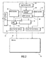
- Fig. 2 shows as a second embodiment a memory device 20 comprising a MRAM 22 and a controller 24.
- the block diagram shown represents the logical structure of the device. A physical implementation of the device may look different than the structure shown here.
- the controller has a memory input port 26 for memory data, a memory output port 28 for write data to be written to MRAM 22, a client input port 30 for address and write data from memory clients such as a CPU, and a client output port 32 for memory data to be communicated to a memory client.
- the memory controller 24 of the embodiment of Fig. 2 has an integrated FIFO register 34 connected to client input port 30.
- a FIFO controller 36 is also connected to FIFO register 34.
- a command decoder 38 is connected to client input port 30, and to a write controller 40 and a read controller 42.
- Interconnected between memory input port 26 and write controller 40 is a XOR-gate 44.
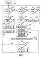
- Fig. 3 Operation of the memory controller 24 will now be described with reference to the flow diagram of Fig. 3 .
- the flow shown in Fig. 3 is not bound to be used in the controller structure of Fig. 2 .
- Any appropriate device can perform the method shown in Fig. 3 .
- the flow can be implemented as software.
- step S12 it is checked whether the request comprises a read command. If this is not the case, command decoder ascertains in step S 14 whether the command is a write command.
- step S14 it may turn out that there is neither a read request nor a write request.
- write controller 40 checks whether the write queue in FIFO register 34 is empty. If this is the case, the method of Fig. 3 arcs back to step S12 to monitor the client input port.
- command decoder 38 forward the request to read controller 42.
- Read controller 42 extracts the address information comprised by the request and forwards it to FIFO controller 36.
- FIFO controller 36 maintains a list of addresses comprised by write requests in the FIFO register. If the address is contained in the list, FIFO controller 44 triggers FIFO 34 to send the corresponding write data to client output port 32.
- FIFO controller 36 returns to read controller 42 that the read request has been served. If the address is not contained in the list, FIFO controller returns this result to read controller 42, which will in turn trigger a read operation from the given address in MRAM 22. MRAM will return the requested data to memory input port 26. The data will from there be forwarded to client output port 32 and sent to the requesting client.
- write controller 42 will first ascertain whether the FIFO register is full. If this is the case, the oldest write request in the queue of FIFO register 34 will be served.
- a write request is served in the present embodiment, deviating in part from the flow of Fig. 3 , in the following way: write controller 40 sends a read request to read controller 42.
- Read controller 42 performs steps S 18 to S22 and returns either data from queue 34 or from memory 22.
- the flow of Fig. 2 shows a simplified version in which data is read directly from the addressed memory sector in a step S30.
- XOR-Gate 44 performs the logical "EXCLUSIVE-OR” operation with the write data and the memory or register data, respectively, in step S32. That is, XOR-Gate 44 will return to write controller 40 a signal, called “mask” herein, which will be a “TRUE” signal ("1") if the data at the inputs of XOR-Gate 44 are different from each other. It will return a "FALSE"-signal if they are identical.
- Write controller 40 will attach the signal from XOR-Gate 44 to the write request and forward the write request to the FIFO register 34. The data will only be written if the mask is "1".
- step S24 In case write controller 44 finds in step S24 that the queue in FIFO register 34 is not full, it will jump to step S30 and perform the partly deviating read routine described above.
- the algorithm can be divided into three parts: Between lines 1 and 9 the read control operation is defined. Between lines 10 and 24 the write control algorithm is defined. Between lines 25 and 37 the control operation in absence of any request is defined.
- the write control can be further subdivided: lines 11 to 19 define the write control operation in the case of a full write queue. Lines 19 to 24 define the write control operation in the alternative case that the write queue is not full.
- the most important commands in the algorithm below are “queue.enqueue” and “mram.write”.
- the first command triggers writing a data field consisting of the write address information ("req.addr"), the write data ("req.data”), that is, e.g., the FIFO register of Fig. 1 or 2 .
- this includes all bits of the write request.
- this includes a "mask” bit indicating the result of the XOR-operation.
- the command "mram.write” will write data included in the command to an MRAM address included in the command, if the mask bit is "1".
Landscapes
- Engineering & Computer Science (AREA)
- Theoretical Computer Science (AREA)
- Physics & Mathematics (AREA)
- General Engineering & Computer Science (AREA)
- General Physics & Mathematics (AREA)
- Static Random-Access Memory (AREA)
- Memory System (AREA)
- Electrophonic Musical Instruments (AREA)
- Communication Control (AREA)
- Techniques For Improving Reliability Of Storages (AREA)
- Saccharide Compounds (AREA)
- Steroid Compounds (AREA)
Claims (23)
- Speichervorrichtung (10, 20) mit einer Speichersteuervorrichtung (14, 24) für einen Speicher (12, 22), der wenigstens eine nichtflüchtige Speicherzelle aufweist, die höhere Kosten für einen Schreibvorgang bedingt als für einen Lesevorgang, indem dem Schreibvorgang eine größere Menge an Energie, Zeit, Leistung, Stromdichte oder Spannung zugeordnet ist als dem Lesevorgang, wobei der Speicherzelle erste Adressinformationen zugeordnet sind und die Speicherzelle dafür ausgelegt ist, Speicherdaten zu Speichern, wobei die Speichersteuervorrichtung umfasst:ein Register (16, 34), das mit dem Speicher verbunden ist und einen Registerraum für Schreibdaten und hierzu zugeordnete Adressinformationen umfasst, undeine Schreibsteuervorrichtung (40), die mit dem Register und dem Speicher verbunden ist, und dafür ausgelegt ist,
eine Schreibanfrage zu empfangen, die die ersten Adressinformationen und erste Schreibdaten umfasst, die hierzu zugeordnet sind,
und in einer ersten Alternative
zu bestimmen, ob die ersten Adressinformationen in dem Register gespeichert sind, und, falls dies zutrifft, die ersten Schreibdaten mit den zweiten Schreibdaten einer früheren Schreibanfrage in dem Register, die den ersten Adressinformationen zugeordnet sind, zu vergleichen, und, falls dies nicht zutrifft, die ersten Schreibdaten mit den Speicherdaten, die den ersten Adressinformationen zugeordnet sind, zu vergleichen
die ersten Adressinformationen und die ersten Schreibdaten jeweils zu dem Register weiterzuleiten, und
eine Schreiboperation für jeweils die ersten oder zweiten Schreibdaten von dem Register in den Speicher zu initiieren, wenn jeweils die ersten oder die zweiten Schreibdaten verschieden von den Speicherdaten sind,
oder in einer zweiten Alternative
die ersten Schreibdaten mit den Speicherdaten, die den ersten Adressinformationen zugeordnet sind, zu vergleichen,
die ersten Adressinformationen und die ersten Schreibdaten zu dem Register weiterzuleiten, wenn die ersten Schreibdaten verschieden von den Speicherdaten sind, und
eine Schreiboperation für die ersten Schreibdaten von dem Register in den Speicher zu initiieren, wenn die ersten Schreibdaten verschieden von den Speicherdaten sind. - Speichervorrichtung (10, 20) nach Anspruch 1, wobei das Register ein FIFO-Register (16, 34) ist.
- Speichervorrichtung (10, 20) nach Anspruch 1 oder 2, wobei die Speichersteuervorrichtung ferner eine Lesesteuervorrichtung (42) umfasst, die mit dem Register und dem Speicher verbunden ist, und dafür ausgelegt ist,
eine Leseanfrage zu empfangen, die die ersten Adressinformationen umfasst,
zu bestimmen, ob die ersten Adressinformationen in dem Register gespeichert sind, und
die Leseanfrage zu dem Register oder dem Speicher weiterzuleiten, in Abhängigkeit davon, ob jeweils die ersten Adressinformationen in dem Register gespeichert sind, oder nicht. - Speichervorrichtung (10, 20) nach Anspruch 3, wobei die Schreibsteuervorrichtung (40) dafür ausgelegt ist, bei Empfang der Schreibanfrage eine Leseanfrage zu der Lesesteuervorrichtung (42) zu Senden, wobei die Leseanfrage die in der Schreibanfrage enthaltenen ersten Adressinformationen umfasst.
- Speichervorrichtung (10, 20) nach Anspruch 1, wobei die Schreibsteuervorrichtung (40) dafür ausgelegt ist,
ein Markierungszeichen zu setzen, das das Ergebnis des Vergleichs mit den ersten Schreibdaten anzeigt, und
das Markierungszeichen zusammen mit den ersten Schreibdaten und den ersten Adressinformationen zu dem Register (16, 34) zu übertragen, und
eine Schreiboperation in den Speicher (22) nur für die ersten Schreibdaten zu initiieren, für die das Markierungszeichen einen Unterschied zwischen den ersten Schreibdaten und jeweils den Speicherdaten oder den zweiten Schreibdaten anzeigt. - Speichervorrichtung (10, 20) nach Anspruch 5, wobei die Schreibsteuervorrichtung (40) dafür ausgelegt ist, zu bestimmen, ob das Register (16, 34) voll oder leer ist.
- Speichervorrichtung (10, 20) nach Anspruch 6, wobei die Schreibsteuervorrichtung (40) dafür ausgelegt ist, wenigstens eine Schreiboperation von dem Register in den Speicher zu initiieren, nachdem festgestellt worden ist, dass das Register voll ist.
- Speichervorrichtung (10, 20) nach Anspruch 1, wobei die Schreibsteuervorrichtung (40) dafür ausgelegt ist, eine Schreiboperation von dem Register in den Speicher zu initiieren, nachdem festgestellt worden ist, dass das Register nicht leer ist, und in dem Fall, in dem keine anhängige Schreibanfrage vorhanden ist.
- Speichervorrichtung (10, 20) nach Anspruch 1, wobei die Schreibsteuervorrichtung (40) dafür ausgelegt ist, den Vergleich der ersten Schreibdaten mit den zweiten Schreibdaten oder dem Speicher für wenigstens ein Bit zu einem Zeitpunkt durchzuführen.
- Speichervorrichtung (10, 20) nach Anspruch 9, wobei die Schreibsteuervorrichtung dafür ausgelegt ist, den Vergleich Byte für Byte oder Bit für Bit durchzuführen.
- Speichervorrichtung (10, 20) nach Anspruch 9, wobei die Schreibsteuervorrichtung dafür ausgelegt ist, den Vergleich Bit für Bit durchzuführen.
- Speichervorrichtung (10, 20) nach Anspruch 9, die ein Exklusiv-ODER-Gatter (44) mit einem ersten Eingang für die ersten Schreibdaten und einem zweiten Eingang für jeweils die Speicherdaten oder die zweiten Schreibdaten, sowie einen Ausgangsanschluss, der mit der Schreibsteuervorrichtung verbunden ist, umfasst.
- Speichervorrichtung (10, 20) nach Anspruch 9, wobei die Schreibsteuervorrichtung (40) dafür ausgelegt ist, die ersten Adressinformationen und die ersten Schreibdaten zu dem Register weiterzuleiten, nachdem wenigstens ein logisches "WAHR"-Signal vom Ausgang des Exklusiv-ODER-Gatters empfangen worden ist.
- Speichervorrichtung (10, 20) nach Anspruch 1, wobei der Speicher Speicherzellen aus der Gruppe bestehend aus MRAM und FERAM umfasst.
- Verfahren zum Schreiben in einen Speicher (12, 22) unter Verwendung einer Schreibwarteschlange (16, 34), wobei der Speicher wenigstens eine nichtflüchtige Speicherzelle zum Speichern von Speicherdaten umfasst, wobei die Speicherzelle eindeutig wenigstens einer ersten Speicheradresse zugeordnet ist und höhere Kosten für einen Schreibvorgang erfordert als für einen Lesevorgang, indem dem Schreibvorgang eine größere Menge an Energie, Zeit, Leistung, Stromdichte oder Spannung zugeordnet ist als dem Lesevorgang, wobei das Verfahren die Schritte umfasst:Empfangen einer Schreibanfrage, die die ersten Adressinformationen und erste Schreibdaten, die hierzu zugeordnet sind, umfasst, undin einer ersten Alternative:Bestimmen, ob die ersten Adressinformationen in der Schreibwarteschlange gespeichert sind, und, falls dies zutrifft, Vergleichen der ersten Schreibdaten mit den zweiten Schreibdaten in der Schreibwarteschlange, die den ersten Adressinformationen zugeordnet sind, und, falls dies nicht zutrifft, Vergleichen der ersten Schreibdaten mit den Speicherdaten, die den ersten Adressinformationen zugeordnet sind (S32),Weiterleiten der ersten Adressinformationen und der ersten Schreibdaten zu der Schreibwarteschlange (16, 34), wenn die ersten Schreibdaten verschieden von jeweils den zweiten Schreibdaten oder den Speicherdaten sind, undSchreiben der ersten Schreibdaten aus der Schreibwarteschlange in die Speicherzelle die der ersten Adresse (S38) entspricht;oder in einer zweiten Alternative:Vergleichen der ersten Schreibdaten mit den Speicherdaten, die den ersten Adressinformationen zugeordnet sind,Weiterleiten der ersten Adressinformationen und der ersten Schreibdaten zu der Schreibwarteschlange, wenn die ersten Schreibdaten verschieden von jeweils den zweiten Schreibdaten oder den Speicherdaten sind, undSchreiben der Schreibdaten von der Schreibwarteschlange in die Speicherzelle entsprechend der ersten Adresse.
- Verfahren nach Anspruch 15, wobei die ersten Schreibdaten von unterschiedlichen Schreibanfragen aus der Schreibwarteschlange entsprechend einer FIFO-Regel geschrieben werden.
- Verfahren nach Anspruch 15, das ferner die Schritte umfasst:Empfangen einer Leseanfrage, die die ersten Adressinformationen umfasst,Bestimmen, ob die ersten Adressinformationen im Register gespeichert sind (S20),Weiterleiten der Leseanfrage zu der Schreibwarteschlange oder zu dem Speicher, in Abhängigkeit davon, ob jeweils die ersten Adressinformationen im Register gespeichert sind, oder nicht (S22),Empfangen der Schreibwarteschlangendaten oder der Speicherdaten, die den ersten Adressinformationen zugeordnet sind, von jeweils der Schreibwarteschlange oder dem Speicher.
- Verfahren nach Anspruch 15, den Schritt umfassend:(S30) Ausführen einer Leseanfrage bei Empfang der Schreibanfrage, wobei die Leseanfrage die ersten Adressinformationen umfasst, die in der Schreibanfrage enthalten sind.
- Verfahren nach Anspruch 15, das den Schritt des Bestimmens umfasst, ob die Schreibwarteschlange voll ist und/oder ob die Schreibwarteschlange leer ist (S24, S16).
- Verfahren nach Anspruch 19, das den Schritt des Schreibens von der Schreibwarteschlange in den Speicher umfasst (S38), nachdem festgestellt worden ist, dass das Register voll ist.
- Verfahren nach Anspruch 19, das einen Schritt des Schreibens von Schreibwarteschlange in den Speicher umfasst (S26), nachdem festgestellt worden ist, dass die Schreibwarteschlange nicht leer ist, und in dem Fall, in dem keine anhängige Schreibanfrage vorhanden ist.
- Verfahren nach Anspruch 15, das den Schritt des Vergleichens wenigstens eines Bits der ersten Schreibdaten und der zweiten Schreibdaten oder der Speicherdaten zu einem Zeitpunkt umfasst (S32, S34).
- Verfahren nach Anspruch 22, wobei der Vergleichsschritt einen Schritt des Ausführens einer Exklusiv-ODER-Operation zwischen den ersten Schreibdaten und jeweils den Speicherdaten oder den zweiten Schreibdaten umfasst (S34).
Priority Applications (1)
| Application Number | Priority Date | Filing Date | Title |
|---|---|---|---|
| EP03813945A EP1581876B1 (de) | 2002-12-30 | 2003-11-26 | Speichersteuerung und verfahren zum schreiben in einen speicher |
Applications Claiming Priority (4)
| Application Number | Priority Date | Filing Date | Title |
|---|---|---|---|
| EP02080598 | 2002-12-30 | ||
| EP02080598 | 2002-12-30 | ||
| PCT/IB2003/005709 WO2004059499A2 (en) | 2002-12-30 | 2003-11-26 | Memory controller and method for writing to a memory |
| EP03813945A EP1581876B1 (de) | 2002-12-30 | 2003-11-26 | Speichersteuerung und verfahren zum schreiben in einen speicher |
Publications (2)
| Publication Number | Publication Date |
|---|---|
| EP1581876A2 EP1581876A2 (de) | 2005-10-05 |
| EP1581876B1 true EP1581876B1 (de) | 2010-08-04 |
Family
ID=32668869
Family Applications (1)
| Application Number | Title | Priority Date | Filing Date |
|---|---|---|---|
| EP03813945A Expired - Lifetime EP1581876B1 (de) | 2002-12-30 | 2003-11-26 | Speichersteuerung und verfahren zum schreiben in einen speicher |
Country Status (8)
| Country | Link |
|---|---|
| US (1) | US7568082B2 (de) |
| EP (1) | EP1581876B1 (de) |
| JP (1) | JP2006512657A (de) |
| CN (1) | CN1732446B (de) |
| AT (1) | ATE476709T1 (de) |
| AU (1) | AU2003303412A1 (de) |
| DE (1) | DE60333677D1 (de) |
| WO (1) | WO2004059499A2 (de) |
Cited By (2)
| Publication number | Priority date | Publication date | Assignee | Title |
|---|---|---|---|---|
| US9268638B2 (en) | 2012-06-06 | 2016-02-23 | Silicon Motion Inc. | Flash memory control method, controller and electronic apparatus |
| TWI594251B (zh) * | 2012-06-06 | 2017-08-01 | 慧榮科技股份有限公司 | 記憶體控制方法、控制器跟電子裝置 |
Families Citing this family (19)
| Publication number | Priority date | Publication date | Assignee | Title |
|---|---|---|---|---|
| US7849253B2 (en) * | 2005-04-04 | 2010-12-07 | Standard Microsystems Corporation | Method for fast access to flash-memory media |
| JP4791909B2 (ja) * | 2006-08-21 | 2011-10-12 | 株式会社東芝 | 高速入出力機能を備える制御装置、及びその制御データの制御方法 |
| JP2008134685A (ja) * | 2006-11-27 | 2008-06-12 | Konica Minolta Business Technologies Inc | 不揮発メモリシステム及び不揮発メモリ制御方法 |
| CN100499557C (zh) * | 2007-06-18 | 2009-06-10 | 中兴通讯股份有限公司 | 一种寻址控制器件及使用该器件进行寻址的方法 |
| US8332575B2 (en) * | 2007-06-20 | 2012-12-11 | Samsung Electronics Co., Ltd. | Data management systems, methods and computer program products using a phase-change random access memory for selective data maintenance |
| TWI391911B (zh) * | 2008-04-15 | 2013-04-01 | Novatek Microelectronics Corp | 記憶體存取裝置及使用該記憶體存取裝置的顯示器 |
| KR101631162B1 (ko) * | 2009-06-11 | 2016-06-17 | 삼성전자주식회사 | 플래시 메모리를 구비하는 저장 장치 및 이의 데이터 저장 방법 |
| CN101876944B (zh) | 2009-11-26 | 2012-02-15 | 威盛电子股份有限公司 | 动态随机存取存储器控制器和控制方法 |
| US8489803B2 (en) * | 2009-12-14 | 2013-07-16 | Smsc Holdings S.A.R.L. | Efficient use of flash memory in flash drives |
| US8806263B2 (en) * | 2011-08-26 | 2014-08-12 | Micron Technology, Inc. | Methods and apparatuses including a global timing generator and local control circuits |
| JP5727948B2 (ja) | 2012-01-16 | 2015-06-03 | 株式会社東芝 | 半導体記憶装置 |
| KR20170048942A (ko) * | 2015-10-27 | 2017-05-10 | 에스케이하이닉스 주식회사 | 반도체장치 및 반도체시스템 |
| US10891057B1 (en) * | 2015-12-31 | 2021-01-12 | EMC IP Holding Company LLC | Optimizing flash device write operations |
| KR102648180B1 (ko) * | 2016-07-19 | 2024-03-18 | 에스케이하이닉스 주식회사 | 메모리 시스템 및 그 동작 방법 |
| CN109426616B (zh) * | 2017-08-31 | 2023-08-04 | 华邦电子股份有限公司 | 字节编程方法以及页面编程方法 |
| CN110457198A (zh) * | 2018-05-07 | 2019-11-15 | 龙芯中科技术有限公司 | 调试信息输出方法、装置及存储介质 |
| US11393550B2 (en) | 2018-09-14 | 2022-07-19 | Rambus Inc. | Memory system with error detection |
| CN112802518B (zh) * | 2021-03-25 | 2021-07-02 | 深圳市汇顶科技股份有限公司 | 数据写入方法、片上系统芯片及计算机可读存储介质 |
| CN114546906B (zh) * | 2022-01-28 | 2023-06-23 | 郑州信大捷安信息技术股份有限公司 | 一种基于ring通信机制的数据交互方法和系统 |
Family Cites Families (13)
| Publication number | Priority date | Publication date | Assignee | Title |
|---|---|---|---|---|
| CN85105547B (zh) * | 1985-07-19 | 1988-06-08 | 株式会社日立制作所 | 用于一信息处理装置的存储器存取控制系统 |
| JPS6379292A (ja) * | 1986-09-24 | 1988-04-09 | Nec Corp | スタテイツク型メモリ |
| US5224214A (en) * | 1990-04-12 | 1993-06-29 | Digital Equipment Corp. | BuIffet for gathering write requests and resolving read conflicts by matching read and write requests |
| US5553265A (en) * | 1994-10-21 | 1996-09-03 | International Business Machines Corporation | Methods and system for merging data during cache checking and write-back cycles for memory reads and writes |
| US5787484A (en) * | 1996-08-08 | 1998-07-28 | Micron Technology, Inc. | System and method which compares data preread from memory cells to data to be written to the cells |
| US5835406A (en) | 1996-10-24 | 1998-11-10 | Micron Quantum Devices, Inc. | Apparatus and method for selecting data bits read from a multistate memory |
| JPH10154394A (ja) | 1996-11-21 | 1998-06-09 | Toshiba Corp | メモリ装置 |
| US6438660B1 (en) * | 1997-12-09 | 2002-08-20 | Intel Corporation | Method and apparatus for collapsing writebacks to a memory for resource efficiency |
| US6151658A (en) * | 1998-01-16 | 2000-11-21 | Advanced Micro Devices, Inc. | Write-buffer FIFO architecture with random access snooping capability |
| JP2001014219A (ja) * | 1999-06-30 | 2001-01-19 | Nec Corp | キャッシュ制御方法及びその装置 |
| US6678838B1 (en) * | 1999-08-23 | 2004-01-13 | Advanced Micro Devices, Inc. | Method to track master contribution information in a write buffer |
| CN1121041C (zh) * | 2000-11-27 | 2003-09-10 | 英业达集团(南京)电子技术有限公司 | 在快闪存储器中同时存放程序代码及数据资料的方法 |
| JP3701886B2 (ja) * | 2001-04-27 | 2005-10-05 | インターナショナル・ビジネス・マシーンズ・コーポレーション | 記憶回路ブロック及びアクセス方法 |
-
2003
- 2003-11-26 DE DE60333677T patent/DE60333677D1/de not_active Expired - Lifetime
- 2003-11-26 CN CN2003801079434A patent/CN1732446B/zh not_active Expired - Fee Related
- 2003-11-26 AU AU2003303412A patent/AU2003303412A1/en not_active Abandoned
- 2003-11-26 JP JP2004563431A patent/JP2006512657A/ja not_active Withdrawn
- 2003-11-26 AT AT03813945T patent/ATE476709T1/de not_active IP Right Cessation
- 2003-11-26 US US10/541,266 patent/US7568082B2/en not_active Expired - Lifetime
- 2003-11-26 WO PCT/IB2003/005709 patent/WO2004059499A2/en not_active Ceased
- 2003-11-26 EP EP03813945A patent/EP1581876B1/de not_active Expired - Lifetime
Cited By (3)
| Publication number | Priority date | Publication date | Assignee | Title |
|---|---|---|---|---|
| US9268638B2 (en) | 2012-06-06 | 2016-02-23 | Silicon Motion Inc. | Flash memory control method, controller and electronic apparatus |
| US9417958B2 (en) | 2012-06-06 | 2016-08-16 | Silicon Motion Inc. | Flash memory control method, controller and electronic apparatus |
| TWI594251B (zh) * | 2012-06-06 | 2017-08-01 | 慧榮科技股份有限公司 | 記憶體控制方法、控制器跟電子裝置 |
Also Published As
| Publication number | Publication date |
|---|---|
| CN1732446A (zh) | 2006-02-08 |
| US20060106969A1 (en) | 2006-05-18 |
| AU2003303412A1 (en) | 2004-07-22 |
| US7568082B2 (en) | 2009-07-28 |
| EP1581876A2 (de) | 2005-10-05 |
| DE60333677D1 (de) | 2010-09-16 |
| JP2006512657A (ja) | 2006-04-13 |
| CN1732446B (zh) | 2010-09-08 |
| WO2004059499A3 (en) | 2004-09-02 |
| ATE476709T1 (de) | 2010-08-15 |
| WO2004059499A2 (en) | 2004-07-15 |
Similar Documents
| Publication | Publication Date | Title |
|---|---|---|
| US7568082B2 (en) | Memory controller and method for writing to a memory | |
| US11636034B2 (en) | Write-back cache policy to limit data transfer time to a memory device | |
| EP1643506B1 (de) | System und Verfahren zum Datensichern bei Stromausfall | |
| US6629211B2 (en) | Method and system for improving raid controller performance through adaptive write back/write through caching | |
| US7886110B2 (en) | Dynamically adjusting cache policy based on device load in a mass storage system | |
| KR102459964B1 (ko) | 가상 메모리 용량을 제공하는 메모리 모듈 및 그것의 동작 방법 | |
| US11188467B2 (en) | Multi-level system memory with near memory capable of storing compressed cache lines | |
| EP0952524A1 (de) | Mehrweg-Cachespeichervorrichtung und Verfahren | |
| EP3382558B1 (de) | Vorrichtung, verfahren und system für rechtzeitige cache-assoziativität | |
| US6243770B1 (en) | Method for determining status of multiple interlocking FIFO buffer structures based on the position of at least one pointer of each of the multiple FIFO buffers | |
| CN107861887A (zh) | 一种串行易失性存储器的控制方法 | |
| US7552307B2 (en) | Method for initializing a random access memory | |
| US7035987B2 (en) | Managing storage in processor-based systems | |
| EP1387277A2 (de) | Nachschreibstrategie für Speicher | |
| US6449690B1 (en) | Caching method using cache data stored in dynamic RAM embedded in logic chip and cache tag stored in static RAM external to logic chip | |
| US10452312B2 (en) | Apparatus, system, and method to determine a demarcation voltage to use to read a non-volatile memory | |
| US7240170B2 (en) | High/low priority memory | |
| US20040024969A1 (en) | Methods and apparatuses for managing memory | |
| US6718451B2 (en) | Utilizing overhead in fixed length memory block pools | |
| US7587556B2 (en) | Store buffer capable of maintaining associated cache information | |
| EP1387278A2 (de) | Verfahren und Vorrichtungen zur Speicherverwaltung | |
| JP2023031010A (ja) | 不揮発性メモリおよびメモリシステム | |
| US6654854B1 (en) | Caching method using cache tag and cache data stored in dynamic RAM embedded in logic chip | |
| EP1387276A2 (de) | Verfahren und Vorrichtung zur Speicherverwaltung | |
| US6920535B1 (en) | Accessing multi-ported memory for uncached status and control accesses |
Legal Events
| Date | Code | Title | Description |
|---|---|---|---|
| PUAI | Public reference made under article 153(3) epc to a published international application that has entered the european phase |
Free format text: ORIGINAL CODE: 0009012 |
|
| 17P | Request for examination filed |
Effective date: 20050801 |
|
| AK | Designated contracting states |
Kind code of ref document: A2 Designated state(s): AT BE BG CH CY CZ DE DK EE ES FI FR GB GR HU IE IT LI LU MC NL PT RO SE SI SK TR |
|
| AX | Request for extension of the european patent |
Extension state: AL LT LV MK |
|
| DAX | Request for extension of the european patent (deleted) | ||
| 17Q | First examination report despatched |
Effective date: 20061010 |
|
| RAP1 | Party data changed (applicant data changed or rights of an application transferred) |
Owner name: NXP B.V. |
|
| GRAP | Despatch of communication of intention to grant a patent |
Free format text: ORIGINAL CODE: EPIDOSNIGR1 |
|
| GRAS | Grant fee paid |
Free format text: ORIGINAL CODE: EPIDOSNIGR3 |
|
| GRAA | (expected) grant |
Free format text: ORIGINAL CODE: 0009210 |
|
| AK | Designated contracting states |
Kind code of ref document: B1 Designated state(s): AT BE BG CH CY CZ DE DK EE ES FI FR GB GR HU IE IT LI LU MC NL PT RO SE SI SK TR |
|
| REG | Reference to a national code |
Ref country code: GB Ref legal event code: FG4D |
|
| REG | Reference to a national code |
Ref country code: CH Ref legal event code: EP |
|
| REG | Reference to a national code |
Ref country code: IE Ref legal event code: FG4D |
|
| REF | Corresponds to: |
Ref document number: 60333677 Country of ref document: DE Date of ref document: 20100916 Kind code of ref document: P |
|
| REG | Reference to a national code |
Ref country code: NL Ref legal event code: VDEP Effective date: 20100804 |
|
| PG25 | Lapsed in a contracting state [announced via postgrant information from national office to epo] |
Ref country code: AT Free format text: LAPSE BECAUSE OF FAILURE TO SUBMIT A TRANSLATION OF THE DESCRIPTION OR TO PAY THE FEE WITHIN THE PRESCRIBED TIME-LIMIT Effective date: 20100804 Ref country code: FI Free format text: LAPSE BECAUSE OF FAILURE TO SUBMIT A TRANSLATION OF THE DESCRIPTION OR TO PAY THE FEE WITHIN THE PRESCRIBED TIME-LIMIT Effective date: 20100804 Ref country code: NL Free format text: LAPSE BECAUSE OF FAILURE TO SUBMIT A TRANSLATION OF THE DESCRIPTION OR TO PAY THE FEE WITHIN THE PRESCRIBED TIME-LIMIT Effective date: 20100804 |
|
| PG25 | Lapsed in a contracting state [announced via postgrant information from national office to epo] |
Ref country code: SI Free format text: LAPSE BECAUSE OF FAILURE TO SUBMIT A TRANSLATION OF THE DESCRIPTION OR TO PAY THE FEE WITHIN THE PRESCRIBED TIME-LIMIT Effective date: 20100804 Ref country code: CY Free format text: LAPSE BECAUSE OF FAILURE TO SUBMIT A TRANSLATION OF THE DESCRIPTION OR TO PAY THE FEE WITHIN THE PRESCRIBED TIME-LIMIT Effective date: 20100804 Ref country code: PT Free format text: LAPSE BECAUSE OF FAILURE TO SUBMIT A TRANSLATION OF THE DESCRIPTION OR TO PAY THE FEE WITHIN THE PRESCRIBED TIME-LIMIT Effective date: 20101206 Ref country code: BG Free format text: LAPSE BECAUSE OF FAILURE TO SUBMIT A TRANSLATION OF THE DESCRIPTION OR TO PAY THE FEE WITHIN THE PRESCRIBED TIME-LIMIT Effective date: 20101104 |
|
| PG25 | Lapsed in a contracting state [announced via postgrant information from national office to epo] |
Ref country code: GR Free format text: LAPSE BECAUSE OF FAILURE TO SUBMIT A TRANSLATION OF THE DESCRIPTION OR TO PAY THE FEE WITHIN THE PRESCRIBED TIME-LIMIT Effective date: 20101105 Ref country code: BE Free format text: LAPSE BECAUSE OF FAILURE TO SUBMIT A TRANSLATION OF THE DESCRIPTION OR TO PAY THE FEE WITHIN THE PRESCRIBED TIME-LIMIT Effective date: 20100804 Ref country code: SE Free format text: LAPSE BECAUSE OF FAILURE TO SUBMIT A TRANSLATION OF THE DESCRIPTION OR TO PAY THE FEE WITHIN THE PRESCRIBED TIME-LIMIT Effective date: 20100804 |
|
| PG25 | Lapsed in a contracting state [announced via postgrant information from national office to epo] |
Ref country code: DK Free format text: LAPSE BECAUSE OF FAILURE TO SUBMIT A TRANSLATION OF THE DESCRIPTION OR TO PAY THE FEE WITHIN THE PRESCRIBED TIME-LIMIT Effective date: 20100804 |
|
| PG25 | Lapsed in a contracting state [announced via postgrant information from national office to epo] |
Ref country code: CZ Free format text: LAPSE BECAUSE OF FAILURE TO SUBMIT A TRANSLATION OF THE DESCRIPTION OR TO PAY THE FEE WITHIN THE PRESCRIBED TIME-LIMIT Effective date: 20100804 Ref country code: SK Free format text: LAPSE BECAUSE OF FAILURE TO SUBMIT A TRANSLATION OF THE DESCRIPTION OR TO PAY THE FEE WITHIN THE PRESCRIBED TIME-LIMIT Effective date: 20100804 Ref country code: IT Free format text: LAPSE BECAUSE OF FAILURE TO SUBMIT A TRANSLATION OF THE DESCRIPTION OR TO PAY THE FEE WITHIN THE PRESCRIBED TIME-LIMIT Effective date: 20100804 Ref country code: EE Free format text: LAPSE BECAUSE OF FAILURE TO SUBMIT A TRANSLATION OF THE DESCRIPTION OR TO PAY THE FEE WITHIN THE PRESCRIBED TIME-LIMIT Effective date: 20100804 Ref country code: RO Free format text: LAPSE BECAUSE OF FAILURE TO SUBMIT A TRANSLATION OF THE DESCRIPTION OR TO PAY THE FEE WITHIN THE PRESCRIBED TIME-LIMIT Effective date: 20100804 |
|
| PLBE | No opposition filed within time limit |
Free format text: ORIGINAL CODE: 0009261 |
|
| STAA | Information on the status of an ep patent application or granted ep patent |
Free format text: STATUS: NO OPPOSITION FILED WITHIN TIME LIMIT |
|
| PG25 | Lapsed in a contracting state [announced via postgrant information from national office to epo] |
Ref country code: ES Free format text: LAPSE BECAUSE OF FAILURE TO SUBMIT A TRANSLATION OF THE DESCRIPTION OR TO PAY THE FEE WITHIN THE PRESCRIBED TIME-LIMIT Effective date: 20101115 Ref country code: MC Free format text: LAPSE BECAUSE OF NON-PAYMENT OF DUE FEES Effective date: 20101130 |
|
| REG | Reference to a national code |
Ref country code: CH Ref legal event code: PL |
|
| 26N | No opposition filed |
Effective date: 20110506 |
|
| PG25 | Lapsed in a contracting state [announced via postgrant information from national office to epo] |
Ref country code: LI Free format text: LAPSE BECAUSE OF NON-PAYMENT OF DUE FEES Effective date: 20101130 Ref country code: CH Free format text: LAPSE BECAUSE OF NON-PAYMENT OF DUE FEES Effective date: 20101130 |
|
| REG | Reference to a national code |
Ref country code: DE Ref legal event code: R097 Ref document number: 60333677 Country of ref document: DE Effective date: 20110506 |
|
| PG25 | Lapsed in a contracting state [announced via postgrant information from national office to epo] |
Ref country code: IE Free format text: LAPSE BECAUSE OF NON-PAYMENT OF DUE FEES Effective date: 20101126 |
|
| REG | Reference to a national code |
Ref country code: GB Ref legal event code: 732E Free format text: REGISTERED BETWEEN 20120510 AND 20120516 |
|
| REG | Reference to a national code |
Ref country code: DE Ref legal event code: R081 Ref document number: 60333677 Country of ref document: DE Owner name: CROCUS TECHNOLOGY,INC.(N.D.GES.D.STAATES DELAW, US Free format text: FORMER OWNER: NXP B.V., EINDHOVEN, NL Effective date: 20120419 |
|
| PG25 | Lapsed in a contracting state [announced via postgrant information from national office to epo] |
Ref country code: LU Free format text: LAPSE BECAUSE OF NON-PAYMENT OF DUE FEES Effective date: 20101126 Ref country code: HU Free format text: LAPSE BECAUSE OF FAILURE TO SUBMIT A TRANSLATION OF THE DESCRIPTION OR TO PAY THE FEE WITHIN THE PRESCRIBED TIME-LIMIT Effective date: 20110205 |
|
| PG25 | Lapsed in a contracting state [announced via postgrant information from national office to epo] |
Ref country code: TR Free format text: LAPSE BECAUSE OF FAILURE TO SUBMIT A TRANSLATION OF THE DESCRIPTION OR TO PAY THE FEE WITHIN THE PRESCRIBED TIME-LIMIT Effective date: 20100804 |
|
| REG | Reference to a national code |
Ref country code: FR Ref legal event code: PLFP Year of fee payment: 13 |
|
| REG | Reference to a national code |
Ref country code: FR Ref legal event code: PLFP Year of fee payment: 14 |
|
| REG | Reference to a national code |
Ref country code: FR Ref legal event code: PLFP Year of fee payment: 15 |
|
| REG | Reference to a national code |
Ref country code: FR Ref legal event code: TP Owner name: CROCUS TECHNOLOGY INC., US Effective date: 20171221 |
|
| REG | Reference to a national code |
Ref country code: FR Ref legal event code: CA Effective date: 20180522 |
|
| REG | Reference to a national code |
Ref country code: FR Ref legal event code: PLFP Year of fee payment: 16 |
|
| PGFP | Annual fee paid to national office [announced via postgrant information from national office to epo] |
Ref country code: FR Payment date: 20221021 Year of fee payment: 20 |
|
| PGFP | Annual fee paid to national office [announced via postgrant information from national office to epo] |
Ref country code: GB Payment date: 20221021 Year of fee payment: 20 Ref country code: DE Payment date: 20221020 Year of fee payment: 20 |
|
| P01 | Opt-out of the competence of the unified patent court (upc) registered |
Effective date: 20230626 |
|
| REG | Reference to a national code |
Ref country code: DE Ref legal event code: R071 Ref document number: 60333677 Country of ref document: DE |
|
| REG | Reference to a national code |
Ref country code: GB Ref legal event code: PE20 Expiry date: 20231125 |
|
| PG25 | Lapsed in a contracting state [announced via postgrant information from national office to epo] |
Ref country code: GB Free format text: LAPSE BECAUSE OF EXPIRATION OF PROTECTION Effective date: 20231125 |
|
| PG25 | Lapsed in a contracting state [announced via postgrant information from national office to epo] |
Ref country code: GB Free format text: LAPSE BECAUSE OF EXPIRATION OF PROTECTION Effective date: 20231125 |