EP1585095A2 - Verfahren und Einrichtung zum Steuern einer Anzeigetafel - Google Patents
Verfahren und Einrichtung zum Steuern einer Anzeigetafel Download PDFInfo
- Publication number
- EP1585095A2 EP1585095A2 EP05075346A EP05075346A EP1585095A2 EP 1585095 A2 EP1585095 A2 EP 1585095A2 EP 05075346 A EP05075346 A EP 05075346A EP 05075346 A EP05075346 A EP 05075346A EP 1585095 A2 EP1585095 A2 EP 1585095A2
- Authority
- EP
- European Patent Office
- Prior art keywords
- low level
- scanning
- sustain
- period
- high level
- Prior art date
- Legal status (The legal status is an assumption and is not a legal conclusion. Google has not performed a legal analysis and makes no representation as to the accuracy of the status listed.)
- Withdrawn
Links
Images




Classifications
-
- G—PHYSICS
- G09—EDUCATION; CRYPTOGRAPHY; DISPLAY; ADVERTISING; SEALS
- G09G—ARRANGEMENTS OR CIRCUITS FOR CONTROL OF INDICATING DEVICES USING STATIC MEANS TO PRESENT VARIABLE INFORMATION
- G09G3/00—Control arrangements or circuits, of interest only in connection with visual indicators other than cathode-ray tubes
- G09G3/20—Control arrangements or circuits, of interest only in connection with visual indicators other than cathode-ray tubes for presentation of an assembly of a number of characters, e.g. a page, by composing the assembly by combination of individual elements arranged in a matrix no fixed position being assigned to or needed to be assigned to the individual characters or partial characters
- G09G3/22—Control arrangements or circuits, of interest only in connection with visual indicators other than cathode-ray tubes for presentation of an assembly of a number of characters, e.g. a page, by composing the assembly by combination of individual elements arranged in a matrix no fixed position being assigned to or needed to be assigned to the individual characters or partial characters using controlled light sources
- G09G3/28—Control arrangements or circuits, of interest only in connection with visual indicators other than cathode-ray tubes for presentation of an assembly of a number of characters, e.g. a page, by composing the assembly by combination of individual elements arranged in a matrix no fixed position being assigned to or needed to be assigned to the individual characters or partial characters using controlled light sources using luminous gas-discharge panels, e.g. plasma panels
- G09G3/288—Control arrangements or circuits, of interest only in connection with visual indicators other than cathode-ray tubes for presentation of an assembly of a number of characters, e.g. a page, by composing the assembly by combination of individual elements arranged in a matrix no fixed position being assigned to or needed to be assigned to the individual characters or partial characters using controlled light sources using luminous gas-discharge panels, e.g. plasma panels using AC panels
- G09G3/296—Driving circuits for producing the waveforms applied to the driving electrodes
-
- G—PHYSICS
- G09—EDUCATION; CRYPTOGRAPHY; DISPLAY; ADVERTISING; SEALS
- G09G—ARRANGEMENTS OR CIRCUITS FOR CONTROL OF INDICATING DEVICES USING STATIC MEANS TO PRESENT VARIABLE INFORMATION
- G09G3/00—Control arrangements or circuits, of interest only in connection with visual indicators other than cathode-ray tubes
- G09G3/20—Control arrangements or circuits, of interest only in connection with visual indicators other than cathode-ray tubes for presentation of an assembly of a number of characters, e.g. a page, by composing the assembly by combination of individual elements arranged in a matrix no fixed position being assigned to or needed to be assigned to the individual characters or partial characters
- G09G3/22—Control arrangements or circuits, of interest only in connection with visual indicators other than cathode-ray tubes for presentation of an assembly of a number of characters, e.g. a page, by composing the assembly by combination of individual elements arranged in a matrix no fixed position being assigned to or needed to be assigned to the individual characters or partial characters using controlled light sources
- G09G3/28—Control arrangements or circuits, of interest only in connection with visual indicators other than cathode-ray tubes for presentation of an assembly of a number of characters, e.g. a page, by composing the assembly by combination of individual elements arranged in a matrix no fixed position being assigned to or needed to be assigned to the individual characters or partial characters using controlled light sources using luminous gas-discharge panels, e.g. plasma panels
- G09G3/288—Control arrangements or circuits, of interest only in connection with visual indicators other than cathode-ray tubes for presentation of an assembly of a number of characters, e.g. a page, by composing the assembly by combination of individual elements arranged in a matrix no fixed position being assigned to or needed to be assigned to the individual characters or partial characters using controlled light sources using luminous gas-discharge panels, e.g. plasma panels using AC panels
- G09G3/291—Control arrangements or circuits, of interest only in connection with visual indicators other than cathode-ray tubes for presentation of an assembly of a number of characters, e.g. a page, by composing the assembly by combination of individual elements arranged in a matrix no fixed position being assigned to or needed to be assigned to the individual characters or partial characters using controlled light sources using luminous gas-discharge panels, e.g. plasma panels using AC panels controlling the gas discharge to control a cell condition, e.g. by means of specific pulse shapes
- G09G3/294—Control arrangements or circuits, of interest only in connection with visual indicators other than cathode-ray tubes for presentation of an assembly of a number of characters, e.g. a page, by composing the assembly by combination of individual elements arranged in a matrix no fixed position being assigned to or needed to be assigned to the individual characters or partial characters using controlled light sources using luminous gas-discharge panels, e.g. plasma panels using AC panels controlling the gas discharge to control a cell condition, e.g. by means of specific pulse shapes for lighting or sustain discharge
-
- G—PHYSICS
- G09—EDUCATION; CRYPTOGRAPHY; DISPLAY; ADVERTISING; SEALS
- G09G—ARRANGEMENTS OR CIRCUITS FOR CONTROL OF INDICATING DEVICES USING STATIC MEANS TO PRESENT VARIABLE INFORMATION
- G09G2310/00—Command of the display device
- G09G2310/02—Addressing, scanning or driving the display screen or processing steps related thereto
- G09G2310/0202—Addressing of scan or signal lines
- G09G2310/0216—Interleaved control phases for different scan lines in the same sub-field, e.g. initialization, addressing and sustaining in plasma displays that are not simultaneous for all scan lines
-
- G—PHYSICS
- G09—EDUCATION; CRYPTOGRAPHY; DISPLAY; ADVERTISING; SEALS
- G09G—ARRANGEMENTS OR CIRCUITS FOR CONTROL OF INDICATING DEVICES USING STATIC MEANS TO PRESENT VARIABLE INFORMATION
- G09G2310/00—Command of the display device
- G09G2310/02—Addressing, scanning or driving the display screen or processing steps related thereto
- G09G2310/0202—Addressing of scan or signal lines
- G09G2310/0218—Addressing of scan or signal lines with collection of electrodes in groups for n-dimensional addressing
-
- G—PHYSICS
- G09—EDUCATION; CRYPTOGRAPHY; DISPLAY; ADVERTISING; SEALS
- G09G—ARRANGEMENTS OR CIRCUITS FOR CONTROL OF INDICATING DEVICES USING STATIC MEANS TO PRESENT VARIABLE INFORMATION
- G09G2320/00—Control of display operating conditions
- G09G2320/02—Improving the quality of display appearance
- G09G2320/0228—Increasing the driving margin in plasma displays
-
- G—PHYSICS
- G09—EDUCATION; CRYPTOGRAPHY; DISPLAY; ADVERTISING; SEALS
- G09G—ARRANGEMENTS OR CIRCUITS FOR CONTROL OF INDICATING DEVICES USING STATIC MEANS TO PRESENT VARIABLE INFORMATION
- G09G2330/00—Aspects of power supply; Aspects of display protection and defect management
- G09G2330/02—Details of power systems and of start or stop of display operation
- G09G2330/028—Generation of voltages supplied to electrode drivers in a matrix display other than LCD
-
- G—PHYSICS
- G09—EDUCATION; CRYPTOGRAPHY; DISPLAY; ADVERTISING; SEALS
- G09G—ARRANGEMENTS OR CIRCUITS FOR CONTROL OF INDICATING DEVICES USING STATIC MEANS TO PRESENT VARIABLE INFORMATION
- G09G3/00—Control arrangements or circuits, of interest only in connection with visual indicators other than cathode-ray tubes
- G09G3/20—Control arrangements or circuits, of interest only in connection with visual indicators other than cathode-ray tubes for presentation of an assembly of a number of characters, e.g. a page, by composing the assembly by combination of individual elements arranged in a matrix no fixed position being assigned to or needed to be assigned to the individual characters or partial characters
- G09G3/2007—Display of intermediate tones
- G09G3/2018—Display of intermediate tones by time modulation using two or more time intervals
- G09G3/2022—Display of intermediate tones by time modulation using two or more time intervals using sub-frames
-
- G—PHYSICS
- G09—EDUCATION; CRYPTOGRAPHY; DISPLAY; ADVERTISING; SEALS
- G09G—ARRANGEMENTS OR CIRCUITS FOR CONTROL OF INDICATING DEVICES USING STATIC MEANS TO PRESENT VARIABLE INFORMATION
- G09G3/00—Control arrangements or circuits, of interest only in connection with visual indicators other than cathode-ray tubes
- G09G3/20—Control arrangements or circuits, of interest only in connection with visual indicators other than cathode-ray tubes for presentation of an assembly of a number of characters, e.g. a page, by composing the assembly by combination of individual elements arranged in a matrix no fixed position being assigned to or needed to be assigned to the individual characters or partial characters
- G09G3/22—Control arrangements or circuits, of interest only in connection with visual indicators other than cathode-ray tubes for presentation of an assembly of a number of characters, e.g. a page, by composing the assembly by combination of individual elements arranged in a matrix no fixed position being assigned to or needed to be assigned to the individual characters or partial characters using controlled light sources
- G09G3/28—Control arrangements or circuits, of interest only in connection with visual indicators other than cathode-ray tubes for presentation of an assembly of a number of characters, e.g. a page, by composing the assembly by combination of individual elements arranged in a matrix no fixed position being assigned to or needed to be assigned to the individual characters or partial characters using controlled light sources using luminous gas-discharge panels, e.g. plasma panels
- G09G3/288—Control arrangements or circuits, of interest only in connection with visual indicators other than cathode-ray tubes for presentation of an assembly of a number of characters, e.g. a page, by composing the assembly by combination of individual elements arranged in a matrix no fixed position being assigned to or needed to be assigned to the individual characters or partial characters using controlled light sources using luminous gas-discharge panels, e.g. plasma panels using AC panels
- G09G3/291—Control arrangements or circuits, of interest only in connection with visual indicators other than cathode-ray tubes for presentation of an assembly of a number of characters, e.g. a page, by composing the assembly by combination of individual elements arranged in a matrix no fixed position being assigned to or needed to be assigned to the individual characters or partial characters using controlled light sources using luminous gas-discharge panels, e.g. plasma panels using AC panels controlling the gas discharge to control a cell condition, e.g. by means of specific pulse shapes
- G09G3/294—Control arrangements or circuits, of interest only in connection with visual indicators other than cathode-ray tubes for presentation of an assembly of a number of characters, e.g. a page, by composing the assembly by combination of individual elements arranged in a matrix no fixed position being assigned to or needed to be assigned to the individual characters or partial characters using controlled light sources using luminous gas-discharge panels, e.g. plasma panels using AC panels controlling the gas discharge to control a cell condition, e.g. by means of specific pulse shapes for lighting or sustain discharge
- G09G3/2948—Control arrangements or circuits, of interest only in connection with visual indicators other than cathode-ray tubes for presentation of an assembly of a number of characters, e.g. a page, by composing the assembly by combination of individual elements arranged in a matrix no fixed position being assigned to or needed to be assigned to the individual characters or partial characters using controlled light sources using luminous gas-discharge panels, e.g. plasma panels using AC panels controlling the gas discharge to control a cell condition, e.g. by means of specific pulse shapes for lighting or sustain discharge by increasing the total sustaining time with respect to other times in the frame
Definitions
- the present invention relates to a display panel, such as a plasma display panel (PDP), which displays an image by sequentially using an address period and a sustain period, and more particularly, to a display panel driving method and apparatus which group display cells into a plurality of groups and drive each of the groups individually.
- a display panel such as a plasma display panel (PDP)
- PDP plasma display panel
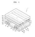
- FIG. 1 shows a structure of a conventional plasma display panel 1 with a 3-electrode surface discharge structure.
- the address electrode lines A 1 , A 2 , ..., A m are formed in a predetermined pattern on an upper surface of the rear glass substrate 106.
- the lower dielectric layer 110 covers the address electrode lines A 1 , A 2 , ..., A m .
- the partition walls 114 are formed on the surface of the lower dielectric layer 110 and parallel to the address electrode lines A 1 , A 2 , ..., A m .
- the partition walls 114 partition discharge areas of display cells and prevent optical interference between the display cells.
- the phosphor layers 112 are formed between each pair of adjacent partition walls 114.
- the X electrode lines X 1 , ..., X n and the Y electrode lines Y 1 , ..., Y n , constituting display electrode line pairs are formed in a predetermined pattern on a lower surface of the front glass substrate 100 in such a way as to intersect the address electrode lines A 1 , A 2 , ..., A m . Each of the intersections forms a corresponding display cell.
- Each of the X-electrode lines X 1 , ..., X n and each of the Y-electrode lines Y 1 ..., Y n are formed by coupling transparent electrode lines X na and Y na , composed of a transparent conductive material such as ITO (Indium Tin Oxide) with metal electrode lines X nb and Y nb for enhancing conductivity.
- the upper dielectric layer 102 covers the X-electrode lines X 1 ,..., X n and the Y electrode lines Y 1 , ..., Y n .
- a protection layer 104 for protecting the panel I in a strong electric field, such as a MgO layer, is formed on the rear surface of the upper dielectric layer 102.
- a discharge space 108 is filled with plasma-forming gas and is sealed up.
- an initialization period, an address period, and a display sustain period are sequentially used in a unit sub-field.
- the initialization period is required to uniformly distribute electric charges in all display cells to be driven.
- a charge state of display cells to be selected and a charge state of display cells not to be selected are set.
- a display discharge is carried out in the display cells to be selected.
- plasma is generated by plasma-forming gas in the display cells being subjected to the display discharge, and the phosphors 112 of the display cells are excited by ultraviolet emission from the plasma, thereby emitting a light.
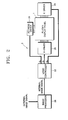
- FIG. 2 is a block diagram of a conventional driving apparatus for driving the conventional plasma display panel of FIG. 1.
- the conventional driving apparatus of the plasma display panel 1 includes an image processor 200, a controller 202, an address driving unit 206, a X driver 208, and a Y driver 204.
- the image processor 200 converts external analog image signals into digital signals and generates internal image signals, such as, for example, red (R), green (G), and blue (B) image signals.
- the image signals each have 8 bits, clock signals, and vertical and horizontal synchronization signals.
- the controller 202 generates driving control signals S A , S Y , and S X in response to the internal image signals received from the image processor 200.
- the address driver 206 receives and processes the address signal S A among the driving control signals S A , S Y , and S X output from the controller 202, generates a display data signal, and transmits the display data signal to address electrode lines.
- the X driver 208 receives and processes the X driving control signal S X among the driving control signals S A , S Y , and S X output from the controller 202 and transmits the X driving control signal S X to X electrode lines.
- the Y driver 204 receives and processes the Y driving control signal S Y among the driving control signals S A , S Y , and S X output from the controller 202 and transmits the Y driving control signal S Y to Y electrode lines.
- a method for driving the plasma display panel 1 with the above-described structure is disclosed in U.S. Patent No. 5,541,618 describing an Address-Display Separation (ADS) driving method.
- ADS Address-Display Separation
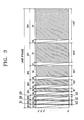
- FIG. 3 is a view for explaining the conventional ADS driving method applied to Y electrode lines of the conventional plasma display panel of FIG. 1.
- a unit frame is divided into a predetermined number of sub-fields, such as, for example, 8 sub-fields SF1 through SF8, for time-division gray-scale display.
- the sub-fields SF1, ..., SF8 are divided into resetting periods (not shown), addressing periods A1, ..., A8, and discharge sustain periods S 1, ..., S8, respectively.
- corresponding scanning pulses are sequentially transmitted to the respective Y electrode lines Y 1 , ..., Y n , while a display data signal is transmitted to the respective address electrode lines (A 1 , A 2 , ... , A m of FIG. 1).
- discharge sustain pulses are transmitted alternately to all the Y electrode lines Y 1 , ..., Y n and all the X electrode lines X 1 , ..., X n , thus generating a display discharge in discharge cells that wall charges are formed in during the corresponding addressing periods A1, ..., A8.
- brightness of a plasma display panel is proportional to the number of total sustain discharge pulses within the discharge sustain periods S1, ..., S8 included in a unit frame. If a frame forming an image consists of 8 sub-fields with 256 gray-scales, different sustain pulse numbers of 1, 2, 4, 8, 16, 32, 64 and 128 can be allocated to the respective subfields in this order. In this case, in order to obtain brightness with 133 gray-scales, it is needed to address and sustain-discharge cells during a first sub-field period SF1, a third sub-field period SF3, and an eighth sub-field period SF8.
- the number of the sustain pulses allocated to each of the sub-fields can be set according to weight values of sub-fields on the basis of APC (Automatic Power Control). Also, the number of the discharge sustain pulses allocated to each of the sub-fields can be changed variously in consideration of gamma characteristics and/or panel characteristics. For example, decreasing a gray-scale allocated to the fourth sub-field SF4 from 8 to 6 and increasing a gray-scale allocated to the sixth sub-field SF6 from 32 to 34 is possible. Also, the number of subfields forming a frame can be changed variously according to a design rule.
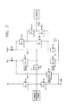
- FIG. 4 is and example of a timing diagram of driving signals used in the conventional plasma display panel of FIG. 1.
- the driving signals are applied to an address electrode A, a command electrode X and scanning electrodes Y 1 through Y n , within a sub-field SF, according to the ADS driving method of an AC PDP.
- the sub-field SF includes a reset period PR, an address period PA and a sustain discharge period PS.
- the reset period PR a reset pulse is applied to all scanning line groups to perform a compulsory write discharge, so that wall charges in entire cells are distributed uniformly. Since the reset period PR is provided prior to the address period PA and is performed throughout an entire screen, it is possible to form wall charges in a very uniform distribution. Therefore, the wall charges in all the cells initialized in the reset period PR are maintained under a similar condition.
- the address period PA starts.
- a bias voltage Ve is applied to the common electrode X to simultaneously turn on scanning electrodes Y 1 through Y n and address electrodes A 1 through A m including cells to be displayed, thereby selecting display cells.
- the sustain discharge period PS starts.
- a sustain pulse V S is applied alternately to the common electrode X and the scanning electrodes Y 1 through Y n , and a voltage V G (for example, ground voltage) with a low level is applied to the address electrodes A 1 through A m .
- Brightness of the PDP is controlled according to the number of the sustain discharge pulses. As the number of the sustain discharge pulses included in a sub-field or in a TV field increases, the brightness of the PDP becomes higher.
- the high level and low level of the sustain discharge signal which are applied alternately to the scanning electrodes and the common electrode in the sustain period PS, are fixed to predetermined values.
- separate driving circuits for each of the groups are required, which increases equipment cost.
- the above-described ADS driving method performs a sustain discharge operation for all the cells of the corresponding scanning electrodes Y 1 through Y n at the same time after terminating addressing of all the first through final scanning electrodes Y 1 through Y n .
- a sustain discharge operation of the corresponding scanning line is performed after an addressing operation of a final scanning line is performed. Accordingly, a larger temporal gap is generated until a sustain discharge operation is performed in cells subjected to the addressing operation, which may make the sustain discharge operation unstable.
- the present invention provides a display panel driving method which groups display cells into a plurality of groups and drives each of the groups individually without an additional driving circuit.
- the present invention also provides a display panel driving method which groups display cells into a plurality of groups and drives each of the groups individually without an additional driving circuit, in order to achieve stable sustain discharge by minimizing a temporal gap between an addressing period and a sustain period in implementing gray-scale.
- the present invention also provides a display panel driving apparatus for performing the display panel driving method.
- a display panel driving method which includes grouping display cells included in scanning electrodes and common electrodes into a plurality of groups, and dividing and driving a frame into a plurality of sub-fields for each group, wherein, each of the plurality of sub-fields includes an address period and a sustain period. Further, in the address period, cells to be displayed are selected, and in the sustain period, high levels and low levels of a sustain discharge signal are applied alternately to the scanning electrodes and the common electrodes so to perform a sustain discharge.
- high level potentials of the sustain discharge signal applied to the scanning electrode are the same in all the groups and the high level potentials of the sustain discharge signal are applied at the same time to all the groups; low level potentials of the sustain discharge signal applied to the scanning electrodes include a first low level potential and a second low level potential higher than the first low level potential.
- a display panel driving method which includes grouping display cells included in scanning electrodes and common electrodes into a plurality of groups, and dividing a frame into a plurality of sub-fields for each group, wherein, each of the plurality of sub-fields includes an address period and a sustain period.
- the address period and the sustain period are performed sequentially to each group in a manner that: a) addressing of each the group is performed and then the sustain period is performed in cells of each the group subjected to addressing; b) addressing of cells of a different group is performed after the sustain period ends; and c) the sustain period is performed selectively in the cells of the different group subjected to addressing while the sustain period is performed in cells of a group.
- high level potentials of the sustain discharge signal applied to the scanning electrode are the same in all the groups and the high level potentials of the sustain discharge signal are applied at the same time to all the groups; low level potentials of the sustain discharge signal applied to the scanning electrodes include a first low level potential and a second low level potential higher than the first low level potential.
- a display panel driving apparatus which applies a scanning signal and a sustain discharge signal to a scanning electrode line of a display panel.
- the apparatus including: a first node, a sustain driving unit, which is connected to the first node, a scanning signal high level applying unit, which is connected to the first node, and a scanning signal low level applying unit, which is connected to the first node.
- a first switch whose one end is connected to the scanning signal high level applying unit; a second low level applying unit, which applies a second low level of a sustain discharge signal; a second switch, which is connected between the other end of the first switch and the second low level applying unit; a high level scanning switch, which is connected between the other end of the first switch and the scanning electrode line; and a low level scanning switch, which is connected between the scanning electrode line and the scanning signal low level applying unit.
- a computer-readable medium having embodied thereon a computer program for executing a display panel driving method
- the medium includes code for grouping display cells included in scanning electrodes and common electrodes into a plurality of groups, code for dividing and driving a frame into a plurality of sub-fields for each group, wherein, each of the plurality of sub-fields includes an address period and a sustain period, code for, in the address period, selecting cells to be displayed. and code for, in the sustain period, applying high levels and low levels of a sustain discharge signal alternately to the scanning electrodes and the common electrodes so to perform a sustain discharge.
- the high level potentials of the sustain discharge signal applied to the scanning electrode are the same in all the groups and the high level potentials of the sustain discharge signal are applied at the same time to all the groups, low level potentials of the sustain discharge signal applied to the scanning electrodes include a first low level potential and a second low level potential higher than the first low level potential.
- An additional exemplary embodiment of the invention provides a computer-readable medium having embodied thereon a computer program for executing a display panel driving method, where the medium includes code for grouping display cells included in scanning electrodes and common electrodes into a plurality of groups, and code for dividing a frame into a plurality of sub-fields for each group, wherein each of the plurality of sub-fields includes an address period and a sustain period.
- the medium includes code for, in at least one of the plurality of sub-fields, sequentially performing the address period and the sustain period to each group in a manner that a) addressing of each the group is performed and then the sustain period is performed in cells of each the group subjected to addressing, b) addressing of cells of a different group is performed after the sustain period ends, and c) the sustain period is performed selectively in the cells of the different group subjected to addressing while the sustain period is performed in cells of a group.
- high level potentials of the sustain discharge signal applied to the scanning electrode are the same in all the groups and the high level potentials of the sustain discharge signal are applied at the same time to all the groups, low level potentials of the sustain discharge signal applied to the scanning electrodes include a first low level potential and a second low level potential higher than the first low level potential.
- a display panel driving method includes driving a frame into a plurality of sub-fields, wherein each of the plurality of sub-fields includes an address period and a sustain period, in the address period, selecting cells to be displayed, and in the sustain period, applying high levels and low levels of a sustain discharge signal alternately to scanning electrodes and common electrodes so to perform a sustain discharge, wherein in at least one sustain period, the high level potentials of the sustain discharge signal applied to the scanning electrode are the same and the high level potentials of the sustain discharge signal are applied at the same time and low level potentials of the sustain discharge signal applied to the scanning electrodes include a first low level potential and a second low level potential higher than the first low level potential.
- FIG. 1 shows a structure of a conventional plasma display panel with a 3-electrode surface discharge structure
- FIG. 2 is a block diagram of a conventional driving apparatus for driving the conventional plasma display panel of FIG. 1;
- FIG. 3 is a view for explaining a conventional address-display separation driving method applied to Y electrode lines of the conventional plasma display panel of FIG. 1;
- FIG. 4 is a timing diagram of an example of driving signals used in the conventional plasma display panel of FIG. 1;
- FIG. 5 is a view for explaining a display panel driving method which groups scanning electrodes into a plurality of groups and divides a frame into a plurality of sub-fields for each group;
- FIG. 6 is a timing diagram showing sustain periods for explaining a display panel driving method according to an exemplary embodiment of the present invention.
- FIG. 7 is a conceptual scheme for explaining a display panel driving method based on an address/sustain discharge mixed method, according to an exemplary embodiment of the present invention.
- FIGS. 8A, 9B, 9C and 9D are views for explaining a display panel driving method which groups scanning electrodes into four groups on the basis of the display panel driving method of FIG 7, according to an exemplary embodiment of the present invention
- FIG. 9A is a timing diagram of sub-field driving signals when the driving method of FIG. 8A is applied to two scanning electrode groups, according to an exemplary embodiment of the present invention.
- FIG. 9B is a timing diagram of sub-field driving signals when the driving method of FIG. 8A is applied to two scanning electrode groups, according to an exemplary embodiment of the present invention.
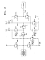
- FIG. 10 is a circuit diagram showing an exemplary Y driver circuit for generating panel driving signals shown in FIGS. 9A and 9B;
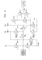
- FIG. 11 is a circuit diagram showing another exemplary Y driver circuit for generating the panel driving signals shown in FIGS. 9A and 9B.
- FIG. 5 is a view for explaining a display panel driving method, which groups scanning electrodes into a plurality of groups (n groups) and divides a frame into a plurality of sub-fields for each group to thereby drive each of the groups individually.
- each the group represents a gray-scale value by a combination of 8 sub-fields, as described with reference to FIG. 3.
- the scanning electrodes When scanning electrodes are grouped into a plurality of groups, the scanning electrodes can be divided into a predetermined number of groups according to their physical locations. For example, in a case where a panel consists of 800 scanning lines, it is possible to divide the 800 scanning lines into 8 groups, set 1-th through 100-th scanning lines to a first group, and set 101-th through 200-th scanning lines to a second group. Also, when grouping the scanning lines, it is possible to group scanning lines spaced by a predetermined interval into a group, as well as to group neighboring scanning lines into a group.
- 1-th, 9-th, 17-th, ..., (8k+1)-th scanning lines can be allocated to a first group, and 2-th, 10-th, 18-th, ..., (8k+2)-th scanning lines can be allocated to a second group. It is also possible to group the scanning lines in an irregular manner as necessary.
- FIG. 6 is a timing diagram showing sustain periods PS for explaining a display panel driving method according to an exemplary embodiment of the present invention.
- cells of a display panel are divided into two scanning electrode groups Y g1 and Y g2 .
- a sustain discharge of selected display cells is carried out by applying a high level and a low level of a sustain discharge signal alternately to scanning electrodes and a common electrode. At this time, if a potential difference formed between the scanning electrodes and the common electrode is greater than a break-down voltage, a discharge is carried out. Otherwise, no discharge is carried out.
- a sustain discharge signal of a common electrode X has a high level V S and a low level V L1 .
- a sustain discharge signal of each of the scanning electrodes Y g1 and Y g2 has a high level V S , a first low level V L1 and a second low level V L2 .
- a voltage higher than the break-down voltage is formed between the scanning electrodes Y g1 and Y g2 and the common electrode X, by a potential difference between the high level V S of the scanning electrodes Y g1 and Y g2 and the low level V L1 of the common electrode X. Also, a voltage higher than the break-down voltage is formed between the common electrode X and the scanning electrodes Y g1 and Y g2 by a potential difference between the high level V S of the common electrode X and the first low level V L1 of the scanning electrodes Y g1 and Y g2 .
- a voltage lower than the break-down voltage is formed between the common electrode X and the scanning electrodes Y g1 and Y g2 by a potential difference between the high level V S of the common electrode X and the second low level V L2 of the scanning electrodes Y g1 and Y g2 .
- a sustain discharge signal is applied in an order of V L1 -> V S -> V L2 -> V S -> V L1 -> V S -> V L1 -> V S .
- no discharge is carried out in the following sustain discharge period PS if the corresponding first scanning electrode group Y g1 is in the first low level V L1 and the corresponding common electrode X is in a high level.
- the first scanning electrode group Y g1 is changed to the high level V S and the common electrode X is changed to the low level V L2 , a discharge is carried out in the corresponding display cell.
- a sustain discharge signal is applied in an order of V L1 -> V S -> V L1 -> V S -> V L1 -> V S -> V L2 -> V S .
- no discharge is carried out in the following sustain period PS if the corresponding second scanning electrode group Y g2 is in the first low level V L1 and the corresponding common electrode X is in a high level.
- a discharge is carried out in the corresponding display cell, when the second scanning electrode group Y g2 is changed to the high level V S and the common electrode X is changed to the low level V L1 .
- the second scanning electrode group Y g2 is changed to the first low level V L1 and the common electrode X is changed to the high level V S , a discharge is carried out.
- the high level V S and the first low level V L1 are applied alternately to the second scanning electrode group Y g2 and the common electrode X, so that discharges are carried out five times.
- the second scanning electrode group Y g2 is changed to the high level V S and the common electrode X is changed to the low level V L1 , no discharge is carried out.
- discharges are carried out five times between the common electrode X and the second scanning electrode group Y g2 .
- FIG. 7 is a conceptual scheme for explaining a display panel driving method based on an address/sustain discharge mixed method, according to an exemplary embodiment of the present invention.
- the present embodiment is aimed to achieve a stable sustain discharge by minimizing a temporal gap between an address period and a sustain period in implementing gray-scale, as will be described in detail as follows.
- Scanning electrodes of a panel are grouped into a plurality of groups G1 through Gn and are addressed sequentially for each group.
- a sustain discharge pulse is applied to the scanning electrode group, thereby applying a sustain period to the corresponding electrode group.
- the sustain period can be applied selectively to different scanning electrode groups having been addressed.
- the address period can be applied to different scanning electrode groups not having been addressed.
- the numbers of the scanning electrodes belonging to each of the groups can be the same in all the groups or can be different for each of the groups.
- a sub-field includes a reset period R, an address/sustain mixed period T1, a common sustain period T2 and a brightness compensation period T3.
- dotted blocks represent address periods in the address/sustain mixed period T1
- left oblique lined blocks represent sustain periods in the address/sustain mixed period T1
- a checked block represents a sustain period in the_common sustain period T2
- right oblique lined blocks represent sustain periods in the brightness compensation period T3.
- the common sustain period T2 and the brightness compensation period T3 may be omitted according to a gray-scale value allocated to a corresponding sub-field.
- a sub-field with a relatively low gray-scale requires a relatively short sustain discharge period for implementing the gray-scale.
- a sub-field with a relatively high gray-scale requires a relatively long sustain discharge period.
- a sub-field with a relatively low gray-scale may have only a single address/sustain mixed period T1.
- a sub-field with a relatively high gray-scale may have an address/sustain mixed period T1, a common sustain period T2 and a brightness compensation period T3.
- a sub-field with a middle level of gray-scale can have an address/sustain mixed period T1 and a brightness compensation period T3 without a common sustain period T2.
- reset pulses are applied to all the scanning line groups to initialize states of wall charges of cells.
- scanning pulses are applied sequentially from a first scanning electrode line Y 11 to a final scanning electrode line Y 1m in a first group G1, so that an address period AG1 is applied to the first group G 1.
- a sustain discharge period S11 is applied to these addressed cells in order to sustain-discharge the cells using a predetermined number of sustain pulses.
- an address period AG2 is applied to cells belonging to a second group G2.
- a first sustain period S21 is applied to the second group G2.
- a second sustain period S12 is also applied to the first group G2 having been addressed.
- gray-scale is obtained in the first sustain period S11 of the first group G1
- the second sustain period S12 of the first group G1 can be omitted.
- cells still not entering the address period are maintained in a pause state.
- an address period SG3 and a first sustain period S31 are applied to a third group G3 in the same manner as described above.
- the sustain periods S13 and S22 can be applied to the cells of the first and second groups G1 and G2 having been addressed. If the desired gray-scale is obtained during the first sustain discharge periods S13 and S22 of the first and second groups, the additional sustain discharge periods S 13 and S22 can be omitted.
- the scanning pulses are applied sequentially to the scanning electrodes belonging to the final group Gn in the same manner as described above, so that an address period AGn is applied to the final group Gn.
- a sustain period Sn1 is applied to the final group Gn.
- the sustain period Sn1 is also applied to cells of different groups.
- FIG. 7 shows an example where the sustain period is applied to cells of different groups having been addressed while a sustain period is applied to cells of a certain group. If the number of the sustain pulses applied during a unit sustain period is constant and accordingly brightness created by the sustain pulses is constant, the brightness of the cells of the first group will be n times of that of the cells of the n-th group. Likewise, the brightness of the cells of the second group will be n-1 times of that of the cells of the n-th group. Also, the brightness of the cells of the (Gn-1)-th group will be two times that of the cells of the n-th group. In order to compensate for such brightness differences for each of the groups, a predetermined additional sustain period is needed. Such an additional sustain period is the brightness compensation period T3 shown in FIG. 7.
- the brightness compensation period T3 is applied selectively to each of the groups so that gray-scales of the cells of each of the groups become uniform.
- the common sustain period T2 is a period for applying sustain pulses to all the cells at the same time during a predetermined time.
- the common sustain period T2 can be applied selectively in the case where gray-scales allocated to each of sub-fields are not obtained in the address/sustain mixed period T1 or in the common sustain period T2 and the brightness compensation period T3.
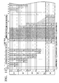
- the common sustain period T2 can follow the address/sustain mixed period T1 as shown in FIG. 12, or can follow the brightness compensation period T3.
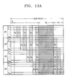
- FIG. 8A is a view for explaining a display panel driving method which drives a display panel including pixels divided into four groups on the basis of the display panel driving method of FIG 7, according to an exemplary embodiment of the present invention.
- a sub-field has a reset period R, an address/sustain mixed period T1, a common sustain period T2, and a brightness compensation period T3.
- Detailed descriptions for the sub-field have been provided above with reference to FIG. 7.
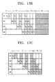
- FIG. 8B shows an example in which the brightness compensation period T3 is used prior to the common sustain period T2, as a modified example of FIG. 8A.
- the embodiments shown in FIGS. 8A and 8B may be useful in implementing sub-fields with a high weight. Also, the length of the common sustain period T2 may be changed appropriately according to the weight of a corresponding sub-field.
- FIG. 8C shows an example in which a sub-field has only an address/sustain mixed period T1 and a brightness compensation period T3 without a common sustain period T2, as a modified example of FIG. 8A.
- supplying sustain pulses is terminated to at least a group during the address/sustain mixed period T1. That is, in FIG. 8C, a sustain discharge for the first group G1 is complete in the address/sustain mixed period T1.
- the embodiment of FIG. 8C may be useful in implementing a sub-field with a middle level of weight.
- FIG. 8D shows an example in which a sub-field has only an address/sustain mixed period T1, as another modified example of FIG. 8A. After an address operation and a sustain discharge operation for a group are terminated, an address operation and a sustain discharge operation for a different group are performed sequentially. Therefore, the address/sustain mixed period T1 is applied sequentially to the first through final groups.
- the embodiment of FIG. 8D may be useful in implementing a sub-field with a low weight.
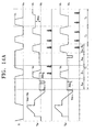
- FIG. 9A is a timing diagram of sub-field driving signals when the driving method of FIG. 8A is applied to two scanning electrode groups Y g1 and Y g2 , according to an embodiment of the present invention.
- a sub-field After a reset period R, a sub-field includes an address/sustain mixed period T1, a common sustain period T2, and a brightness compensation period T3, in this order.
- reset pulses are applied to all scanning electrode line groups so to initialize the states of wall charges of cells.
- a first address period AG1 of the first scanning electrode group Y g1 is performed and a sustain period S11 of the second scanning electrode group Y g2 is performed.
- An address period AG2 of the second scanning electrode group A g2 is performed after the sustain period S11 of the first scanning electrode group Y g1 terminates.
- a second sustain period S12 of the first scanning electrode group Y g1 is performed and, simultaneously, a first sustain period S21 of the second scanning electrode group Y g2 is performed.
- a common sustain period T2 starts.
- a discharge is carried out in all the first and second scanning electrode groups Y g1 and Y g2 .
- the brightness compensation period T3 starts.
- a discharge is carried out only between the second scanning electrode group Y g2 and the common electrode X. Comparing the potential levels of the sustain discharge signal shown in FIGS. 9A and 94B with those of the sustain discharge signal shown in FIG. 6, the high levels of both the sustain discharge signals are the same as V S ⁇ . However, the first low level of the sustain discharge signal of FIG. 11 is V L1 and the first low level of the sustain discharge signal of FIG.
- the second low level of the sustain discharge signal of FIG. 6 is V L2 and the second low level of the sustain discharge signal of FIG. 9A is ⁇ V SC .
- the second low level of the sustain discharge signal of FIG. 6 is V L2 and the second low level of the sustain discharge signal of FIG. 9B is ⁇ V SC .At this time, if a potential difference formed between the scanning electrode and the common electrode is greater than a discharge start voltage, a discharge is carried out. Otherwise, no discharge is carried out.
- the sustain discharge signal of the common electrode has a high level V S and a first low level V G .
- each of the sustain discharge signals of the scanning electrode groups Y g1 and Y g2 has a high level V S , a first low level V G and a second low level ⁇ V SC .
- the V S and V G are applied alternately between the first scanning electrode group Y g1 and the common electrode X, so that discharges are carried out twice.
- the V S and V G are applied respectively to the second scanning electrode group Y g2 and the common electrode X, so that a discharge is carried out one time.
- the V S and V G are also applied respectively to the first scanning electrode group Y g1 and the common electrode X, so that a discharge is carried out one time in the cells selected during the address period AG1 of the first group Y g1 .
- the V G and V S are applied alternately to the scanning electrode groups Y g1 and Y g2 and the common electrode X, so that discharges are carried out twice in the first and second groups Y g1 and Y g2 .
- ⁇ V SC and V S are applied sequentially to the first scanning electrode group Y g1
- the V G and V S are applied sequentially to the second scanning electrode group Y g2 . Accordingly, in the brightness compensation period T3, no discharge is carried out in the cells of the first group Y g1 and discharges are carried out twice in the cells of the second group Y g2 .
- each of the first and second groups Y g1 and Y g2 is discharged five times
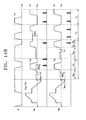
- FIG. 9B is a timing diagram of sub-field driving signals when the driving method of FIG. 8B is applied to the two scanning electrode groups Y g1 and Y g2 , according to an embodiment of the present invention.
- FIG. 9B and FIG. 9A A difference between FIG. 9B and FIG. 9A is that the common sustain period T2 and the brightness compensation period T3 are reversed when compared to each other.
- ⁇ V SC and V S are applied sequentially to the first scanning electrode groups Y g1
- V G and V S are applied sequentially to the second scanning electrode group Y g2 .
- no discharge is carried out in the cells of the first group Y g1 and discharges are carried out two times only in the cells of the second group Y g2 .
- each of the first and second groups Y g1 and Y g2 is discharged five times.
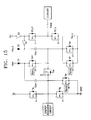
- FIG. 10 is a circuit diagram of an exemplary Y driver circuit for generating the panel driving signals shown in FIGS. 9A and 9B.
- An energy recovery circuit connected to a node located between switches Ys and Yg includes a capacitor for energy accumulation and an inductor, wherein the energy recovery circuit enhances the power efficiency using a LC resonance due to a panel capacitance of the capacitor and an inductance of the inductor.
- An example of such an energy recovery circuit is disclosed in U.S. Patents No. 4,866,349 and No. 5,670,974.
- a rising ramp interval V S through V S +V set is applied to the panel via a path passing through the switch Ys, a capacitor Cset and switches Yrrl and SC_L.
- a falling ramp interval V S through V SC_L is applied to the panel via a path passing through switches Yfr and SC_L in the state that the switches Ys and Ypp are turned on.
- a left portion is a sustain driving part
- a upper portion is a scanning signal high level applying part
- a lower portion is a scanning signal low level applying part.
- the sustain driving part includes a switch Y S connected to a high level source V S for providing a high level of a sustain signal, and a switch Yg connected to a first low level source GND for providing a low level of the sustain signal.
- the sustain driving part can further include a voltage source Vset and switches Yrr1 and Ypp in order to provide a ramp reset signal in the reset period.
- the scanning signal high level applying part includes a scanning capacitor Csc and a high level scanning source V SC_H .
- the scanning signal high level applying part is connected to a scanning electrode line of a panel through a high level scanning switch SC_ H.
- the scanning signal low level applying part includes a switch Ysc and a low level scanning source V SC_L .
- the scanning signal low level applying part is connected to the scanning electrode line of the panel through the low level scanning switch SC_ L.
- a first switch S1 is connected to a node located between the high level scanning source V SC_H and the scanning capacitor Csc.
- a second low level applying part V L2 is connected through a second switch S2 to a node located between the first switch S1 and the high level scanning switch SC_H.
- the first switch S1 and the second switch S2 are turned on so as to be toggled to each other.
- the first switch S1 and the second switch S2 control a second low level of a sustain discharge signal supplied to the panel in the brightness compensation period T3.
- the V SC_H is a different voltage source from the V L2 .
- ⁇ V SC as a second low level of a sustain discharge signal is applied.
- the first switch S1 is turned on and the second switch S2 is turned off.
- V L2 instead of ⁇ V SC , as the second low level of the sustain discharge signal, should be applied during the brightness compensation period T3 of FIG. 14A, the first switch S1 is turned off and the second switch S2 is turned on.
- a rising ramp period of V s through V s + V set is applied to the panel via a path passing through a switch Ys, a capacitor Cset and switches Yrr1 and SC_L.
- a falling ramp period of V s through V SC_L is applied to the panel via a path passing through a switch Yfr and the switch SC_L in the state that the switches Ys and Ypp are turned on.
- a final potential of the reset period PR is a scanning potential V SC-L with a low level.
- an address period AG1 of the first group Y g1 appears.
- the first switch S1 is turned on and the second switch S2 is turned off.
- a high level scanning voltage V SC_L + ⁇ Vsc is applied to the panel.
- a low level scanning voltage V SC-L is applied to the panel.
- the ⁇ V SC is a voltage applied to the scanning capacitor Csc, as a voltage difference between the high level scanning source V SC_H and the low level scanning source V SC_L .
- the switches Ys and Yg are turned on alternately, so that a sustain pulse is applied to the panel through the switches Ypp and SC_L.
- a switch for applying the V s and a switch for applying the V G are turned on alternately in the X driver so that a X driving signal is generated in the period S11. Therefore, in the sustain period S11 of the first group Y g1 , discharges are carried out two times in the cells selected in the address period AG1 of the first group Y g1 .
- the address period AG2 of the second group Y g2 is performed by the same switching mechanism as in the address period AG1 of the first group Y g1 , in the circuit of FIG. 15. Then, a sustain discharge is carried out in the second sustain period S12 of the first group Y g1 , the first sustain period S21 of the second group Y g2 , and the common sustain period T2, by the same switching mechanism as in the first sustain period S11 of the first group Y g1 .
- a brightness compensation period T3 starts.
- the first switch S1 is turned off and the second switch S2 is turned on.
- ⁇ V SC is applied as a second low level of the sustain discharge signal.
- the first switch S1 is turned on and the second switch S2 is maintained in a turned-off state.
- the switches Ys, Ypp and SC_L are turned on.
- the switches Yg, Ypp and SC_L are turned on.
- the switches Yg, Ypp and SC_H are turned on.
- V L2 instead of the ⁇ V SC , as the second low level of the sustain discharge signal to the panel in the brightness compensation period T3 of FIG. 9A, the first switch S1 is turned off, the second switch S2 is turned on and the switch SC_H is turned on.
- FIG. 11 is a circuit diagram of another exemplary Y driver circuit for generating the panel driving signals shown in FIGS. 9A and 9B.
- FIG.11 shows a circuit where switches Ysch and Ysp are added to the circuit of FIG. 10.
- the switch Ysch operates in the same manner as the first switch S1 of FIG. 10, in the brightness compensation period T3.
- a switching operation for implementing the reset period PR is the same as described above with reference to FIG.10.
- the second switch S2 is turned off. At this time, if the switches Ysch and SC_H are turned on and the low level scanning switch SC_L is turned off, a scanning voltage V SC_L + ⁇ V SC with a high level is applied to the panel. If the high level scanning switch SC_H is turned off and the low level scanning switch SC_L is turned on, the low level scanning voltage V SC_L is applied to the panel.
- the ⁇ V SC is a voltage applied to the scanning capacitor Csc, as a voltage difference between the high level voltage source V SC_H and the low level voltage source V SC_L .
- the switches Ys and Yg are turned on alternately, so that sustain pulses are applied to the panel via the switches Ypp and SC_L.
- a switch for applying the V S and a switch for applying the V G are turned on alternately in the X driver, so that a X driving signal is generated in the sustain period S11.
- the ⁇ V SC as the second low level of the sustain discharge signal, is applied in the brightness compensation period T3.
- the switch Ysch is turned on and the second switch S2 is maintained in a turned-off state.
- the switches Ys, Ypp and SC_L are turned on.
- the switches Yg, Ypp and SC_L are turned on.
- the switches Ypp, Ysch and SC_H are turned on.
- V L2 instead of ⁇ V SC , as the second low level of the sustain discharge signal to the panel in the brightness compensation period T3 of FIG. 9A, the switch Ysch is turned off, the second switch S2 is turned on and the switch SC_H is turned on.
- the first switch S1 and the second switch S2 may be omitted in the circuits of FIGS. 10 and 11. That is, it will be appreciated that the panel driving method according to the present invention may also be implemented using other conventional circuits, if the ⁇ V SC as the second low level of the sustain discharge signal is applied to the panel in the brightness compensation period T3.
- the display panel driving method according to the present invention may be used by a display apparatus which sequentially provides an address period for selecting cells to be turned on and a sustain period for lighting the selected cells.
- a display apparatus which sequentially provides an address period for selecting cells to be turned on and a sustain period for lighting the selected cells.
- the present invention can be applied to an image display device which sequentially provides an address period and a sustain period using space charges, such as an AC type PDP, a DC type PDP, an EL display device, or a liquid display device.
- the present invention may be embodied as a program stored on a computer readable medium that can be run on a general computer.
- the computer readable medium includes but is not limited to storage media such as magnetic storage media (e.g., ROM's, floppy disks, hard disks, etc.), optically readable media (e.g., CD-ROMs, DVDs, etc.).
- a program stored in the readable medium may be a series of instruction commands that are used directly or indirectly in a medium with information processing capability, such as a computer.
- the term "computer” should be interpreted to include all mediums with information processing capability, which include, but are not limited to, a memory, an input/output device, and an operation device and perform particular functions using a program.
- the logic controller 202 and the image processor 200 included in the panel driving apparatus shown in FIG. 2 are constructed into an integrated circuit including a memory and a processor therein.
- the memory may store a program for a method for driving the panel.
- the program stored in the memory is executed, so that the addressing and sustain operations according to the present invention can be performed.
- the program for executing such a panel driving method therein can be stored on a recording medium.
- the program for executing the panel driving method may be written in schematic or VHDL (Very high speed integrated circuit Hardware Description Language) and be executed by a programmable integrated circuit, for example, FPGA (Field Programmable Gate Array).
- VHDL Very high speed integrated circuit Hardware Description Language
- FPGA Field Programmable Gate Array
- the recording medium includes the programmable integrated circuit.
Landscapes
- Engineering & Computer Science (AREA)
- Physics & Mathematics (AREA)
- Power Engineering (AREA)
- Plasma & Fusion (AREA)
- Computer Hardware Design (AREA)
- General Physics & Mathematics (AREA)
- Theoretical Computer Science (AREA)
- Control Of Indicators Other Than Cathode Ray Tubes (AREA)
- Transforming Electric Information Into Light Information (AREA)
- Control Of Gas Discharge Display Tubes (AREA)
Applications Claiming Priority (2)
| Application Number | Priority Date | Filing Date | Title |
|---|---|---|---|
| KR2004021551 | 2004-03-30 | ||
| KR1020040021551A KR100509609B1 (ko) | 2004-03-30 | 2004-03-30 | 디스플레이 패널구동방법 및 장치 |
Publications (2)
| Publication Number | Publication Date |
|---|---|
| EP1585095A2 true EP1585095A2 (de) | 2005-10-12 |
| EP1585095A3 EP1585095A3 (de) | 2008-03-12 |
Family
ID=34910079
Family Applications (1)
| Application Number | Title | Priority Date | Filing Date |
|---|---|---|---|
| EP05075346A Withdrawn EP1585095A3 (de) | 2004-03-30 | 2005-02-09 | Verfahren und Einrichtung zum Steuern einer Anzeigetafel |
Country Status (5)
| Country | Link |
|---|---|
| US (1) | US20050219157A1 (de) |
| EP (1) | EP1585095A3 (de) |
| JP (1) | JP4188898B2 (de) |
| KR (1) | KR100509609B1 (de) |
| CN (1) | CN1677461A (de) |
Cited By (1)
| Publication number | Priority date | Publication date | Assignee | Title |
|---|---|---|---|---|
| EP1801771A1 (de) * | 2005-12-21 | 2007-06-27 | Samsung SDI Co., Ltd. | Vorrichtung und Verfahren zur Ansteuerung einer Anzeigetafel |
Families Citing this family (8)
| Publication number | Priority date | Publication date | Assignee | Title |
|---|---|---|---|---|
| KR100719597B1 (ko) * | 2006-02-07 | 2007-05-17 | 삼성에스디아이 주식회사 | 플라즈마 디스플레이 패널의 구동방법 |
| US7719491B2 (en) * | 2006-02-13 | 2010-05-18 | Chunghwa Picture Tubes, Ltd. | Method for driving a plasma display panel |
| KR100740094B1 (ko) | 2006-02-28 | 2007-07-16 | 삼성에스디아이 주식회사 | 플라즈마 표시 장치 및 그 구동 방법 |
| KR100786876B1 (ko) | 2006-12-27 | 2007-12-20 | 삼성에스디아이 주식회사 | 플라즈마 표시 장치 및 그 구동 방법 |
| JP4226648B2 (ja) * | 2007-01-24 | 2009-02-18 | パナソニック株式会社 | プラズマディスプレイパネル駆動回路およびプラズマディスプレイ装置 |
| KR100908719B1 (ko) * | 2007-03-13 | 2009-07-22 | 삼성에스디아이 주식회사 | 플라즈마 표시 장치 및 그 구동 장치 |
| KR100839386B1 (ko) * | 2007-03-26 | 2008-06-20 | 삼성에스디아이 주식회사 | 플라즈마 표시 장치 및 그 구동 방법 |
| CN107818760B (zh) * | 2016-09-14 | 2019-11-19 | 上海和辉光电有限公司 | 显示装置的显示方法、显示面板及显示装置 |
Citations (4)
| Publication number | Priority date | Publication date | Assignee | Title |
|---|---|---|---|---|
| US5670974A (en) | 1994-09-28 | 1997-09-23 | Nec Corporation | Energy recovery driver for a dot matrix AC plasma display panel with a parallel resonant circuit allowing power reduction |
| US5684499A (en) | 1993-11-29 | 1997-11-04 | Nec Corporation | Method of driving plasma display panel having improved operational margin |
| US6710755B1 (en) | 1999-10-12 | 2004-03-23 | Pioneer Corporation | Method for driving plasma display panel |
| EP1424677A2 (de) | 2002-11-26 | 2004-06-02 | Samsung SDI Co., Ltd. | Verfahren und Einrichtung zur Steuerung Plasmaanzeigetafel, mit gemischten Aufrechterhaltungsperioden und Adressenperioden |
Family Cites Families (7)
| Publication number | Priority date | Publication date | Assignee | Title |
|---|---|---|---|---|
| US4866349A (en) * | 1986-09-25 | 1989-09-12 | The Board Of Trustees Of The University Of Illinois | Power efficient sustain drivers and address drivers for plasma panel |
| JP3259253B2 (ja) * | 1990-11-28 | 2002-02-25 | 富士通株式会社 | フラット型表示装置の階調駆動方法及び階調駆動装置 |
| JP3499058B2 (ja) * | 1995-09-13 | 2004-02-23 | 富士通株式会社 | プラズマディスプレイの駆動方法及びプラズマディスプレイ装置 |
| US6262160B1 (en) * | 1999-02-10 | 2001-07-17 | Nippon Bee Chemical Co., Ltd | Water base adhesion promotor for polypropylene and method for coating to polypropylene materials using the promotor |
| EP1172787A1 (de) * | 2000-07-13 | 2002-01-16 | Deutsche Thomson-Brandt Gmbh | Graustufensteuerung einer Matrixanzeige |
| JP4945033B2 (ja) * | 2001-06-27 | 2012-06-06 | 日立プラズマディスプレイ株式会社 | プラズマディスプレイ装置 |
| US6903515B2 (en) * | 2002-06-21 | 2005-06-07 | Lg Electronics Inc. | Sustain driving apparatus and method for plasma display panel |
-
2004
- 2004-03-30 KR KR1020040021551A patent/KR100509609B1/ko not_active Expired - Fee Related
- 2004-09-30 JP JP2004288334A patent/JP4188898B2/ja not_active Expired - Fee Related
-
2005
- 2005-01-07 US US11/030,202 patent/US20050219157A1/en not_active Abandoned
- 2005-02-09 EP EP05075346A patent/EP1585095A3/de not_active Withdrawn
- 2005-02-21 CN CNA2005100526018A patent/CN1677461A/zh active Pending
Patent Citations (4)
| Publication number | Priority date | Publication date | Assignee | Title |
|---|---|---|---|---|
| US5684499A (en) | 1993-11-29 | 1997-11-04 | Nec Corporation | Method of driving plasma display panel having improved operational margin |
| US5670974A (en) | 1994-09-28 | 1997-09-23 | Nec Corporation | Energy recovery driver for a dot matrix AC plasma display panel with a parallel resonant circuit allowing power reduction |
| US6710755B1 (en) | 1999-10-12 | 2004-03-23 | Pioneer Corporation | Method for driving plasma display panel |
| EP1424677A2 (de) | 2002-11-26 | 2004-06-02 | Samsung SDI Co., Ltd. | Verfahren und Einrichtung zur Steuerung Plasmaanzeigetafel, mit gemischten Aufrechterhaltungsperioden und Adressenperioden |
Cited By (1)
| Publication number | Priority date | Publication date | Assignee | Title |
|---|---|---|---|---|
| EP1801771A1 (de) * | 2005-12-21 | 2007-06-27 | Samsung SDI Co., Ltd. | Vorrichtung und Verfahren zur Ansteuerung einer Anzeigetafel |
Also Published As
| Publication number | Publication date |
|---|---|
| US20050219157A1 (en) | 2005-10-06 |
| CN1677461A (zh) | 2005-10-05 |
| JP4188898B2 (ja) | 2008-12-03 |
| EP1585095A3 (de) | 2008-03-12 |
| JP2005284249A (ja) | 2005-10-13 |
| KR100509609B1 (ko) | 2005-08-22 |
Similar Documents
| Publication | Publication Date | Title |
|---|---|---|
| JP3511475B2 (ja) | 表示パネルの駆動方法及び集積回路デバイス | |
| KR100354678B1 (ko) | 플라즈마 디스플레이 패널의 구동방법 | |
| KR19980079336A (ko) | 플라즈마 디스플레이 패널과, 플라즈마 디스플레이 장치 및플라즈마 디스플레이 패널의 구동 방법 | |
| JP2002215086A (ja) | プラズマディスプレイ装置の駆動方法およびプラズマディスプレイ装置 | |
| JP2004029412A (ja) | プラズマディスプレイパネルの駆動方法 | |
| US20020140639A1 (en) | Method and device for driving AC type PDP | |
| KR100626017B1 (ko) | 플라즈마 디스플레이 패널구동방법 및 패널구동장치 | |
| EP1585095A2 (de) | Verfahren und Einrichtung zum Steuern einer Anzeigetafel | |
| KR100774875B1 (ko) | 플라즈마 디스플레이 패널의 구동방법 | |
| KR100524306B1 (ko) | 플라즈마 디스플레이 패널의 리셋 방법 및 장치 | |
| KR100680709B1 (ko) | 플라즈마 디스플레이 패널의 구동 장치 | |
| KR100544139B1 (ko) | 디스플레이 패널구동장치 | |
| KR100524311B1 (ko) | 플라즈마 디스플레이 패널의 구동방법 및 장치 | |
| KR100627416B1 (ko) | 플라즈마 표시 장치의 구동 방법 | |
| JP2002108278A (ja) | プラズマディスプレイ装置およびその駆動方法 | |
| CN100520876C (zh) | 驱动等离子显示面板的方法和设备 | |
| KR20010098111A (ko) | 어드레스 전극 구동 전력 회수 회로를 갖는 플라즈마표시패널의 구동장치 | |
| KR100747169B1 (ko) | 플라즈마 디스플레이 장치 및 플라즈마 디스플레이 장치의구동 방법 | |
| KR100740109B1 (ko) | 플라즈마 표시 장치의 구동 방법 | |
| KR100631122B1 (ko) | 플라즈마 표시장치 및 그 구동방법 | |
| KR100524304B1 (ko) | 플라즈마 디스플레이 패널의 구동 방법 및 장치 | |
| KR100667558B1 (ko) | 플라즈마 디스플레이 장치 및 그 구동 방법 | |
| KR20060016567A (ko) | 플라즈마 표시 장치 및 그에 따른 구동 방법 | |
| KR100778506B1 (ko) | 플라즈마 표시 장치 및 그 구동 방법 | |
| KR100667321B1 (ko) | 플라즈마 디스플레이 장치 및 그의 구동방법 |
Legal Events
| Date | Code | Title | Description |
|---|---|---|---|
| PUAI | Public reference made under article 153(3) epc to a published international application that has entered the european phase |
Free format text: ORIGINAL CODE: 0009012 |
|
| AK | Designated contracting states |
Kind code of ref document: A2 Designated state(s): AT BE BG CH CY CZ DE DK EE ES FI FR GB GR HU IE IS IT LI LT LU MC NL PL PT RO SE SI SK TR |
|
| AX | Request for extension of the european patent |
Extension state: AL BA HR LV MK YU |
|
| RIN1 | Information on inventor provided before grant (corrected) |
Inventor name: LEE, JOO-YULLEGAL & IP TEAM, SAMSUNG SDI CO. L |
|
| PUAL | Search report despatched |
Free format text: ORIGINAL CODE: 0009013 |
|
| AK | Designated contracting states |
Kind code of ref document: A3 Designated state(s): AT BE BG CH CY CZ DE DK EE ES FI FR GB GR HU IE IS IT LI LT LU MC NL PL PT RO SE SI SK TR |
|
| AX | Request for extension of the european patent |
Extension state: AL BA HR LV MK YU |
|
| 17P | Request for examination filed |
Effective date: 20080905 |
|
| AKX | Designation fees paid |
Designated state(s): DE FR GB IT NL |
|
| STAA | Information on the status of an ep patent application or granted ep patent |
Free format text: STATUS: THE APPLICATION HAS BEEN WITHDRAWN |
|
| 18W | Application withdrawn |
Effective date: 20091019 |