EP1585372B1 - Ballast électronique avec exitation par résonance se chargeant de la génération de tension - Google Patents
Ballast électronique avec exitation par résonance se chargeant de la génération de tension Download PDFInfo
- Publication number
- EP1585372B1 EP1585372B1 EP05004714.1A EP05004714A EP1585372B1 EP 1585372 B1 EP1585372 B1 EP 1585372B1 EP 05004714 A EP05004714 A EP 05004714A EP 1585372 B1 EP1585372 B1 EP 1585372B1
- Authority
- EP
- European Patent Office
- Prior art keywords
- frequency
- lamp
- resonant circuit
- excitation
- switching transistors
- Prior art date
- Legal status (The legal status is an assumption and is not a legal conclusion. Google has not performed a legal analysis and makes no representation as to the accuracy of the status listed.)
- Expired - Lifetime
Links
- 230000005284 excitation Effects 0.000 title claims description 44
- 239000003990 capacitor Substances 0.000 claims description 32
- 238000012546 transfer Methods 0.000 claims description 13
- 238000000034 method Methods 0.000 claims description 6
- 238000001914 filtration Methods 0.000 claims description 4
- 230000009466 transformation Effects 0.000 claims description 4
- 238000005286 illumination Methods 0.000 claims 1
- 230000001939 inductive effect Effects 0.000 claims 1
- 230000001105 regulatory effect Effects 0.000 claims 1
- 238000010586 diagram Methods 0.000 description 4
- 230000000694 effects Effects 0.000 description 4
- 238000005259 measurement Methods 0.000 description 3
- 238000013459 approach Methods 0.000 description 2
- 230000008901 benefit Effects 0.000 description 2
- 238000012937 correction Methods 0.000 description 2
- 230000008878 coupling Effects 0.000 description 2
- 238000010168 coupling process Methods 0.000 description 2
- 238000005859 coupling reaction Methods 0.000 description 2
- 238000011017 operating method Methods 0.000 description 2
- 230000008569 process Effects 0.000 description 2
- 230000004044 response Effects 0.000 description 2
- 230000007704 transition Effects 0.000 description 2
- 230000002411 adverse Effects 0.000 description 1
- 230000008859 change Effects 0.000 description 1
- 230000001419 dependent effect Effects 0.000 description 1
- 238000013461 design Methods 0.000 description 1
- 238000010891 electric arc Methods 0.000 description 1
- 230000002349 favourable effect Effects 0.000 description 1
- 238000010304 firing Methods 0.000 description 1
- 230000010355 oscillation Effects 0.000 description 1
- 230000009467 reduction Effects 0.000 description 1
- 238000004513 sizing Methods 0.000 description 1
- 239000013589 supplement Substances 0.000 description 1
- 230000002123 temporal effect Effects 0.000 description 1
- 230000005428 wave function Effects 0.000 description 1
Images
Classifications
-
- H—ELECTRICITY
- H05—ELECTRIC TECHNIQUES NOT OTHERWISE PROVIDED FOR
- H05B—ELECTRIC HEATING; ELECTRIC LIGHT SOURCES NOT OTHERWISE PROVIDED FOR; CIRCUIT ARRANGEMENTS FOR ELECTRIC LIGHT SOURCES, IN GENERAL
- H05B41/00—Circuit arrangements or apparatus for igniting or operating discharge lamps
- H05B41/14—Circuit arrangements
- H05B41/26—Circuit arrangements in which the lamp is fed by power derived from DC by means of a converter, e.g. by high-voltage DC
- H05B41/28—Circuit arrangements in which the lamp is fed by power derived from DC by means of a converter, e.g. by high-voltage DC using static converters
- H05B41/288—Circuit arrangements in which the lamp is fed by power derived from DC by means of a converter, e.g. by high-voltage DC using static converters with semiconductor devices and specially adapted for lamps without preheating electrodes, e.g. for high-intensity discharge lamps, high-pressure mercury or sodium lamps or low-pressure sodium lamps
- H05B41/2881—Load circuits; Control thereof
-
- H—ELECTRICITY
- H05—ELECTRIC TECHNIQUES NOT OTHERWISE PROVIDED FOR
- H05B—ELECTRIC HEATING; ELECTRIC LIGHT SOURCES NOT OTHERWISE PROVIDED FOR; CIRCUIT ARRANGEMENTS FOR ELECTRIC LIGHT SOURCES, IN GENERAL
- H05B41/00—Circuit arrangements or apparatus for igniting or operating discharge lamps
- H05B41/14—Circuit arrangements
- H05B41/26—Circuit arrangements in which the lamp is fed by power derived from DC by means of a converter, e.g. by high-voltage DC
- H05B41/28—Circuit arrangements in which the lamp is fed by power derived from DC by means of a converter, e.g. by high-voltage DC using static converters
- H05B41/288—Circuit arrangements in which the lamp is fed by power derived from DC by means of a converter, e.g. by high-voltage DC using static converters with semiconductor devices and specially adapted for lamps without preheating electrodes, e.g. for high-intensity discharge lamps, high-pressure mercury or sodium lamps or low-pressure sodium lamps
- H05B41/2881—Load circuits; Control thereof
- H05B41/2882—Load circuits; Control thereof the control resulting from an action on the static converter
- H05B41/2883—Load circuits; Control thereof the control resulting from an action on the static converter the controlled element being a DC/AC converter in the final stage, e.g. by harmonic mode starting
-
- H—ELECTRICITY
- H05—ELECTRIC TECHNIQUES NOT OTHERWISE PROVIDED FOR
- H05B—ELECTRIC HEATING; ELECTRIC LIGHT SOURCES NOT OTHERWISE PROVIDED FOR; CIRCUIT ARRANGEMENTS FOR ELECTRIC LIGHT SOURCES, IN GENERAL
- H05B41/00—Circuit arrangements or apparatus for igniting or operating discharge lamps
- H05B41/14—Circuit arrangements
- H05B41/36—Controlling
- H05B41/38—Controlling the intensity of light
- H05B41/382—Controlling the intensity of light during the transitional start-up phase
- H05B41/388—Controlling the intensity of light during the transitional start-up phase for a transition from glow to arc
-
- Y—GENERAL TAGGING OF NEW TECHNOLOGICAL DEVELOPMENTS; GENERAL TAGGING OF CROSS-SECTIONAL TECHNOLOGIES SPANNING OVER SEVERAL SECTIONS OF THE IPC; TECHNICAL SUBJECTS COVERED BY FORMER USPC CROSS-REFERENCE ART COLLECTIONS [XRACs] AND DIGESTS
- Y02—TECHNOLOGIES OR APPLICATIONS FOR MITIGATION OR ADAPTATION AGAINST CLIMATE CHANGE
- Y02B—CLIMATE CHANGE MITIGATION TECHNOLOGIES RELATED TO BUILDINGS, e.g. HOUSING, HOUSE APPLIANCES OR RELATED END-USER APPLICATIONS
- Y02B20/00—Energy efficient lighting technologies, e.g. halogen lamps or gas discharge lamps
Definitions
- This invention relates to electronic ballasts and methods of operating high pressure discharge lamps.
- WO 2004/064457 describes a half-bridge circuit with two half-bridge switches, which is suitable for operating a high-pressure discharge lamp.
- the circuit includes an LC resonant circuit, which is excited by a third switch.
- an ignition voltage at a considerable height must be provided, for example in a range of 1.5 kV to 5 kV (single amplitude).
- the ignited lamp needs for a certain transitional period a so-called. Takeover voltage, which is increased compared to the necessary voltage of the continuous operation power supply.
- the invention is based on the technical problem of providing an electronic ballast for operating a high-pressure discharge lamp and a corresponding operating method in which the transfer voltage can be generated and controlled in a favorable manner.
- the invention relates to an electronic ballast for operating a high-pressure discharge lamp with a converter comprising a half-bridge with two switching transistors for generating a supply power for continuous operation of the lamp by a switching operation of the switching transistors and with a filter capacitor for filtering rippling interference in the power supply for the lamp the filter capacitor is part of a resonant circuit.
- the ballast is designed to excite a resonance of the resonant circuit by high-frequency operation of the switching transistors of the converter so as to produce an over-voltage compared to the steady-state supply power for the lamp during an adjoining to an ignition acquisition phase.
- a control of the amplitude of the resonance excitation is carried out according to the invention also characterized in that - similar to the buck converter operation during lamp end operation - during a conductive switching phase of the switching transistors by repeated switching off ("chopping") with a respect to the resonant frequency significantly increased frequency quasi an average amplitude reduction is achieved. Additionally or alternatively, the time duration of the switch-on of the switching transistors can be limited in total and turn out to be significantly less than half a time proportion.
- the invention relates to a corresponding lighting device with such a ballast and a suitable high-pressure discharge lamp and finally to a corresponding operating method for operating a high-pressure discharge lamp.
- the basic idea of the invention is to generate the transfer voltage by means of a resonance excitation and to use the filter capacitor as the capacitive element of a resonant circuit, which is anyway is provided for filtering the Ripplestromanomanteile.
- the excitation of the resonant circuit should be done by the same converter, with which the continuous operation of the lamp is accomplished. So it should be exploited as possible already existing components of the circuit.
- the switching operation of the switching transistors which are also used for continuous operation, to be used for resonance excitation.
- the resonance excitation takes place with an excitation fundamental frequency of the switching operation of the switching transistors (S 1 , S 2 ).
- the turn-on of the respective conductive switching transistor is interrupted with a modulation frequency that is above the frequency for resonance excitation, which can be described by "chopping" or modulation.
- the invention thus offers the advantage of producing and controlling the required increased transfer voltages with little effort, without the so-called DC link voltage with which the converter i. d. R. is to be increased significantly.
- an inductor element of the resonance circuit used for other reasons anyway lamp inductor or Tiefsetzerdrossel is used.
- Such a choke is necessary on the one hand because of the in many cases partially negative differential impedance of high-pressure discharge lamps and / or on the other hand because of the below-described buck converter function.
- no further elements are provided in the resonant circuit as actually involved in the resonance elements, of course, the filter capacitor and the lamp inductor can be multi-part, as mentioned earlier for the filter capacitor.
- the half-bridge according to the invention can be operated in continuous operation of the lamp so that it on the one hand as a low-frequency inverter for the already described at the outset "symmetrization" of the lamp operation by Sign reversal works.
- the lamp operation can also be done with a reduced voltage compared to the intermediate circuit voltage, to which the half-bridge with the respective conductive switching transistor within a half-cycle of the inverter operation similar to a buck converter reduces the DC link voltage.
- This buck converter operation of the switching transistors of the half-bridge can be integrated into a lamp current control.
- the resonant excitation characteristic of the invention is preferably at a frequency below the resonant frequency of the resonant circuit.
- the use of resonance peaks in electronic ballasts for lamps approaches resonance frequencies coming from above. In the present case, this should be reversed.
- the lamp choke or another resonance choke should not be unnecessarily large for cost and space reasons. If, due to the recharging processes during the resonant excitation, saturation of the choke occurs, its inductance would change and the resonant circuit would automatically increase its resonant frequency. This would lead to an unstable state and to a considerable component load when approaching higher frequencies. In order to control such unstable conditions, relatively fast regulators and relatively fast voltage or current measurements are necessary. The invention circumvents this problem by approaching low frequencies.
- the fundamental frequency of resonance excitation is meant. Since the excitation is usually not done with pure sine functions but with more or less rectangular shaped functions, of course Fourier shares occur at frequencies above the resonant frequency. However, these have correspondingly lower amplitudes.
- a preferred value for the excitation frequency should preferably not be above 0.9 times the resonance frequency.
- the excitation frequency is not less than 0.4 times the resonant frequency, although in many cases no excessive resonance peak is necessary to produce a sufficient transfer voltage. This is because the square wave functions have a strong harmonic at three times the fundamental frequency, which approach the resonant frequency at fundamental frequencies below 0.4 times the resonant frequency. Convenient values are between 0.4 and 0.6 times the resonant frequency. However, within the scope of this invention, it is also quite possible to work with relatively low excitation frequencies which are significantly below the 0.4-fold resonance frequency.
- the filter capacitor should have a certain minimum capacity in favor of a good filter effect. Preference is given to values of more than 1 nF / watt lamp power, in particular of more than 1.2 or 1.3 nF / watt. Of course, with multiple capacitors this applies to the total effective capacity.
- the occurring voltage increases should preferably lead to amplitudes in the range of up to 800 V (single amplitude).
- to generate the ignition voltage by resonance peaking leads to significantly larger currents and to a much greater proximity to the resonant frequency. This results in adverse effects on the allowable capacitance of the filter capacitor, which serves as a resonant capacitor, and / or for the design of the throttle.
- the ignition voltage itself is preferably generated by its own ignition circuit. This may in particular be a per se known ignition circuit with a firing capacitor whose discharge, possibly after high transformation, leads to the ignition.
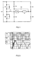
- FIG. 1 shows a known per se half-bridge topology with two switching transistors S 1 and S 2 . These are connected in series between two supply branches, between which an intermediate circuit voltage U 1 is present.
- the intermediate circuit voltage U 1 can be generated by rectifying a mains voltage with appropriate filtering and possibly power factor correction.
- the coupling capacitors C 4 and C 5 ensure that the right terminal of the lamp Lp has a potential in the middle between the potentials of the supply branches. Thus, the circuit is thus able to generate half the DC link voltage across the lamp Lp.
- Parallel to the lamp Lp is a filter capacitor C 3rd
- a tap between the lamp inductor L 1 and the ignition circuit G 1 is connected via two filter capacitors C 1 and C 2 respectively to the supply branches.
- a burning voltage of the order of magnitude of 80 V-150 V is necessary, which is actually smaller than the commonly available halved intermediate circuit voltages. Therefore, during a switching phase, in which, for example, the half-bridge transistor S 1 is conducting, it is interrupted in a clocked manner, in order to produce, together with the inductor L 1 during this switching phase To generate buck converter operation. As a result, a desired lamp burn voltage can be set by the step-down operation.
- a high-pressure discharge lamp requires a certain period of time for the transition from a glow discharge following the actual ignition to the arc discharge, in which a takeover voltage which is significantly higher than the burning voltage must be available in the range of typically 260 V-330 V. This value is regularly above the halved DC link voltage.
- the half-bridge combined with the buck converter can not easily generate this voltage.
- a resonance of a lamp resonant circuit is excited during the acquisition phase, which consists of the capacitors C 1 - C 3 and the inductor L 1 .
- This causes a voltage increase, with which the desired transfer voltage can be generated.
- this resonant excitation is used only for the transfer voltage and not for the ignition voltage, so that the filter capacitors a desired size of typically 50 nF in a ballast for a 35 W lamp or 100 nF in a ballast for a 70 W lamp and corresponding Capacities at other lamp power can have. This is in fact the effective total capacity of the capacitors C 1 to C 3 .
- Said resonant excitation for generating the transfer voltage is carried out according to the invention at lower frequencies than the resonant frequency of the lamp resonant circuit, in this embodiment, approximately at the halved resonant frequency, namely at 0.55 times the resonant frequency.
- a fast controller and a fast voltage or current measurement on the lamp resonant circuit can thus be avoided.
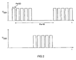
- FIG. 2 schematically shows the timing of the switching operation of the two transistors S 1 and S 2 FIG. 1 ,
- the upper part stands for the upper transistor S 1 (UGS1)
- the lower part stands for the lower transistor S 2 (UGS2).
- two periods occur here, namely a longer period between the pulse packets (PerHB) and, secondly, a shorter period within the pulse packets (PerSD).
- PerHB pulse packets
- PerSD pulse packets
- this corresponds to the already described combination of down-converter operation and half-bridge function, wherein the short period stands for the step-down operation and the longer one for the half-bridge function.
- FIG. 3 shows a real diagram of the ballast circuit FIG. 1 ,
- the uppermost curve at channel 1 shows the gate voltage of the lower half-bridge transistor S 2 , the middle curve at channel 2 the potential of the half-bridge midpoint and the lower curve at channel 3 the voltage across the lamp.
- the clear deflection of the lamp voltage approximately at the end of the first box from the left shows the ignition of the lamp with the aid of the ignition circuit G 1 .
- the thus excited high-frequency resonance is for the invention of no further concern and has to do with leakage inductances of the ignition circuit G 1 in connection with certain capacities.
- FIG. 2 illustrated "chopped" rectangular switching operation of the half-bridge transistor is already present before the ignition. Although it causes no ignition and therefore no acquisition, it does not hurt either. There does not even have to be synchronization to the ignition process. Rather, the described "chopped" half-bridge operation ensures a resonant (0.55-fold resonant frequency) excitation with a corresponding voltage overshoot across the lamp.
- FIG. 3 shows, voltage amplitudes across the lamp of almost ⁇ 400 V.
- This excitation takes place with the AC voltage shown at channel 2 at the bridge center.
- Typical resonance frequencies are approximately at 20 kHz - 40 kHz.
- the total effective capacitance of the filter capacitors is 100 nF and the inductance of the inductor L 1 is 500 ⁇ H.
- the basic excitation frequency is 12.5 kHz, the resonance frequency about 22.5 kHz.
- the amount of the takeover voltage can therefore be adjusted by the choice of the excitation frequency, on the one hand, and by the "chopper operation" on the other hand, and of course by the temporal extension of the conducting phases of the switching transistors.
- FIG. 3 shows that the "chopper frequency" is about 8 times the basic excitation frequency.
- a duty cycle within the modulation frequency ie a ratio between the switch-on phase and the associated switch-off phase by the "chopping", of about 85% is reached (the Dutycicle is only related to the modulation and not to the basic cycle).
Landscapes
- Engineering & Computer Science (AREA)
- Power Engineering (AREA)
- Circuit Arrangements For Discharge Lamps (AREA)
Claims (11)
- Ballast électronique pour faire fonctionner une lampe à décharge haute pression (Lp), comprenant- un transformateur comportant un demi-pont avec deux transistors de commutation (S1, S2) pour produire une tension de décharge pour le fonctionnement continu de la lampe (Lp) grâce à un mode de commutation des transistors de commutation (S1, S2),- un circuit résonant (L1, C1-3),- un circuit d'allumage (G1) comprenant un condensateur d'allumage pour allumer la lampe à décharge haute pression grâce à une décharge et éventuellement une augmentation de la charge du condensateur d'allumage,- le ballast électronique étant conçu pour exciter une résonance du circuit résonant (L1, C1-3) grâce à un fonctionnement à haute fréquence des transistors de commutation (S1, S2) du transformateur, afin de produire ainsi une amplitude de tension excessive par rapport à la tension de décharge pour la lampe (Lp) pendant une phase de prise en charge qui suit un allumage,- l'excitation de la résonance du circuit résonant (L1, C1-3) ayant lieu à une fréquence fondamentale d'excitation du mode de commutation des transistors de commutation (S1, S2),caractérisé en ce que- la fréquence fondamentale d'excitation du mode de commutation des transistors de commutation (S1, S2) est inférieure à une fréquence de résonance du circuit résonant, et- le ballast électronique est conçu pour abaisser l'amplitude de tension moyenne pendant la phase de prise en charge grâce à un arrêt répété durant les phases de mise en marche des transistors de commutation (S1, S2) à une fréquence nettement augmentée par rapport à la fréquence fondamentale d'excitation, et- le circuit résonant comporte un condensateur de filtrage (C1-3) pour éliminer les interférences dues aux ondulations dans la tension de décharge.
- Ballast électronique selon la revendication 1, dans lequel le circuit résonant (L1, C1-3) comporte un self de lampe (L1) en tant qu'élément inductif.
- Ballast électronique selon la revendication 1 ou 2, dans lequel le transformateur est conçu pour fonctionner en tant qu'inverseur basse fréquence en fonctionnement continu de la lampe (Lp) et en tant que convertisseur abaisseur à l'intérieur des phases de commutation de l'inverseur.
- Ballast électronique selon l'une des revendications précédentes, dans lequel l'excitation de résonance a lieu à une fréquence fondamentale ne dépassant pas 0,9 fois la fréquence de résonance du circuit résonant (L1, C1-3).
- Ballast électronique selon la revendication 4, dans lequel l'excitation de résonance a lieu à une fréquence fondamentale comprise entre 0,4 fois et 0,9 fois la fréquence de résonance du circuit résonant (L1, C1-3).
- Ballast électronique selon la revendication 1, dans lequel la fréquence de l'arrêt répété durant les phases de mise en marche des transistors de commutation (S1, S2) est nettement supérieure à la fréquence de résonance du circuit résonant (L1, C1-3).
- Ballast électronique selon l'une des revendications précédentes, dans lequel la capacité du condensateur de filtrage (C1-3) est au moins égale à 1 nF par watt de puissance de lampe.
- Ballast électronique selon l'une des revendications précédentes, dans lequel les amplitudes de tension durant l'excitation de résonance ne dépassent pas 800 V crête à crête.
- Appareil d'éclairage comprenant un ballast électronique selon l'une des revendications 1 à 8 et une lampe à décharge haute pression (L).
- Procédé pour faire fonctionner une lampe à décharge haute pression (Lp) comprenant les étapes :- allumage de la lampe à décharge haute pression au moyen d'un circuit d'allumage (G1) comportant un condensateur d'allumage grâce à une décharge et éventuellement une augmentation de la charge du condensateur d'allumage,- alimentation de la lampe en fonctionnement continu avec une tension de décharge grâce à un mode de commutation de deux transistors de commutation (S1, S2) d'un transformateur en demi-pont,- pendant une phase de prise en charge qui suit l'allumage, production d'une amplitude de tension excessive par rapport à la tension de décharge grâce à une excitation de résonance dans un circuit résonant (L1, C1-3), l'excitation de résonance ayant lieu grâce à un fonctionnement à haute fréquence des transistors de commutation (S1, S2) du transformateur en demi-pont,caractérisé en ce que- l'excitation de résonance a lieu grâce à une fréquence fondamentale d'excitation du mode de commutation des transistors de commutation (S1, S2) dont la fréquence est inférieure à la fréquence de résonance du circuit résonant,- l'amplitude de tension moyenne est abaissée pendant la phase de prise en charge grâce à un arrêt répété durant les phases de mise en marche des transistors de commutation (S1, S2) à une fréquence nettement augmentée par rapport à la fréquence fondamentale d'excitation, et- les interférences dues aux ondulations dans la tension de décharge de la lampe sont éliminées par un condensateur de filtrage (C1-3) compris dans le circuit résonant.
- Procédé pour faire fonctionner une lampe (Lp) selon la revendication 10 comprenant un ballast selon l'une des revendications 2 à 8.
Applications Claiming Priority (2)
| Application Number | Priority Date | Filing Date | Title |
|---|---|---|---|
| DE102004017479 | 2004-04-08 | ||
| DE102004017479A DE102004017479A1 (de) | 2004-04-08 | 2004-04-08 | EVG mit Resonanzanregung zur Übernahmespannungserzeugung |
Publications (2)
| Publication Number | Publication Date |
|---|---|
| EP1585372A1 EP1585372A1 (fr) | 2005-10-12 |
| EP1585372B1 true EP1585372B1 (fr) | 2013-07-10 |
Family
ID=34895538
Family Applications (1)
| Application Number | Title | Priority Date | Filing Date |
|---|---|---|---|
| EP05004714.1A Expired - Lifetime EP1585372B1 (fr) | 2004-04-08 | 2005-03-03 | Ballast électronique avec exitation par résonance se chargeant de la génération de tension |
Country Status (5)
| Country | Link |
|---|---|
| US (1) | US7145293B2 (fr) |
| EP (1) | EP1585372B1 (fr) |
| CN (1) | CN1681368A (fr) |
| CA (1) | CA2503635A1 (fr) |
| DE (1) | DE102004017479A1 (fr) |
Families Citing this family (7)
| Publication number | Priority date | Publication date | Assignee | Title |
|---|---|---|---|---|
| US7432663B2 (en) * | 2006-09-25 | 2008-10-07 | Osram Sylvania Inc. | Circuit for igniting a high intensity discharge lamp |
| US7432664B2 (en) * | 2006-09-29 | 2008-10-07 | Osram Sylvania Inc. | Circuit for powering a high intensity discharge lamp |
| KR101073302B1 (ko) * | 2007-01-10 | 2011-10-12 | 오스람 아게 | 고압 방전 램프를 동작시키기 위한 회로 어레인지먼트 및 방법 |
| WO2008128577A1 (fr) * | 2007-04-24 | 2008-10-30 | Osram Gesellschaft mit beschränkter Haftung | Circuiterie pour l'allumage et l'utilisation d'une lampe à décharge |
| KR20100005241A (ko) * | 2007-05-07 | 2010-01-14 | 오스람 게젤샤프트 미트 베쉬랭크터 하프퉁 | 고압 방전 램프들을 점화시키고 시동시키기 위한 방법 |
| DE102011089553A1 (de) * | 2011-12-22 | 2013-06-27 | Robert Bosch Gmbh | Elektronisches Vorschaltgerät für eine Gasentladungslampe |
| ITGE20120058A1 (it) * | 2012-06-20 | 2013-12-21 | Umpi R & D S R L | Sistema d'alimentazione per un impianto d'illuminazione pubblica dotato di servizi ausiliari integrati |
Citations (3)
| Publication number | Priority date | Publication date | Assignee | Title |
|---|---|---|---|---|
| US5696798A (en) * | 1993-09-30 | 1997-12-09 | Rockwell Semiconductor Systems, Inc. | Multiple antenna home base for digital cordless telephones |
| DE19644115A1 (de) * | 1996-10-23 | 1998-04-30 | Patent Treuhand Ges Fuer Elektrische Gluehlampen Mbh | Schaltungsanordnung zum Betrieb einer Hochdruckentladungslampe sowie Beleuchtungssystem mit einer Hochdruckentladungslampe und einem Betriebsgerät für die Hochdruckentladungslampe |
| US20020047609A1 (en) * | 1997-12-12 | 2002-04-25 | Matsushita Electric Works R&D Laboratory | Ballast for discharge lamp |
Family Cites Families (12)
| Publication number | Priority date | Publication date | Assignee | Title |
|---|---|---|---|---|
| CA2104252A1 (fr) * | 1992-08-20 | 1994-02-21 | Charles B. Mattas | Circuit de ballast |
| US5426350A (en) * | 1993-11-18 | 1995-06-20 | Electric Power Research Institute, Inc. | High frequency transformerless electronics ballast using double inductor-capacitor resonant power conversion for gas discharge lamps |
| DE19508468B4 (de) * | 1994-11-25 | 2006-05-24 | Matsushita Electric Works, Ltd., Kadoma | Stromversorgungseinrichtung |
| US5623187A (en) * | 1994-12-28 | 1997-04-22 | Philips Electronics North America Corporation | Controller for a gas discharge lamp with variable inverter frequency and with lamp power and bus voltage control |
| US5932976A (en) * | 1997-01-14 | 1999-08-03 | Matsushita Electric Works R&D Laboratory, Inc. | Discharge lamp driving |
| DK1042942T3 (da) * | 1997-07-24 | 2002-12-02 | Noontek Ltd | Elektronisk ballast til en gasudladningslampe |
| US6459215B1 (en) * | 2000-08-11 | 2002-10-01 | General Electric Company | Integral lamp |
| US6459214B1 (en) * | 2001-04-10 | 2002-10-01 | General Electric Company | High frequency/high power factor inverter circuit with combination cathode heating |
| DE10210629A1 (de) * | 2002-03-11 | 2003-09-25 | Knobel Lichttech | Zündschaltung für eine Hochdruckentladungslampe |
| DE10235217A1 (de) * | 2002-08-01 | 2004-02-19 | Patent-Treuhand-Gesellschaft für elektrische Glühlampen mbH | Schaltungsvorrichtung und Verfahren zum Betreiben einer Lampe |
| WO2004064457A1 (fr) * | 2003-01-14 | 2004-07-29 | Koninklijke Philips Electronics N.V. | Circuit |
| US7075251B2 (en) * | 2003-12-05 | 2006-07-11 | General Electric Company | Universal platform for phase dimming discharge lighting ballast and lamp |
-
2004
- 2004-04-08 DE DE102004017479A patent/DE102004017479A1/de not_active Withdrawn
-
2005
- 2005-03-03 EP EP05004714.1A patent/EP1585372B1/fr not_active Expired - Lifetime
- 2005-04-06 CA CA002503635A patent/CA2503635A1/fr not_active Abandoned
- 2005-04-08 CN CNA2005100648852A patent/CN1681368A/zh active Pending
- 2005-04-08 US US11/101,390 patent/US7145293B2/en not_active Expired - Lifetime
Patent Citations (3)
| Publication number | Priority date | Publication date | Assignee | Title |
|---|---|---|---|---|
| US5696798A (en) * | 1993-09-30 | 1997-12-09 | Rockwell Semiconductor Systems, Inc. | Multiple antenna home base for digital cordless telephones |
| DE19644115A1 (de) * | 1996-10-23 | 1998-04-30 | Patent Treuhand Ges Fuer Elektrische Gluehlampen Mbh | Schaltungsanordnung zum Betrieb einer Hochdruckentladungslampe sowie Beleuchtungssystem mit einer Hochdruckentladungslampe und einem Betriebsgerät für die Hochdruckentladungslampe |
| US20020047609A1 (en) * | 1997-12-12 | 2002-04-25 | Matsushita Electric Works R&D Laboratory | Ballast for discharge lamp |
Also Published As
| Publication number | Publication date |
|---|---|
| CN1681368A (zh) | 2005-10-12 |
| CA2503635A1 (fr) | 2005-10-08 |
| EP1585372A1 (fr) | 2005-10-12 |
| US20050225260A1 (en) | 2005-10-13 |
| DE102004017479A1 (de) | 2005-10-27 |
| US7145293B2 (en) | 2006-12-05 |
Similar Documents
| Publication | Publication Date | Title |
|---|---|---|
| DE60024215T2 (de) | Modulares hochfrequenz-vorschaltgerät | |
| EP0244644B1 (fr) | Disposition de circuit pour lampes à décharge basse pression travaillant en haute fréquence | |
| DE69117008T2 (de) | Wechselrichteranordnung | |
| DE4420182B4 (de) | Stromversorgungsvorrichtung | |
| EP0669789B1 (fr) | Circuit pour alimenter au moins une lampe à décharge basse-pression | |
| EP0356818B1 (fr) | Circuit alimentant une charge | |
| DE10025610A1 (de) | Ansteuergerät für eine Entladungslampe | |
| DE20221985U1 (de) | Elektronisches Vorschaltgerät für Gasentladungslampe | |
| DE102005007346A1 (de) | Schaltungsanordnung und Verfahren zum Betreiben von Gasentladungslampen | |
| EP1465330A2 (fr) | Procédé pour varier la consommation de puissance de charges capacitives | |
| EP2140731A2 (fr) | Circuiterie pour l'allumage et l'utilisation d'une lampe à décharge | |
| DE3711814C2 (de) | Elektronisches Vorschaltgerät zum Betrieb von Leuchtstofflampen | |
| EP2399429A1 (fr) | Appareil électronique de fonctionnement pour une lampe à décharge dans un gaz | |
| EP1585372B1 (fr) | Ballast électronique avec exitation par résonance se chargeant de la génération de tension | |
| DE102008052701A1 (de) | Zündvorrichtung und Beleuchtungsgerät | |
| EP2417837B1 (fr) | Circuiterie et procédé de fonctionnement d'une lampe à décharge à haute pression | |
| DE10206175A1 (de) | Entladungslampen-Zündschaltung | |
| DE29622825U1 (de) | Bestrahlungsgerät | |
| EP1696713B1 (fr) | Ballast électronique avec dispositif de mesure de courant pour lampe à décharge haute-pression | |
| EP0697803A2 (fr) | Circuit pour alimenter des lampes à décharge | |
| EP1583403B1 (fr) | Ballast pour au moins une lampe | |
| EP2263423B1 (fr) | Circuit pour allumer une lampe à décharge gazeuse hid | |
| EP0671868B1 (fr) | Circuit pour l'opération en mode pulsé d'une lampe à décharge | |
| DE69924058T2 (de) | Elektronisches Vorschaltgerät , insbesondere für Hochdruck-Lampen und Neon-Röhren | |
| EP1741319A1 (fr) | Dispositif pour produire un train d'impulsions de tension electrique, notamment pour faire fonctionner des lampes a decharge capacitive |
Legal Events
| Date | Code | Title | Description |
|---|---|---|---|
| PUAI | Public reference made under article 153(3) epc to a published international application that has entered the european phase |
Free format text: ORIGINAL CODE: 0009012 |
|
| AK | Designated contracting states |
Kind code of ref document: A1 Designated state(s): AT BE BG CH CY CZ DE DK EE ES FI FR GB GR HU IE IS IT LI LT LU MC NL PL PT RO SE SI SK TR |
|
| AX | Request for extension of the european patent |
Extension state: AL BA HR LV MK YU |
|
| 17P | Request for examination filed |
Effective date: 20051107 |
|
| AKX | Designation fees paid |
Designated state(s): AT BE BG CH CY CZ DE DK EE ES FI FR GB GR HU IE IS IT LI LT LU MC NL PL PT RO SE SI SK TR |
|
| 17Q | First examination report despatched |
Effective date: 20051208 |
|
| GRAP | Despatch of communication of intention to grant a patent |
Free format text: ORIGINAL CODE: EPIDOSNIGR1 |
|
| RAP1 | Party data changed (applicant data changed or rights of an application transferred) |
Owner name: OSRAM GMBH |
|
| RIC1 | Information provided on ipc code assigned before grant |
Ipc: H05B 41/288 20060101AFI20130305BHEP Ipc: H05B 41/38 20060101ALI20130305BHEP |
|
| RAP1 | Party data changed (applicant data changed or rights of an application transferred) |
Owner name: OSRAM GMBH |
|
| GRAS | Grant fee paid |
Free format text: ORIGINAL CODE: EPIDOSNIGR3 |
|
| GRAA | (expected) grant |
Free format text: ORIGINAL CODE: 0009210 |
|
| AK | Designated contracting states |
Kind code of ref document: B1 Designated state(s): AT BE BG CH CY CZ DE DK EE ES FI FR GB GR HU IE IS IT LI LT LU MC NL PL PT RO SE SI SK TR |
|
| REG | Reference to a national code |
Ref country code: GB Ref legal event code: FG4D Free format text: NOT ENGLISH |
|
| REG | Reference to a national code |
Ref country code: CH Ref legal event code: EP Ref country code: AT Ref legal event code: REF Ref document number: 621571 Country of ref document: AT Kind code of ref document: T Effective date: 20130715 |
|
| REG | Reference to a national code |
Ref country code: IE Ref legal event code: FG4D Free format text: LANGUAGE OF EP DOCUMENT: GERMAN |
|
| REG | Reference to a national code |
Ref country code: DE Ref legal event code: R096 Ref document number: 502005013824 Country of ref document: DE Effective date: 20130905 |
|
| PG25 | Lapsed in a contracting state [announced via postgrant information from national office to epo] |
Ref country code: SI Free format text: LAPSE BECAUSE OF FAILURE TO SUBMIT A TRANSLATION OF THE DESCRIPTION OR TO PAY THE FEE WITHIN THE PRESCRIBED TIME-LIMIT Effective date: 20130710 |
|
| REG | Reference to a national code |
Ref country code: NL Ref legal event code: VDEP Effective date: 20130710 |
|
| REG | Reference to a national code |
Ref country code: LT Ref legal event code: MG4D |
|
| PG25 | Lapsed in a contracting state [announced via postgrant information from national office to epo] |
Ref country code: SE Free format text: LAPSE BECAUSE OF FAILURE TO SUBMIT A TRANSLATION OF THE DESCRIPTION OR TO PAY THE FEE WITHIN THE PRESCRIBED TIME-LIMIT Effective date: 20130710 Ref country code: IS Free format text: LAPSE BECAUSE OF FAILURE TO SUBMIT A TRANSLATION OF THE DESCRIPTION OR TO PAY THE FEE WITHIN THE PRESCRIBED TIME-LIMIT Effective date: 20131110 Ref country code: LT Free format text: LAPSE BECAUSE OF FAILURE TO SUBMIT A TRANSLATION OF THE DESCRIPTION OR TO PAY THE FEE WITHIN THE PRESCRIBED TIME-LIMIT Effective date: 20130710 Ref country code: CY Free format text: LAPSE BECAUSE OF FAILURE TO SUBMIT A TRANSLATION OF THE DESCRIPTION OR TO PAY THE FEE WITHIN THE PRESCRIBED TIME-LIMIT Effective date: 20130619 Ref country code: PT Free format text: LAPSE BECAUSE OF FAILURE TO SUBMIT A TRANSLATION OF THE DESCRIPTION OR TO PAY THE FEE WITHIN THE PRESCRIBED TIME-LIMIT Effective date: 20131111 |
|
| PG25 | Lapsed in a contracting state [announced via postgrant information from national office to epo] |
Ref country code: PL Free format text: LAPSE BECAUSE OF FAILURE TO SUBMIT A TRANSLATION OF THE DESCRIPTION OR TO PAY THE FEE WITHIN THE PRESCRIBED TIME-LIMIT Effective date: 20130710 Ref country code: FI Free format text: LAPSE BECAUSE OF FAILURE TO SUBMIT A TRANSLATION OF THE DESCRIPTION OR TO PAY THE FEE WITHIN THE PRESCRIBED TIME-LIMIT Effective date: 20130710 Ref country code: NL Free format text: LAPSE BECAUSE OF FAILURE TO SUBMIT A TRANSLATION OF THE DESCRIPTION OR TO PAY THE FEE WITHIN THE PRESCRIBED TIME-LIMIT Effective date: 20130710 Ref country code: ES Free format text: LAPSE BECAUSE OF FAILURE TO SUBMIT A TRANSLATION OF THE DESCRIPTION OR TO PAY THE FEE WITHIN THE PRESCRIBED TIME-LIMIT Effective date: 20131021 Ref country code: GR Free format text: LAPSE BECAUSE OF FAILURE TO SUBMIT A TRANSLATION OF THE DESCRIPTION OR TO PAY THE FEE WITHIN THE PRESCRIBED TIME-LIMIT Effective date: 20131011 |
|
| PG25 | Lapsed in a contracting state [announced via postgrant information from national office to epo] |
Ref country code: CY Free format text: LAPSE BECAUSE OF FAILURE TO SUBMIT A TRANSLATION OF THE DESCRIPTION OR TO PAY THE FEE WITHIN THE PRESCRIBED TIME-LIMIT Effective date: 20130710 |
|
| PG25 | Lapsed in a contracting state [announced via postgrant information from national office to epo] |
Ref country code: EE Free format text: LAPSE BECAUSE OF FAILURE TO SUBMIT A TRANSLATION OF THE DESCRIPTION OR TO PAY THE FEE WITHIN THE PRESCRIBED TIME-LIMIT Effective date: 20130710 Ref country code: CZ Free format text: LAPSE BECAUSE OF FAILURE TO SUBMIT A TRANSLATION OF THE DESCRIPTION OR TO PAY THE FEE WITHIN THE PRESCRIBED TIME-LIMIT Effective date: 20130710 Ref country code: SK Free format text: LAPSE BECAUSE OF FAILURE TO SUBMIT A TRANSLATION OF THE DESCRIPTION OR TO PAY THE FEE WITHIN THE PRESCRIBED TIME-LIMIT Effective date: 20130710 Ref country code: RO Free format text: LAPSE BECAUSE OF FAILURE TO SUBMIT A TRANSLATION OF THE DESCRIPTION OR TO PAY THE FEE WITHIN THE PRESCRIBED TIME-LIMIT Effective date: 20130710 Ref country code: DK Free format text: LAPSE BECAUSE OF FAILURE TO SUBMIT A TRANSLATION OF THE DESCRIPTION OR TO PAY THE FEE WITHIN THE PRESCRIBED TIME-LIMIT Effective date: 20130710 |
|
| PLBE | No opposition filed within time limit |
Free format text: ORIGINAL CODE: 0009261 |
|
| STAA | Information on the status of an ep patent application or granted ep patent |
Free format text: STATUS: NO OPPOSITION FILED WITHIN TIME LIMIT |
|
| PG25 | Lapsed in a contracting state [announced via postgrant information from national office to epo] |
Ref country code: IT Free format text: LAPSE BECAUSE OF FAILURE TO SUBMIT A TRANSLATION OF THE DESCRIPTION OR TO PAY THE FEE WITHIN THE PRESCRIBED TIME-LIMIT Effective date: 20130710 |
|
| 26N | No opposition filed |
Effective date: 20140411 |
|
| REG | Reference to a national code |
Ref country code: DE Ref legal event code: R097 Ref document number: 502005013824 Country of ref document: DE Effective date: 20140411 |
|
| PG25 | Lapsed in a contracting state [announced via postgrant information from national office to epo] |
Ref country code: LU Free format text: LAPSE BECAUSE OF FAILURE TO SUBMIT A TRANSLATION OF THE DESCRIPTION OR TO PAY THE FEE WITHIN THE PRESCRIBED TIME-LIMIT Effective date: 20140303 |
|
| REG | Reference to a national code |
Ref country code: CH Ref legal event code: PL |
|
| REG | Reference to a national code |
Ref country code: IE Ref legal event code: MM4A |
|
| PG25 | Lapsed in a contracting state [announced via postgrant information from national office to epo] |
Ref country code: LI Free format text: LAPSE BECAUSE OF NON-PAYMENT OF DUE FEES Effective date: 20140331 Ref country code: CH Free format text: LAPSE BECAUSE OF NON-PAYMENT OF DUE FEES Effective date: 20140331 Ref country code: IE Free format text: LAPSE BECAUSE OF NON-PAYMENT OF DUE FEES Effective date: 20140303 |
|
| REG | Reference to a national code |
Ref country code: AT Ref legal event code: MM01 Ref document number: 621571 Country of ref document: AT Kind code of ref document: T Effective date: 20140303 |
|
| PG25 | Lapsed in a contracting state [announced via postgrant information from national office to epo] |
Ref country code: AT Free format text: LAPSE BECAUSE OF NON-PAYMENT OF DUE FEES Effective date: 20140303 |
|
| REG | Reference to a national code |
Ref country code: FR Ref legal event code: PLFP Year of fee payment: 12 |
|
| PG25 | Lapsed in a contracting state [announced via postgrant information from national office to epo] |
Ref country code: MC Free format text: LAPSE BECAUSE OF FAILURE TO SUBMIT A TRANSLATION OF THE DESCRIPTION OR TO PAY THE FEE WITHIN THE PRESCRIBED TIME-LIMIT Effective date: 20130710 Ref country code: BG Free format text: LAPSE BECAUSE OF FAILURE TO SUBMIT A TRANSLATION OF THE DESCRIPTION OR TO PAY THE FEE WITHIN THE PRESCRIBED TIME-LIMIT Effective date: 20130710 |
|
| PG25 | Lapsed in a contracting state [announced via postgrant information from national office to epo] |
Ref country code: BE Free format text: LAPSE BECAUSE OF FAILURE TO SUBMIT A TRANSLATION OF THE DESCRIPTION OR TO PAY THE FEE WITHIN THE PRESCRIBED TIME-LIMIT Effective date: 20140331 Ref country code: HU Free format text: LAPSE BECAUSE OF FAILURE TO SUBMIT A TRANSLATION OF THE DESCRIPTION OR TO PAY THE FEE WITHIN THE PRESCRIBED TIME-LIMIT; INVALID AB INITIO Effective date: 20050303 Ref country code: TR Free format text: LAPSE BECAUSE OF FAILURE TO SUBMIT A TRANSLATION OF THE DESCRIPTION OR TO PAY THE FEE WITHIN THE PRESCRIBED TIME-LIMIT Effective date: 20130710 |
|
| REG | Reference to a national code |
Ref country code: FR Ref legal event code: PLFP Year of fee payment: 13 |
|
| REG | Reference to a national code |
Ref country code: FR Ref legal event code: PLFP Year of fee payment: 14 |
|
| PGFP | Annual fee paid to national office [announced via postgrant information from national office to epo] |
Ref country code: DE Payment date: 20190321 Year of fee payment: 15 Ref country code: FR Payment date: 20190322 Year of fee payment: 15 Ref country code: GB Payment date: 20190320 Year of fee payment: 15 |
|
| REG | Reference to a national code |
Ref country code: DE Ref legal event code: R119 Ref document number: 502005013824 Country of ref document: DE |
|
| PG25 | Lapsed in a contracting state [announced via postgrant information from national office to epo] |
Ref country code: DE Free format text: LAPSE BECAUSE OF NON-PAYMENT OF DUE FEES Effective date: 20201001 Ref country code: FR Free format text: LAPSE BECAUSE OF NON-PAYMENT OF DUE FEES Effective date: 20200331 |
|
| GBPC | Gb: european patent ceased through non-payment of renewal fee |
Effective date: 20200303 |
|
| PG25 | Lapsed in a contracting state [announced via postgrant information from national office to epo] |
Ref country code: GB Free format text: LAPSE BECAUSE OF NON-PAYMENT OF DUE FEES Effective date: 20200303 |