EP1586674A1 - Procédé et méthode de dépot de couches - Google Patents
Procédé et méthode de dépot de couches Download PDFInfo
- Publication number
- EP1586674A1 EP1586674A1 EP04076150A EP04076150A EP1586674A1 EP 1586674 A1 EP1586674 A1 EP 1586674A1 EP 04076150 A EP04076150 A EP 04076150A EP 04076150 A EP04076150 A EP 04076150A EP 1586674 A1 EP1586674 A1 EP 1586674A1
- Authority
- EP
- European Patent Office
- Prior art keywords
- plasma
- precursor
- coating
- activated
- precursors
- Prior art date
- Legal status (The legal status is an assumption and is not a legal conclusion. Google has not performed a legal analysis and makes no representation as to the accuracy of the status listed.)
- Withdrawn
Links
Images


Classifications
-
- B—PERFORMING OPERATIONS; TRANSPORTING
- B05—SPRAYING OR ATOMISING IN GENERAL; APPLYING FLUENT MATERIALS TO SURFACES, IN GENERAL
- B05D—PROCESSES FOR APPLYING FLUENT MATERIALS TO SURFACES, IN GENERAL
- B05D1/00—Processes for applying liquids or other fluent materials
- B05D1/60—Deposition of organic layers from vapour phase
-
- B—PERFORMING OPERATIONS; TRANSPORTING
- B82—NANOTECHNOLOGY
- B82Y—SPECIFIC USES OR APPLICATIONS OF NANOSTRUCTURES; MEASUREMENT OR ANALYSIS OF NANOSTRUCTURES; MANUFACTURE OR TREATMENT OF NANOSTRUCTURES
- B82Y30/00—Nanotechnology for materials or surface science, e.g. nanocomposites
-
- C—CHEMISTRY; METALLURGY
- C09—DYES; PAINTS; POLISHES; NATURAL RESINS; ADHESIVES; COMPOSITIONS NOT OTHERWISE PROVIDED FOR; APPLICATIONS OF MATERIALS NOT OTHERWISE PROVIDED FOR
- C09D—COATING COMPOSITIONS, e.g. PAINTS, VARNISHES OR LACQUERS; FILLING PASTES; CHEMICAL PAINT OR INK REMOVERS; INKS; CORRECTING FLUIDS; WOODSTAINS; PASTES OR SOLIDS FOR COLOURING OR PRINTING; USE OF MATERIALS THEREFOR
- C09D5/00—Coating compositions, e.g. paints, varnishes or lacquers, characterised by their physical nature or the effects produced; Filling pastes
- C09D5/24—Electrically-conducting paints
-
- C—CHEMISTRY; METALLURGY
- C23—COATING METALLIC MATERIAL; COATING MATERIAL WITH METALLIC MATERIAL; CHEMICAL SURFACE TREATMENT; DIFFUSION TREATMENT OF METALLIC MATERIAL; COATING BY VACUUM EVAPORATION, BY SPUTTERING, BY ION IMPLANTATION OR BY CHEMICAL VAPOUR DEPOSITION, IN GENERAL; INHIBITING CORROSION OF METALLIC MATERIAL OR INCRUSTATION IN GENERAL
- C23C—COATING METALLIC MATERIAL; COATING MATERIAL WITH METALLIC MATERIAL; SURFACE TREATMENT OF METALLIC MATERIAL BY DIFFUSION INTO THE SURFACE, BY CHEMICAL CONVERSION OR SUBSTITUTION; COATING BY VACUUM EVAPORATION, BY SPUTTERING, BY ION IMPLANTATION OR BY CHEMICAL VAPOUR DEPOSITION, IN GENERAL
- C23C16/00—Chemical coating by decomposition of gaseous compounds, without leaving reaction products of surface material in the coating, i.e. chemical vapour deposition [CVD] processes
- C23C16/22—Chemical coating by decomposition of gaseous compounds, without leaving reaction products of surface material in the coating, i.e. chemical vapour deposition [CVD] processes characterised by the deposition of inorganic material, other than metallic material
- C23C16/30—Deposition of compounds, mixtures or solid solutions, e.g. borides, carbides, nitrides
- C23C16/40—Oxides
- C23C16/401—Oxides containing silicon
-
- C—CHEMISTRY; METALLURGY
- C23—COATING METALLIC MATERIAL; COATING MATERIAL WITH METALLIC MATERIAL; CHEMICAL SURFACE TREATMENT; DIFFUSION TREATMENT OF METALLIC MATERIAL; COATING BY VACUUM EVAPORATION, BY SPUTTERING, BY ION IMPLANTATION OR BY CHEMICAL VAPOUR DEPOSITION, IN GENERAL; INHIBITING CORROSION OF METALLIC MATERIAL OR INCRUSTATION IN GENERAL
- C23C—COATING METALLIC MATERIAL; COATING MATERIAL WITH METALLIC MATERIAL; SURFACE TREATMENT OF METALLIC MATERIAL BY DIFFUSION INTO THE SURFACE, BY CHEMICAL CONVERSION OR SUBSTITUTION; COATING BY VACUUM EVAPORATION, BY SPUTTERING, BY ION IMPLANTATION OR BY CHEMICAL VAPOUR DEPOSITION, IN GENERAL
- C23C16/00—Chemical coating by decomposition of gaseous compounds, without leaving reaction products of surface material in the coating, i.e. chemical vapour deposition [CVD] processes
- C23C16/44—Chemical coating by decomposition of gaseous compounds, without leaving reaction products of surface material in the coating, i.e. chemical vapour deposition [CVD] processes characterised by the method of coating
- C23C16/50—Chemical coating by decomposition of gaseous compounds, without leaving reaction products of surface material in the coating, i.e. chemical vapour deposition [CVD] processes characterised by the method of coating using electric discharges
- C23C16/505—Chemical coating by decomposition of gaseous compounds, without leaving reaction products of surface material in the coating, i.e. chemical vapour deposition [CVD] processes characterised by the method of coating using electric discharges using radio frequency discharges
- C23C16/509—Chemical coating by decomposition of gaseous compounds, without leaving reaction products of surface material in the coating, i.e. chemical vapour deposition [CVD] processes characterised by the method of coating using electric discharges using radio frequency discharges using internal electrodes
-
- H—ELECTRICITY
- H10—SEMICONDUCTOR DEVICES; ELECTRIC SOLID-STATE DEVICES NOT OTHERWISE PROVIDED FOR
- H10P—GENERIC PROCESSES OR APPARATUS FOR THE MANUFACTURE OR TREATMENT OF DEVICES COVERED BY CLASS H10
- H10P14/00—Formation of materials, e.g. in the shape of layers or pillars
- H10P14/60—Formation of materials, e.g. in the shape of layers or pillars of insulating materials
- H10P14/63—Formation of materials, e.g. in the shape of layers or pillars of insulating materials characterised by the formation processes
- H10P14/6326—Deposition processes
- H10P14/6328—Deposition from the gas or vapour phase
- H10P14/6334—Deposition from the gas or vapour phase using decomposition or reaction of gaseous or vapour phase compounds, i.e. chemical vapour deposition
- H10P14/6339—Deposition from the gas or vapour phase using decomposition or reaction of gaseous or vapour phase compounds, i.e. chemical vapour deposition deposition by cyclic CVD, e.g. ALD, ALE or pulsed CVD
-
- B—PERFORMING OPERATIONS; TRANSPORTING
- B05—SPRAYING OR ATOMISING IN GENERAL; APPLYING FLUENT MATERIALS TO SURFACES, IN GENERAL
- B05D—PROCESSES FOR APPLYING FLUENT MATERIALS TO SURFACES, IN GENERAL
- B05D2601/00—Inorganic fillers
- B05D2601/20—Inorganic fillers used for non-pigmentation effect
-
- H—ELECTRICITY
- H10—SEMICONDUCTOR DEVICES; ELECTRIC SOLID-STATE DEVICES NOT OTHERWISE PROVIDED FOR
- H10P—GENERIC PROCESSES OR APPARATUS FOR THE MANUFACTURE OR TREATMENT OF DEVICES COVERED BY CLASS H10
- H10P14/00—Formation of materials, e.g. in the shape of layers or pillars
- H10P14/60—Formation of materials, e.g. in the shape of layers or pillars of insulating materials
- H10P14/63—Formation of materials, e.g. in the shape of layers or pillars of insulating materials characterised by the formation processes
- H10P14/6326—Deposition processes
- H10P14/6328—Deposition from the gas or vapour phase
- H10P14/6334—Deposition from the gas or vapour phase using decomposition or reaction of gaseous or vapour phase compounds, i.e. chemical vapour deposition
- H10P14/6336—Deposition from the gas or vapour phase using decomposition or reaction of gaseous or vapour phase compounds, i.e. chemical vapour deposition in the presence of a plasma [PECVD]
-
- H—ELECTRICITY
- H10—SEMICONDUCTOR DEVICES; ELECTRIC SOLID-STATE DEVICES NOT OTHERWISE PROVIDED FOR
- H10P—GENERIC PROCESSES OR APPARATUS FOR THE MANUFACTURE OR TREATMENT OF DEVICES COVERED BY CLASS H10
- H10P14/00—Formation of materials, e.g. in the shape of layers or pillars
- H10P14/60—Formation of materials, e.g. in the shape of layers or pillars of insulating materials
- H10P14/66—Formation of materials, e.g. in the shape of layers or pillars of insulating materials characterised by the type of materials
- H10P14/665—Porous materials
-
- H—ELECTRICITY
- H10—SEMICONDUCTOR DEVICES; ELECTRIC SOLID-STATE DEVICES NOT OTHERWISE PROVIDED FOR
- H10P—GENERIC PROCESSES OR APPARATUS FOR THE MANUFACTURE OR TREATMENT OF DEVICES COVERED BY CLASS H10
- H10P14/00—Formation of materials, e.g. in the shape of layers or pillars
- H10P14/60—Formation of materials, e.g. in the shape of layers or pillars of insulating materials
- H10P14/66—Formation of materials, e.g. in the shape of layers or pillars of insulating materials characterised by the type of materials
- H10P14/668—Formation of materials, e.g. in the shape of layers or pillars of insulating materials characterised by the type of materials the materials being characterised by the deposition precursor materials
- H10P14/6681—Formation of materials, e.g. in the shape of layers or pillars of insulating materials characterised by the type of materials the materials being characterised by the deposition precursor materials the precursor containing a compound comprising Si
- H10P14/6684—Formation of materials, e.g. in the shape of layers or pillars of insulating materials characterised by the type of materials the materials being characterised by the deposition precursor materials the precursor containing a compound comprising Si the compound comprising silicon and oxygen
- H10P14/6686—Formation of materials, e.g. in the shape of layers or pillars of insulating materials characterised by the type of materials the materials being characterised by the deposition precursor materials the precursor containing a compound comprising Si the compound comprising silicon and oxygen the compound being a molecule comprising at least one silicon-oxygen bond and the compound having hydrogen or an organic group attached to the silicon or oxygen, e.g. a siloxane
-
- H—ELECTRICITY
- H10—SEMICONDUCTOR DEVICES; ELECTRIC SOLID-STATE DEVICES NOT OTHERWISE PROVIDED FOR
- H10P—GENERIC PROCESSES OR APPARATUS FOR THE MANUFACTURE OR TREATMENT OF DEVICES COVERED BY CLASS H10
- H10P14/00—Formation of materials, e.g. in the shape of layers or pillars
- H10P14/60—Formation of materials, e.g. in the shape of layers or pillars of insulating materials
- H10P14/69—Inorganic materials
- H10P14/692—Inorganic materials composed of oxides, glassy oxides or oxide-based glasses
- H10P14/6921—Inorganic materials composed of oxides, glassy oxides or oxide-based glasses containing silicon
- H10P14/6922—Inorganic materials composed of oxides, glassy oxides or oxide-based glasses containing silicon the material containing Si, O and at least one of H, N, C, F or other non-metal elements, e.g. SiOC, SiOC:H or SiONC
Definitions
- the invention relates to methods for the manufacture of coatings, such as low dielectric constant coatings and to devices for the manufacture thereof.
- the dielectric constant or relative permittivity of a material is dependant on the material structure, polarization and polarizability [4].
- a majority of low- k materials are based on a SiO 2 or amorphous hydrocarbon (a-C:H) layer [5-7] or on a hybrid layer that is an intermediate between the two. Carbon is less electronegative than oxygen, and hence the introduction of hydrocarbon moieties into SiO 2 reduces the dielectric constant.
- polar Si-OH groups create a large dipole, and although they indicate porosity due to the interruption of the Si-O-Si network, they increase orientational polarization and hence the dielectric constant increases.
- Sol-gel (wet chemical) processes with siloxane precursors have also been extensively studied [11-14], and reports of dielectric constants as low as 1.7 [15] have been reported using tetraethoxysilane (TEOS or tetraethyl-ortho-silicate) as a precursor.
- TEOS tetraethoxysilane
- tetraethyl-ortho-silicate tetraethoxysilane
- the low- k properties of these materials are achieved by a combination of low film density and a lowering of the polarizability by incorporation of CH moieties.
- Post deposition curing of these films can reduce the dielectric [16] constant by driving polar OH groups out of the material, but may also increase it as film densification reduces porosity.
- Sol-gel (wet chemical) processes are a popular choice for fabricating low- k materials because they inherently produce porous materials. Materials with void volume fraction as high as 95% have been reported [14]. But despite the fact that highly porous materials with low dielectric constants have been obtained, their susceptibility and weakness make the low- k materials produced by sol-gel processes presently unsuitable for implementation into semiconductor processing.
- porous SiO 2 layers Various problems are associated with porous SiO 2 layers.
- the porosity of these materials introduces technical problems when they are implemented into copper based interconnect integrated circuits (ICs).
- Porous materials are mechanically weak compared to dense materials, and porous materials are susceptible to damage during subsequent processing.
- porous materials are sensitive to wet and dry cleaning chemicals and they hold volatile compounds that when liberated contaminate subsequent processing steps [26].
- Porous materials are also susceptibility to copper diffusion.
- Gas phase technologies are an attractive alternative to wet chemical processes as they utilize existing vacuum reactors and toolsets in the semiconductor industries and can therefore be easily implemented into existing semiconductor processes.
- gas phase deposition techniques typically produce dense deposits. Synthesis of porous SiO 2 layers from siloxane precursors using expanding thermal plasma sources [17], plasma-enhanced chemical vapor deposition (PECVD) [18, 19] and reactive evaporation of SiO [20] have all been investigated, but only materials with k values of between 2.5-3 could be produced.
- It is an object of the present invention is to provide methods for the application of a low- k coating that obviate the problems of the prior art.
- the present inventors have discovered that particulates with a fluffy density may be produced by a chemical vapor deposition (CVD) process.
- the term "fluffy” is herein used to indicate the non-dense character of the particulates and is herein synonymous with the term porous.
- the particulates are of nanometer dimensions.
- the inventors have further found that clusters of such fluffy particulates may become incorporated in a coating produced by CVD, providing such coatings with unique characteristics.
- the present invention is based on the discovery that porous nanoparticles of a controllable size may be formed in low pressure capacitively coupled discharges in a process of chemical vapor deposition (CVD).
- the invention relates in one aspect to a method for manufacturing a coating, which coating comprises porous nanoparticles incorporated in a polymer matrix wherein precursors for said nanoparticles and precursors for the matrix are activated in at least one plasma source for plasma activated deposition of a chemical vapor phase wherein said activated precursors are combined before they are deposited from the chemical vapor phase on the substrate to form the coating.
- the coatings may be used for various purpose.
- the present inventors have now discovered that materials for semiconductor applications with a dielectric constant below 2.5 can be produced in a reproducible and controlled manner by a method of the present invention. This is of particular interest to low- k semiconductor applications because these porous nanoparticles can be synthesized and incorporated into a simultaneously synthesized silicone layer.
- the dielectric constant of the resulting coating may be modified in a controlled manner to low levels and the coating may be deposited by methods compatible with current chip-making processes.
- a method for manufacturing a low dielectric constant coating which coating comprises porous nanoparticles incorporated in a polymer matrix wherein precursors for the nanoparticles and precursors for the matrix are activated in at least one plasma source for plasma activated deposition of a chemical vapor phase wherein said activated precursors are combined before they are deposited from the chemical vapor phase on the substrate to form the coating.
- a preferred method of the invention comprises the embodiment wherein said coating comprises an inorganic and an organic component and wherein precursors for these components are activated in at least two separate plasma sources for plasma activated deposition of a chemical vapor phase, thus producing a hybrid coating.
- a single plasma source for producing both the nanoparticles and the coating matrix may be used, a preferred method relates to the manufacture of hybrid coatings comprising both organic and inorganic phases.
- the use of at least two plasma sources for the deposition of such a mixed phase material is deemed necessary, as the two material phases require separate process conditions. For instance, oxygen is required for the synthesis of SiO 2 particles, but would be detrimental to the polymer chemistry causing oxidation of the hydrocarbon content of the polymer.
- a method of the invention is in a preferred embodiment performed by using at least two capacitively coupled plasmas.
- the invention relates to a low dielectric constant coating which is obtained according to a method of the invention and to products which comprise such a low dielectric constant coating.
- a dual capacitively coupled plasma reactor is described herein, that may be used to synthesize porous nanoparticles and incorporate them into a simultaneously synthesized coating matrix, such as for instance a silicone layer.
- the nanoporosity of these particles is used to introduce controlled porosity into the silicone layer thereby producing a low- k coating or layer.
- the present invention therefore relates in another aspect to a device for applying a coating to a substrate through plasma activated deposition of a chemical vapor phase, which device comprises a reactor space provided with a carrier for a substrate, and at least two capacitively coupled plasma (CCP) sources, wherein said plasma sources are situated in the processing direction, such that precursors activated in at least two plasmas are combined before being deposited on the substrate.
- said device is adapted for the manufacture of a low dielectric constant coating, preferably of an inorganic and an organic component, to a substrate through plasma activated deposition of a chemical vapor phase.
- a low dielectric material is generally considered a material having a dielectric constant k of less than 2.5.
- a coating comprising a material with a low dielectric constant which coating is herein also referred to as a "low dielectric constant coating” or “low dielectric coating” , exhibits a dielectric constant k of less than 2.5, preferably less than 2.0, more preferably less than 1.9.
- Standard Temperature and Pressure is equivalent to 0°C at 760 mm Hg.
- a low dielectric coating according to the invention comprises an integrated network of an inorganic component and/or an organic component, which network serves as a matrix for porous nanoparticles incorporated therein.
- a low dielectric coating manufactured according to a method of the invention is built up as an interwoven network of polymers that serves as a matrix for porous nanoparticles that are incorporated therein, preferably in homogeneous distribution.
- Coatings including low dielectric materials, according to the present invention, may be built up from a large variety of inorganic and/or organic matrix components which are chemically bonded to each other at a molecular level.
- a coating according to the invention can comprises an inorganic (for instance glassy) network that has been modified with organic residue groups as a matrix structure.
- the matrix structure for such a coating can comprise an organically modified inorganic network based on a metal oxide, metal carbide and/or metal nitride or, preferably, a silicon oxide, silicon carbide and/or silicon nitride in case of a low dielectric constant coating.
- the organic residue group that modifies the inorganic network can take any form in which carbon, silicon and optionally oxygen atoms or carbon, metal and optionally oxygen atoms are combined with each other.
- SiO 2 or Si-based polymers carbon based polymers and fluorocarbon based polymers are preferred.
- any metal can be chosen.
- the metal is selected from the group consisting of aluminum, cadmium, cerium, chromium, cobalt, gold, copper, lanthanum, lead, manganese, molybdenum, nickel, osmium, palladium, platinum, tin, titanium, vanadium, tungsten, iron, silver, zinc, zirconium, alkali metals and alkaline earth metals. More preferably, the metal is Al, Mo, Ti, Zr, Cs, Pt or Sn.
- An alternative coating that can be realized by the use of a method according to the invention comprises a matrix of organic polymers which have been bonded together to form a continuous or discontinuous matrix.
- the coating of the present invention then further comprises inorganic very small particles (nanoparticles) of metal or silicon oxides or inorganic network structures then forms the coating.
- a low dielectric coating according to the invention is preferably formed by an integrated network of an inorganic component and an organic component.
- the coating preferably has a hybrid character.
- the nanoparticles incorporated in the dielectric coating of the invention may or may not be covalently bonded to the matrix, they are preferably inorganic, and may comprise e.g., silicon oxides, metal oxides, silicon carbides, metal carbides, silicon nitrides and/or metal nitrides or combinations and inorganic network structures thereof.
- the nanoparticles incorporated in the coating of the present invention are formed as a network of silicon oxides, metal oxides, silicon carbides, metal carbides, silicon nitrides and/or metal nitrides.
- the nanoparticles preferably have a diameter of less than 450 nm, more preferably a diameter of less than 100 nm.
- nanoparticles are formed and incorporated having a diameter between 1 and 200 nm. With greater preference, the nanoparticles possess a diameter between 1 and 50 nm.
- the porosity of the particles is preferably >25%, more preferably >50%, still more preferably >75%, still more preferably >90%, and still more preferably >95%.
- the highest values leading to the highest reduction in the dielectric constant may be chosen such that sufficient reduction in dielectric constant is achieved while maintaining sufficient mechanical strength.
- the density of the particles in the coating also may be chosen by the skilled person to achieve a desired low dielectric constant of the coating while maintaining sufficient mechanical strength of the coating.
- the coating of the invention preferably has a thickness of 0.01 to 100 ⁇ m, preferably from 0,1 to 10 ⁇ m, more preferably from 1 to 2 ⁇ m.
- the coating is preferably thicker than the diameter of the particles, in order for it to exhibit sufficient mechanical strength. This is especially the case when the porous particles themselves have insufficient mechanical strength.
- the thickness of the coating in that case is at least 1.5, more preferably at least 2 times the diameter of the particles.
- the different constituents or components of a low dielectric coating are preferably formed from precursor molecules in a process of precursor activation. During this activation, the precursor molecules are dissociated. Dissociation of the precursors can be done by means of thermal dissociation, laser dissociation or other suitable methods that are known in the art. A particular preference is expressed for a method whereby the precursor molecules are activated by means of a plasma. According to the present invention, with great preference, the activation of the organic and inorganic precursors takes place in separate plasmas.
- an inorganic component for the formation of an inorganic component, in many cases a precursor for a metal oxide, metal nitride, or metal carbide or a silicon oxide, silicon nitride or silicon carbide will be used. Since in the plasma strong dissociative activation takes place, as precursor for an inorganic component, compounds that comprise a direct metal-carbon, a metal-hydrogen, a metal-nitrogen, a metal-halide, or a metal-oxygen bond, such as organometal or metallorganic compounds, metal alkoxydes, metal halides, metal carboxylates, or metal-8-diketonates can be chosen.
- an inorganic component compounds which comprise a direct silicon-carbon, a silicon-hydrogen, a silicon-nitrogen, a silicon-halide, or a silicon-oxygen bond, such as organosilicon compounds, silicon alkoxydes, silicon halides, siloxanes, silanes, silazanes, silicon carboxylates, or silicon- ⁇ -diketonates.
- any metal can be selected.
- the metal is selected from the group consisting of aluminum, cadmium, cerium, chromium, cobalt, gold, copper, lanthanum, lead, manganese, molybdenum, nickel, osmium, palladium, platinum, tin, titanium, vanadium, tungsten, iron, silver, zinc, zirconium, alkali metal and alkaline earth metal.
- the metal compound is selected from the group consisting of a metal alkoxyde, carboxylate or - ⁇ -diketonate.
- the organometal compound is a metal alkoxyde, carboxylate or ⁇ -diketonate in which the metal is Al, Mo, Ti, Zr, Cs, Pt or Sn.
- nanoparticles For the formation of the nanoparticles, preferably a part of the inorganic component is deposited in the form of nanoparticles. These nanoparticles are formed through substantially complete dissociation of the inorganic precursors, such as, for instance, the metal or silicon alkoxydes, and condensation of activated molecules to virtually crystalline nanoparticles. Once captured and optionally covalently bound in the low dielectric coating, these nanoparticles offer the advantage that they impart porosity to the coating thus providing for a coating with a low dielecytic constant.
- the inorganic precursors such as, for instance, the metal or silicon alkoxydes
- the porous particles may be formed by any CVD method that results in crystallization or nucleation and condensation of activated precursors. More preferably, use is made of a plasma source comprising a self biasing r.f. electrode mesh, preferably as indicated as Zone I in Figure 1, which plasma source acts to trap negative precursor ions that may form condensation nuclei for additional precursor materials, thus leading to particle growth in this region.
- a plasma source comprising a self biasing r.f. electrode mesh, preferably as indicated as Zone I in Figure 1, which plasma source acts to trap negative precursor ions that may form condensation nuclei for additional precursor materials, thus leading to particle growth in this region.
- the particles after being produced in a first plasma (Zone I in Figure 1), the particles are transported into a second plasma by traversing the r.f. electrode mesh. In said second plasma the particles may be combined with the polymer or matrix-forming chemistry. Thereafter the combined precursors are deposited on a substrate in order to form a coating according to the invention.
- the r.f. electrode mesh may be constructed of any suitable material. Generally nickel, steel, tungsten, etc. are used as a material for the r.f. electrode mesh.
- the top electrode may have a mesh with a hole diameter of about 0.01 to about 10 mm, preferably the hole diameter is about 1 mm. This diameter proved suitable in order to insure that the sheath (horizontal electric field) thickness ( ⁇ 5 mm) was larger than the hole diameter and that no hollow cathode discharges would ignite in the electrode and disrupt the trapping electric field.
- the precursors may be evaporated and dosed using any suitable gas delivery system, for instance by using a purging system wherein a carrier gas is bubbled through a liquid precursor, thus carrying the precursor as a vapor into the reaction chamber.
- plasma polymers When an organic molecule is introduced into a plasma, the monomer draws energy from the plasma through non-elastic impacts and it is activated and fragmented into activated smaller molecules. The activated monomers combine with each other, thereby forming larger molecules, eventually resulting in a polymer. Because the plasma will fragment most organic compounds, plasma polymers can be deposited from virtually any organic monomer. Plasma polymers are in most cases highly branched and crosslinked, in most cases they are insoluble and adhere to solid surfaces. The chemical and physical properties of the plasma polymers depend on the precursor used, which is mostly introduced into the plasma in gas or vapor form, and the type of discharge (e.g. direct current, radiofrequency waves or microwaves) and the energy power introduced.
- the precursor used which is mostly introduced into the plasma in gas or vapor form, and the type of discharge (e.g. direct current, radiofrequency waves or microwaves) and the energy power introduced.
- organic component As precursor for an organic component, a multiplicity of organic compounds can be used. In fact, basically all conceivable organic substances can be activated as precursor in the organic plasma, and the components that are formed therefrom can be used in coatings according to the present invention.
- alkanes, alkynes, alkenes, arenes and optionally wholly or partly (cyclo)alkyl-, aryl-, aralkyl-, allyl-, methoxy-, halogen-, hydroxy-, amino-, nitro-, cyano-, epoxy, glycidoxy, (meth)acrylato or aromatic group substituted derivatives thereof are suitable for use in the present invention.
- short chain alkanes C 1-6
- acrylate, styrene or carbon-fluorine compounds CF 4 , C 2 F 4 , C 2 F 6 and C 4 F 10
- alkanes is understood to refer to acyclic, branched or unbranched hydrocarbon of the general formula C n H 2n+2 having from 1 to 10, preferably from 1 to 8 carbon atoms, such as ethane, methane, propane and pentane.
- alkenes is understood to refer to acyclic branched or unbranched hydrocarbon having one double carbon-carbon bond and a general formula of C n H 2n having from 1 to 10, preferably from 1 to 8 carbon atoms. This is also understood to include the acyclic branched or unbranched hydrocarbons having more than one double carbon-carbon bond such as alkadienes, alkatrienes, etc.
- alkynes is understood to refer to acyclic branched or unbranched hydrocarbons having a triple carbon-carbon bond and having the general formula C n H 2n-2 having from 1 to 10, preferably from 1 to 8 carbon atoms. This is also understood to include the acyclic branched or unbranched hydrocarbons having more than one triple carbon-carbon bond, such as the alkadiynes, alkatriynes, etc.
- alkyl group refers to a monovalent group derived from an alkane through the removal of a hydrogen atom from one of the carbon atoms and comprises a straight chain or branched chain having from 1 to 10, preferably from 1 to 8 carbon atoms.
- (cyclo)alkyl group refers to an alkyl group or a cyclic alkyl radical. These last also encompass saturated or partly saturated monocyclic, bicyclic or tricyclic alkyl radicals in which each cyclic group contains 3 to 8 carbon atoms.
- radicals are methyl, ethyl, n-propyl, isopropyl, n-butyl, isobutyl, sec-butyl, tert-butyl, pentyl, iso-amyl, hexyl, octyl, cyclopentyl, cyclopentenyl, cyclohexenyl, cyclohexyl, cyclopentadienyl and cycloctadienyl.
- aralkyl means an alkyl as defined above, in which one hydrogen atom has been replaced with an aryl group as defined above. Allyl refers to propene radicals (CH 2 ) 2 CH. Halogen refers to fluorine, bromine, iodine or chlorine.
- aromatic group refers to arenes and substituted derivatives thereof, such as benzene, naphthalene, toluene and should be understood as comprising the heteroaromatic structures, such as thiophene and pyridine.
- Arenes refer to the monocyclic and polycyclic aromatic hydrocarbons.
- aryl refers to an aromatic or heteroaromatic ring system obtained from arenes by removal of a hydrogen atom from a ring carbon atom, such as a phenyl, naphthyl or anthracene group, optionally substituted with alkyl, methoxy, halogen, hydroxy, amino, nitro, or cyano.
- Organosilicon compounds such as polydimethylsiloxanes (PDMS) with terminal trimethylsiloxy, hydroxy or hydride groups, hexamethyldisilazane (HMDSN), hexamethyldisiloxane (HMDSO), 1,3-divinyltetramethyl disiloxane (DVS), vinylpentamethyldisiloxane (VPMDSO), 1,1,3,3-tetramethyldisiloxane (TMDSO), 1, 3, 5, 7-tetramethyl cyclotetrasilane (TMTSO), 2,4,6,8-tetravinyl-2, 4, 6, 8-tetramethylcyclotetrasiloxane (TVTMTSO), diacetoxy-di-tert-butoxysilane (DADBS), triethoxysilane (TRIES) methyltrimethoxysilane (MTS), 1,2-bis(trimethylsilyloxy)ethane (TMSE), tetramethoxysi
- Poly(p-xylylene), or parylene-N can also be used with advantage as precursor for the organic component, as well as dimers, such as di-p-xylylene, or monomers, such as p-xylylene, and optionally functionalized compounds obtained or derived therefrom.
- 'optionally functionalized' is meant that these compounds may be chemically derivatized, so that, incorporated into the coating, they impart to this coating a functional property such as biocompatibility, hydrophobicity, anti-reflection or anti-stick properties. This can be realized, for instance, by the use of halogen functionalized derivatives, while the starting compounds have been halogenated with, for instance, fluorine or chlorine.
- functionalized compounds that can be used as precursor for the organic components are PPXC ([-CH 2 -C 6 H 3 Cl-CH 2 -] 2 as dimer), and AF-4 (CF 3 -C 6 H 4 -CF 3 ).
- the ratio of inorganic precursor/organic precursor can be varied, to obtain a more, or less, flexible material.
- a plasma is understood to mean a gaseous or vaporous composition of constituents which under the influence of electric energy generated by a plasma source, has been brought to (gas) discharge.
- the space in which this discharge is effected is limited by an electric field which is generated by an electric power source and by a physical separation, if any is present, such as, for instance, a glass tube, and is called a plasma source.
- plasma source in the present invention is understood to mean an electric power source and the electrodes for generating an electric field as well as the space limited by this field, for discharge and activation of a gaseous or vaporous composition of constituents and any physical separation present. If in the present description properties or embodiments are assigned to the plasmas, these properties or embodiments also hold for the plasma source as far as they relate to it, and vice versa.
- a coating according to the invention with can be very suitably obtained by the use of a single plasma source.
- both the particles and matrix chemistry are produced in a single plasma.
- at least two plasma sources are used in devices and methods of the present invention, preferably both being of the capacitively coupled type.
- two or more plasma sources of different type can also be used in the present invention.
- Preferably low electron density plasmas are employed.
- a high electron density plasma source typically has an electron density between 5 x 10 16 - 5 x 10 19 electrons/m 3 .
- An example of such a plasma source is an ICP (inductively coupled plasma) plasma source or an ECR (Electron Cyclotron Resonance).
- a low electron density plasma source typically has an electron density between 5 x 10 10 - 5 x 10 16 electrons/m 3 .
- An example of a low electron density plasma source is a CCP (capacitively coupled plasma) plasma source or a DC (direct current) plasma source.
- Electron densities can be determined with methods known for that purpose, such as the Langmuir probe method, microwave or laser interferometry, or Thomson scattering.
- a plasma composition in the present description is defined as a gaseous or vaporous composition which is supplied to the electric field generated by the plasma source to obtain the plasma regardless of whether this composition has already been brought to discharge.
- a general embodiment of a device according to the invention for manufacturing a low dielectric coating comprises a reactor space in which the chemical vapor deposition onto the substrate takes place and which is limited by a reactor vessel.
- the reactor space is provided with a carrier for a substrate.
- the device further comprises at least two separate plasma sources for the activation of the inorganic and organic precursor components.
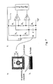
- FIG. 1 A preferred embodiment is represented in Fig. 1.
- a reactor vessel the top of which is provided with a precursor inlet (indicated with TEOS/O 2 ) through which supply of a precursor, a carrier gas and optionally oxygen can take place.
- the vessel wall is suitably provided with a grounding.
- Electrodes may be situated in the reactor space that is enclosed by the vessel.
- First and second plasmas may be provided a by means of a first and second plasma source.
- One of the electrodes may also be a carrier for a substrate.
- Zone I denotes the region of the first plasma, wherein particles are formed.
- Zone I is part of a plasma source that is delimited by a top plate and a separating mesh.
- the separating mesh is suspended from the top plate by way of a suspension device and is provided with a grounding, thereby also grounding the top plate.
- the first plasma source further comprises an electrode I in the form of a wire mesh (also termed “r.f. electrode mesh” herein) which is positioned in between the top plate and the separating mesh and which is provided with a radiofrequency (R.F.) charge.
- Electrode I is capable of discharging on both the separating mesh and the top plate.
- Precursors entering the first plasma source will become ionized in a plasma generated by said source and negative ions will become entrapped in the plasma thus generated in the region labeled Zone I of the first plasma source.
- the particles may fall through the separating mesh and reach the second plasma source.
- Zone II denotes the region of the second plasma wherein the matrix chemistry is formed.
- Zone II is part of a second plasma source that is delimited by the separating mesh described above for the first plasma source and by electrode II.
- Electrode II may function as the substrate carrier.
- This plasma source can be provided with its own precursor inlet (indicated byTMSE).
- the reactor may further be fitted with components that facilitate measurements to be performed on the plasmas (indicated by "OES” and "adjustable FTIR window” in Figure 1).
- the precursors, carrier gas and optionally oxygen will react in Zone I to create porous nanoparticles.
- these particulates are transported from Zone I to Zone II.
- the nanoparticles that reach Zone II will be combined with the matrix-forming chemistry produced in the second plasma, which plasma is produced as a result of ionization of precursors entering the inlet for the second plasma source and nanoparticles will be incorporated into the growing polymer layer.
- the substrate provided on the carrier is covered with a combination of both plasma products thus producing the coating on the substrate.
- the first plasma source is preferably a low electron density plasma. Further, the first plasma source is preferably a high-frequency plasma. More preferably the first plasma source is a CCP plasma..
- the second plasma source (if present) is preferably a low electron density plasma. Further, the second plasma source (if present) is preferably a high-frequency plasma. More preferably the second plasma source (if present) is a CCP plasma.
- both plasmas are CCP plasmas.
- a frequency of between 0.01 MHz and 10 GHz in this connection is very suitable for inducing discharge in the plasmas. It is greatly preferred that a frequency of between 1 and 50 MHz be used.
- the coupled plasmas applied are high-frequency plasmas.
- a frequency of between 0.01 MHz and 10 GHz in this connection is very suitable for inducing discharge in the plasmas. It is greatly preferred that a frequency of between 1 and 50 MHz be used.
- the plasmas can be situated in the direct vicinity of the substrate or at some distance therefrom.
- direct plasmas can still be used with great advantage in the present invention.
- At least one plasma source is situated at some distance from the substrate.
- Such "remote” plasmas therefore find particularly suitable application in the present invention.
- a device according to the invention be provided with transport means for a vapor phase.
- Such means can comprise "passive" means such as gravity, whereby the remote plasma, the substrate and the field of gravity are in one line.
- active transport means for a vapor phase can be included in a device according to the invention.
- Such active systems can consist of a pressure gradient or an active air, vapor or gas stream in the processing direction. 'Processing direction' as used herein is the direction in which a plasma-activated particle must travel to reach the substrate and to deposit thereon.
- An active air or gas stream can be generated by introducing air, vapor or gas with excess pressure into the device.
- a carrier gas such as N 2 , argon, or any other suitable unreactive gas, or a gas involved in the activation reaction, such as oxygen, can be used.
- an active air, vapor or gas stream can be generated by extracting air, vapor or gas from the device.
- the manner in which the pressure gradient or the active air, vapor or gas stream is obtained is not of preponderant importance in methods and devices of the invention.
- the transport means for a vapor phase are realized by introducing gas with excess pressure into the device and simultaneously extracting vapor from the device, so that a reduced pressure, with respect to atmospheric pressure, is created in the device. This further promotes a stable plasma discharge.
- a pressure between 0.01 and 1000 mbara finds suitable application in embodiments according to the present invention. Good results have been obtained at a pressure in the device between 0.1 and 50 mbara.
- the plasmas that can be used in the present invention are aimed at forming from precursor molecules, reactive intermediates that can be deposited on the substrate. Depending on the energy supplied to the plasma source, the precursor will be activated into a reacted and dissociated intermediate. The extent of dissociation can be set by choosing the level of the plasma source energy. Suitable powers in plasmas that are used in embodiments of the present invention are generally between 10 and 2500 Watts, with voltages varying between 0.001 and 5000 Volt.
- the plasma is pulsed to liberate the particles captured therein from the plasma volume and to effect deposition on the substrate to be coated.
- a pulse frequency of 1 to 100 Hz is used.
- a pulse of approximately 25 Hz is used.
- Concentrations of precursors in a plasma composition according to the invention are generally between 1 and 25 vol.%.
- oxygen can be supplied to the plasma composition to a concentration of approximately 80%.
- the plasma composition comprises an unreactive carrier gas such as N 2 or a noble gas such as argon, helium, neon, krypton, radon and/or xenon or a combination of these gases to supplement the volume.
- the plasma volume is preferably supplemented with argon gas.
- the formation of the inorganic precursor plasma is preferably effected by bringing the mixture of oxygen, precursor molecules and argon gas to electric discharge in a plasma source. The reactions thereby occurring lead to dissociation or activation of the precursor molecules.
- the activated intermediates Upon leaving the plasma, the activated intermediates preferably move substantially towards the substrate on which they can deposit and if possible substantially polymerize/condense.
- a considerable advantage of the present invention is that it is possible according to the proposed method to adjust the composition, and hence the properties of the low dielectric coating, to any desired specification or application.
- the ratio of inorganic to organic components, the density of the low dielectric material that is manufactured in this way and the amount of nanoparticles present can be fully controlled. In this way, many different specific properties can be imparted to the material. Also, to the different plasmas additives can be added, enabling specific properties to be imparted to a coating according to the invention.
- Suitable substrates for applying a coating according to the present invention are substrates generally used in the semiconductor industry, and may for instance include plastic, metal, glass and ceramics.
- the thickness of the coating can be adjusted by varying the vapor deposition time (the period in which the substrate is exposed to the chemical vapor phase). Thicker coatings are achieved after longer vapor deposition times.
- the deposition rate of the different activated components can be increased by supplying more energy to the plasmas or by increasing the gas or vapor stream through the device.
- the substrate can optionally be cleaned or otherwise treated to improve the adhesion of activated intermediates, and hence the entire coating.
- treatment methods are known in the art and comprise treatment with, for instance, HF, NH 4 OH or H 2 SO 4 , or with the aid of a plasma according to methods known for that purpose.
- a dual capacitive plasma reactor is used in combination with a process to synthesise nanoporous particles and simultaneously incorporate them into a silicone layer.
- the nanoporosity of these particles is used to introduce controlled porosity into the silicone layers with the aim of producing low- k lagers.
- Nanocomposite layers exhibiting dielectric constants of 1.82-1.86 have been demonstrated, compared to 3.05 for similar lagers without particle incorporation.
- the reactor design comprises two capacitively coupled plasma systems each connected to a power of 1 kW at 13.56 MHz supplied through matching networks (Fig. 1).
- the plasmas may or may not be pulsed, preferably they are pulsed.
- the precursors and gasses, e.g. TEOS and oxygen, for particle synthesis may be fed into Zone I, e.g. through the top inlet indicated, where they are activated by the plasma formed between the radio frequency (r.f.) electrode mesh (i.e. the mesh acting as electrode carrying a radio frequency current) and the top and bottom plates of the chamber defining Zone I.
- the radio frequency (r.f.) electrode mesh i.e. the mesh acting as electrode carrying a radio frequency current
- the self biasing of the r.f. electrode mesh acts to trap negative ions so that they may nucleate particle growth in this region.
- Both plasmas can be modulated so that particles trapped in Zone I can traverse the r.f. electrode mesh and flow into Zone II where they are combined with the polymer forming chemistry.
- a computational fluid dynamic (CFD) model of the particle forming region was made to identify recirculation or stagnation regions caused by the geometry (Fig. 2).
- the mesh electrode and grounded plate separating the two plasma regions have a open area of 38%.
- the skilled person will appreciate that proper selection of the open area will produce a more laminar flow at the substrate (Electrode II) and consequently a more homogenous film deposition profile.
- Particles were synthesized, trapped and monitored using a capacitively coupled r.f. discharge.
- a steel substrate table acted as the driven electrode and was surrounded by a grounded steel cage to contain the plasma.
- no cooling systems were implemented and the substrate typically reached a temperature of 100°C during film growth or particle synthesis which typically lasted about 10 minutes.
- Infrared spectroscopic measurements were done using a Midac M2500-C Fourier transform infrared spectrometer (FTIR) that consisted of two units.
- the detector unit housed the Mercury Cadmium Telluride (MCT) detector
- the source unit housed the Michelson interferometer and glow bar source.
- the tetraethoxysilane precursor [CAS 78-10-4] 98 % purity was evaporated and dosed using a Bronkhorst HiTec CEM system while argon and oxygen flows were controlled using Bronkhorst HiTec mass flow controllers. All gas lines to the reactor were heated to 80°C to prevent condensation of the TEOS precursor.
- a MKS throttle valve located in the reactor exhaust system regulated the reactor pressure, which was constant during each experiment.
- conditions for synthesis and trapping of particle were combined with conditions optimized for growing a-C:H layer.
- TGA Thermal gravimetric analysis
- Low- k films were synthesized using the combination of both the upstream (Zone I) and downstream (Zone II) plasmas.
- TEOS tetraethoxysilane
- Bronkhorst Hi-Tec CEM Controlled Evaporation and Mixing system (Bronkhorst, Ruurlo, The Netherlands) and combined with O 2 and Ar flows in the heated gas lines (80°C) and then fed into the upstream plasma.
- TMSE (1,2-bis[trimethylsilyloxy]ethane was dosed using a bubbler system using Ar as a carrier gas and fed via heated gas lines (80°C), into the downstream plasma.
- optical emission spectroscopy was performed by using an Ocean Optics USB-2000 spectrometer with a spectral range of between 280 to 800 mm and resolution of approximately 1 nm. Light from the reactor was fed into the optical emission spectroscopy (OES) spectrometer via an optical fiber. The concentration of O atoms in an Ar/O 2 plasma was monitored under various conditions using OES and an approach reported by Han et al . [31] and Lieberman [32].
- the plasmas were modulated with on and off times of 475 ms and 25 ms respectively to prevent particle trapping in the upstream plasma and above the substrate.
- a self-bias potential of 150 V was observed to develop on the substrate table.
- Depositions were performed using a deposition time of 5 minutes resulting in film thicknesses ranging from 0.88 to 2.04 ⁇ m depending on the precursor flows and discharge power. Film thicknesses were determined using a Tencor P-10 surface profiler with an estimated accuracy of approximately ⁇ 10 nm.
- Boron doped silicon wafers with a resistivity of between 7 and 21 ohm cm were placed in the centre of the r.f. biased substrate table and used as substrates for determining the dielectric constants. All substrates were used as delivered and no attempt was made to clean or remove the native oxide.
- the dielectric constants are determined from measurements of the materials capacitance using two independent methods described in Section on Dielectric Constant Determination hereinbelow.
- the dielectric constant of a material is affected by the material composition and porosity as discussed in the introduction to this chapter. The influence of both these phenomena on the dielectric constant can be seen in Fig. 5.
- Increasing the r.f. bias potential. (Fig. 5a) is known to enhance film density by increasing the energy of ions bombarding the film surface.
- the subsequent drop in porosity caused the dielectric constant to increase.
- Films deposited under identical conditions both without the TEOS/O 2 particle plasma (Fig 5a) exhibit much higher k values indicating that the lower k values observed for the nanocomposite films is indeed due to the incorporation of porous particles.
- the effect of film composition on the dielectric constant is such that at low oxygen concentrations silicone-like particles are produced retaining some of the organic functionality of the original TEOS precursor. As the oxygen concentration in the particle-forming plasma increases, so does the inorganic nature of the particles. Inorganic materials are characterised by polar bonding, this increases the concentration of permanent dipoles present in the film.
- Method A 1 cm 2 samples are prepared from the Si substrate and sputtered with a 60 nm gold front contact layer. Silver paint is applied to the backside of the sample to ensure a good electrical contact to the silicon wafer. The sample is then mounted between two contacts and connected to the Hewlett Packard 4284A Precision LCR meter (20 Hz to 1 MHz) (Fig. 10) and the capacitance measured at 1 kHz and 1 MHz oscillating potentials of 50 and 100 mV.
- Method B A contact pattern of aluminium is sputtered onto the top of the sample as shown in Fig. 11a and 11b.
- the sample is then placed into an oscillating circuit consisting of two comparators and a flip-flop reset switch (Fig. 11c).
- the negative and positive inputs of comparators one and two ( Cp 1 - and Cp 2 +) are set at 1/3 and 2/3 the line voltage respectively, by R 2 .
- the other two comparator inputs ( Cp 1 + and Cp 2 -) are charge via resistors R 4 and R 5 until the comparator outputs switch and the flip-flop and transistor grounds the comparator inputs ( Cp 1 + and Cp 2 -) and resets the circuit.
- d is the thickness of the dielectric layer [m] with permittivity ⁇ r
- ⁇ 0 is the permittivity of free space [Fm -1 ].
- the oscillating frequency is determined by R 4 , R 5 and C.
- the presence of internal and parasitic capacitance are accounted for by calibrating the circuit resonant frequencies with a series of fixed capacitors (1 % tolerance).
- Errors in the dielectric constant measurements are predominantly caused by the uncertainty in the film thickness and uniformity and are estimated to be approximately 2-6 %.
- Method B is likely to be less reliable than A for several reasons namely,
Landscapes
- Chemical & Material Sciences (AREA)
- Engineering & Computer Science (AREA)
- Materials Engineering (AREA)
- Organic Chemistry (AREA)
- Mechanical Engineering (AREA)
- Chemical Kinetics & Catalysis (AREA)
- Physics & Mathematics (AREA)
- Metallurgy (AREA)
- General Chemical & Material Sciences (AREA)
- Nanotechnology (AREA)
- Crystallography & Structural Chemistry (AREA)
- General Physics & Mathematics (AREA)
- Inorganic Chemistry (AREA)
- Condensed Matter Physics & Semiconductors (AREA)
- Wood Science & Technology (AREA)
- Life Sciences & Earth Sciences (AREA)
- Composite Materials (AREA)
- Plasma & Fusion (AREA)
- Chemical Vapour Deposition (AREA)
- Formation Of Insulating Films (AREA)
Priority Applications (4)
| Application Number | Priority Date | Filing Date | Title |
|---|---|---|---|
| EP04076150A EP1586674A1 (fr) | 2004-04-14 | 2004-04-14 | Procédé et méthode de dépot de couches |
| US11/578,491 US8230807B2 (en) | 2004-04-14 | 2005-04-14 | Coatings, and methods and devices for the manufacture thereof |
| PCT/NL2005/000279 WO2005100633A1 (fr) | 2004-04-14 | 2005-04-14 | Revetements, procedes et dispositifs de fabrication associes |
| JP2007508290A JP4860603B2 (ja) | 2004-04-14 | 2005-04-14 | コーティング、並びにそれを製造するための方法及び装置 |
Applications Claiming Priority (1)
| Application Number | Priority Date | Filing Date | Title |
|---|---|---|---|
| EP04076150A EP1586674A1 (fr) | 2004-04-14 | 2004-04-14 | Procédé et méthode de dépot de couches |
Publications (1)
| Publication Number | Publication Date |
|---|---|
| EP1586674A1 true EP1586674A1 (fr) | 2005-10-19 |
Family
ID=34928157
Family Applications (1)
| Application Number | Title | Priority Date | Filing Date |
|---|---|---|---|
| EP04076150A Withdrawn EP1586674A1 (fr) | 2004-04-14 | 2004-04-14 | Procédé et méthode de dépot de couches |
Country Status (4)
| Country | Link |
|---|---|
| US (1) | US8230807B2 (fr) |
| EP (1) | EP1586674A1 (fr) |
| JP (1) | JP4860603B2 (fr) |
| WO (1) | WO2005100633A1 (fr) |
Cited By (6)
| Publication number | Priority date | Publication date | Assignee | Title |
|---|---|---|---|---|
| US20110005352A1 (en) * | 2008-03-04 | 2011-01-13 | National Institute of Advanced Science and Technol ogy | Method of Producing Inorganic Nanoparticles in Atmosphere and Device Therefor |
| EP2382063A1 (fr) * | 2008-12-24 | 2011-11-02 | Intrinsiq Materials Limited | Particules fines |
| EP1937225A4 (fr) * | 2005-08-12 | 2012-02-22 | Procter & Gamble | Substrat revêtu des propriétés d'un tissu kératinique |
| WO2014184566A1 (fr) * | 2013-05-17 | 2014-11-20 | Surface Innovations Limited | Procédé de formation de nanocomposites polymères dans des jonctions entre substrats |
| WO2021123759A1 (fr) * | 2019-12-17 | 2021-06-24 | University Of Surrey | Dépôt de film mince amélioré par plasma à l'aide d'une injection de précurseur liquide |
| CN115433480A (zh) * | 2022-10-21 | 2022-12-06 | 广东华葆新材料科技有限公司 | 一种基于硅酸锂的防静电墙面无机涂料及其制备方法 |
Families Citing this family (29)
| Publication number | Priority date | Publication date | Assignee | Title |
|---|---|---|---|---|
| US8124207B2 (en) * | 2004-03-02 | 2012-02-28 | Sakhrani Vinay G | Article with lubricated surface and method |
| US9540562B2 (en) * | 2004-05-13 | 2017-01-10 | Baker Hughes Incorporated | Dual-function nano-sized particles |
| US7470466B2 (en) | 2005-12-23 | 2008-12-30 | Boston Scientific Scimed, Inc. | Nanoparticle structures and composite materials comprising a silicon-containing compound having a chemical linker that forms a non-covalent bond with a polymer |
| US8455088B2 (en) | 2005-12-23 | 2013-06-04 | Boston Scientific Scimed, Inc. | Spun nanofiber, medical devices, and methods |
| US8084103B2 (en) * | 2006-08-15 | 2011-12-27 | Sakhrani Vinay G | Method for treating a hydrophilic surface |
| FR2905708B1 (fr) * | 2006-09-07 | 2008-12-05 | Commissariat Energie Atomique | Substrat de culture pourvu d'un revetement en silicone oxydee |
| BRPI0720867A2 (pt) * | 2006-12-29 | 2014-03-04 | 3M Innovative Properties Company. | Método para fabricação de filmes inorgânicos ou híbridos inorgânicos/orgânicos |
| CN101573471A (zh) * | 2006-12-29 | 2009-11-04 | 3M创新有限公司 | 固化含有金属烷氧化物的膜的方法 |
| CN101971298A (zh) | 2007-11-02 | 2011-02-09 | 佳能安内华股份有限公司 | 表面处理设备和表面处理方法 |
| JP5425404B2 (ja) * | 2008-01-18 | 2014-02-26 | 東京エレクトロン株式会社 | アモルファスカーボン膜の処理方法およびそれを用いた半導体装置の製造方法 |
| US8088451B2 (en) * | 2008-03-13 | 2012-01-03 | Board Of Regents, The University Of Texas System | Covalently functionalized particles for synthesis of new composite materials |
| US8470459B2 (en) * | 2008-03-25 | 2013-06-25 | The Curators Of The University Of Missouri | Nanocomposite dielectric coatings |
| EP2332164A1 (fr) * | 2008-09-03 | 2011-06-15 | Dow Corning Corporation | Réacteur à plasma pulsé à haute fréquence sous faible pression permettant de produire des nanoparticules |
| CA2747209A1 (fr) * | 2008-12-17 | 2010-06-24 | University Of South Australia | Films polymeres actifs |
| JPWO2010082345A1 (ja) * | 2009-01-19 | 2012-06-28 | 日新電機株式会社 | シリコンドット形成方法及びシリコンドット形成装置 |
| US20110111132A1 (en) * | 2009-11-09 | 2011-05-12 | Electric Power Research Institute, Inc. | System and method for depositing coatings on inner surface of tubular structure |
| CN102986020A (zh) * | 2010-06-30 | 2013-03-20 | 康宁股份有限公司 | 对绝缘体基材上的硅进行精整的方法 |
| JP5781350B2 (ja) * | 2011-03-30 | 2015-09-24 | リンテック株式会社 | ガスバリア積層体、その製造方法、電子デバイス用部材及び電子デバイス |
| US9133412B2 (en) | 2012-07-09 | 2015-09-15 | Tribofilm Research, Inc. | Activated gaseous species for improved lubrication |
| FR2995999B1 (fr) * | 2012-09-27 | 2014-10-17 | Centre Nat Rech Scient | Methode et systeme de detection et/ou d'analyse de particules dans un plasma froid |
| DE102013112855A1 (de) * | 2013-11-21 | 2015-05-21 | Aixtron Se | Vorrichtung und Verfahren zum Fertigen von aus Kohlenstoff bestehenden Nanostrukturen |
| US9727672B2 (en) * | 2015-02-26 | 2017-08-08 | Uchicago Argonne, Llc | Fast method for reactor and feature scale coupling in ALD and CVD |
| US9659788B2 (en) * | 2015-08-31 | 2017-05-23 | American Air Liquide, Inc. | Nitrogen-containing compounds for etching semiconductor structures |
| US20180025889A1 (en) * | 2016-07-22 | 2018-01-25 | Regents Of The University Of Minnesota | Nonthermal plasma synthesis |
| CN106929821B (zh) * | 2017-01-17 | 2019-12-20 | 复旦大学 | 一种金属含量可调的金属氮化物薄膜的制备方法及反应器 |
| US11686671B2 (en) * | 2018-10-26 | 2023-06-27 | Fujikin Incorporated | Concentration measurement device |
| TWI756742B (zh) * | 2019-07-09 | 2022-03-01 | 日商住友重機械工業股份有限公司 | 負離子生成裝置 |
| CN113943933B (zh) * | 2020-07-16 | 2023-09-29 | 江苏菲沃泰纳米科技股份有限公司 | 多层结构的复合膜及其制备方法和产品 |
| CN116254518B (zh) * | 2023-05-10 | 2023-08-18 | 上海陛通半导体能源科技股份有限公司 | 氮化硅薄膜的制备方法 |
Citations (5)
| Publication number | Priority date | Publication date | Assignee | Title |
|---|---|---|---|---|
| EP0443400A1 (fr) * | 1990-02-21 | 1991-08-28 | Rogers Corporation | Matériel composite diélectrique |
| JP2000021245A (ja) * | 1998-07-02 | 2000-01-21 | Jsr Corp | 低誘電体形成材料および低誘電体 |
| KR20030023964A (ko) * | 2001-09-14 | 2003-03-26 | 주성엔지니어링(주) | 리모트 플라즈마를 이용하는 ccp형 pecvd장치 |
| WO2003066933A1 (fr) * | 2002-01-18 | 2003-08-14 | Nederlandse Organisatie Voor Toegepast-Natuurwetenschappelijk Onderzoek Tno | Procede de depot de films inorganiques/organiques |
| US6660391B1 (en) * | 1998-04-28 | 2003-12-09 | Asml Us, Inc. | Low κ dielectric inorganic/organic hybrid films and method of making |
Family Cites Families (5)
| Publication number | Priority date | Publication date | Assignee | Title |
|---|---|---|---|---|
| US5024927A (en) * | 1988-10-06 | 1991-06-18 | Ricoh Company, Ltd. | Information recording medium |
| KR100197649B1 (ko) * | 1995-09-29 | 1999-06-15 | 김영환 | 박막 증착장치 |
| US6126778A (en) * | 1998-07-22 | 2000-10-03 | Micron Technology, Inc. | Beat frequency modulation for plasma generation |
| JP3366301B2 (ja) * | 1999-11-10 | 2003-01-14 | 日本電気株式会社 | プラズマcvd装置 |
| KR100458779B1 (ko) * | 2000-03-27 | 2004-12-03 | 미츠비시 쥬고교 가부시키가이샤 | 금속막의 제작방법 및 그 제작장치 |
-
2004
- 2004-04-14 EP EP04076150A patent/EP1586674A1/fr not_active Withdrawn
-
2005
- 2005-04-14 US US11/578,491 patent/US8230807B2/en active Active
- 2005-04-14 WO PCT/NL2005/000279 patent/WO2005100633A1/fr not_active Ceased
- 2005-04-14 JP JP2007508290A patent/JP4860603B2/ja not_active Expired - Lifetime
Patent Citations (5)
| Publication number | Priority date | Publication date | Assignee | Title |
|---|---|---|---|---|
| EP0443400A1 (fr) * | 1990-02-21 | 1991-08-28 | Rogers Corporation | Matériel composite diélectrique |
| US6660391B1 (en) * | 1998-04-28 | 2003-12-09 | Asml Us, Inc. | Low κ dielectric inorganic/organic hybrid films and method of making |
| JP2000021245A (ja) * | 1998-07-02 | 2000-01-21 | Jsr Corp | 低誘電体形成材料および低誘電体 |
| KR20030023964A (ko) * | 2001-09-14 | 2003-03-26 | 주성엔지니어링(주) | 리모트 플라즈마를 이용하는 ccp형 pecvd장치 |
| WO2003066933A1 (fr) * | 2002-01-18 | 2003-08-14 | Nederlandse Organisatie Voor Toegepast-Natuurwetenschappelijk Onderzoek Tno | Procede de depot de films inorganiques/organiques |
Non-Patent Citations (2)
| Title |
|---|
| DATABASE WPI Section EI Week 200348, Derwent World Patents Index; Class U11, AN 2003-511373, XP002298710 * |
| PATENT ABSTRACTS OF JAPAN vol. 2000, no. 04 31 August 2000 (2000-08-31) * |
Cited By (8)
| Publication number | Priority date | Publication date | Assignee | Title |
|---|---|---|---|---|
| EP1937225A4 (fr) * | 2005-08-12 | 2012-02-22 | Procter & Gamble | Substrat revêtu des propriétés d'un tissu kératinique |
| US20110005352A1 (en) * | 2008-03-04 | 2011-01-13 | National Institute of Advanced Science and Technol ogy | Method of Producing Inorganic Nanoparticles in Atmosphere and Device Therefor |
| US8512437B2 (en) * | 2008-03-04 | 2013-08-20 | National Institute Of Advanced Industrial Science And Technology | Method of producing inorganic nanoparticles in atmosphere and device therefor |
| EP2382063A1 (fr) * | 2008-12-24 | 2011-11-02 | Intrinsiq Materials Limited | Particules fines |
| WO2014184566A1 (fr) * | 2013-05-17 | 2014-11-20 | Surface Innovations Limited | Procédé de formation de nanocomposites polymères dans des jonctions entre substrats |
| WO2021123759A1 (fr) * | 2019-12-17 | 2021-06-24 | University Of Surrey | Dépôt de film mince amélioré par plasma à l'aide d'une injection de précurseur liquide |
| US20230067839A1 (en) * | 2019-12-17 | 2023-03-02 | University Of Surrey | Plasma enhanced thin film deposition using liquid precursor injection |
| CN115433480A (zh) * | 2022-10-21 | 2022-12-06 | 广东华葆新材料科技有限公司 | 一种基于硅酸锂的防静电墙面无机涂料及其制备方法 |
Also Published As
| Publication number | Publication date |
|---|---|
| US20080038484A1 (en) | 2008-02-14 |
| WO2005100633A1 (fr) | 2005-10-27 |
| US8230807B2 (en) | 2012-07-31 |
| JP2007532781A (ja) | 2007-11-15 |
| JP4860603B2 (ja) | 2012-01-25 |
Similar Documents
| Publication | Publication Date | Title |
|---|---|---|
| EP1586674A1 (fr) | Procédé et méthode de dépot de couches | |
| US7112615B2 (en) | Porous material formation by chemical vapor deposition onto colloidal crystal templates | |
| US6716770B2 (en) | Low dielectric constant material and method of processing by CVD | |
| US8178170B2 (en) | Method for depositing inorganic/organic films | |
| KR100907387B1 (ko) | 환원 분위기 하에서 유전 필름을 경화시키는 방법 | |
| KR100437068B1 (ko) | 탄소질 산화실리콘의 형성방법 | |
| CN109166787B (zh) | 一种氧化硅薄膜的可流动化学气相沉积方法 | |
| KR20000068308A (ko) | 반도체기판상에평탄한유전체층을침전시키는장치및방법 | |
| JP4881153B2 (ja) | 水素化シリコンオキシカーバイド膜の生成方法。 | |
| CN101743247A (zh) | 利用等离子体增强化学气相沉积来制造高机械性能的极低k膜的新型硅前驱物 | |
| EP1428906A1 (fr) | Matériau à faible constante diélectrique et procédé CVD | |
| CN1698189A (zh) | 改善低介电常数材料的破裂临界值及机械特性的方法 | |
| CN101671816A (zh) | 含Si膜的沉积方法,绝缘体膜,和半导体器件 | |
| KR101881534B1 (ko) | 플라즈마를 이용한 금속산화물이 포함된 탄소막의 형성 방법 | |
| JPH05102040A (ja) | 成膜方法 | |
| Lee et al. | Effect of annealing temperature on dielectric constant and bonding structure of low-k SiCOH thin films deposited by plasma enhanced chemical vapor deposition | |
| KR101157683B1 (ko) | 실리콘 산화막의 제조 방법 | |
| Sahli et al. | Deposition of SiO2-like films by HMDSN/O2 plasmas at low pressure in a MMP-DECR reactor | |
| US8105661B2 (en) | Method for forming porous insulation film | |
| JP2001196365A (ja) | 成膜方法、成膜装置及び半導体装置の製造方法 | |
| JP4618086B2 (ja) | Si含有膜及びその製造方法等 | |
| US20160024267A1 (en) | Porous film with high hardness and a low dielectric constant and preparation method thereof | |
| Cho et al. | A low dielectric study on hybrid plasma-polymer thin films of different ratio between toluene and TEOS |
Legal Events
| Date | Code | Title | Description |
|---|---|---|---|
| PUAI | Public reference made under article 153(3) epc to a published international application that has entered the european phase |
Free format text: ORIGINAL CODE: 0009012 |
|
| AK | Designated contracting states |
Kind code of ref document: A1 Designated state(s): AT BE BG CH CY CZ DE DK EE ES FI FR GB GR HU IE IT LI LU MC NL PL PT RO SE SI SK TR |
|
| AX | Request for extension of the european patent |
Extension state: AL HR LT LV MK |
|
| AKX | Designation fees paid | ||
| REG | Reference to a national code |
Ref country code: DE Ref legal event code: 8566 |
|
| STAA | Information on the status of an ep patent application or granted ep patent |
Free format text: STATUS: THE APPLICATION IS DEEMED TO BE WITHDRAWN |
|
| 18D | Application deemed to be withdrawn |
Effective date: 20060420 |