EP1586939A1 - Ecran a cristaux liquides - Google Patents
Ecran a cristaux liquides Download PDFInfo
- Publication number
- EP1586939A1 EP1586939A1 EP04771476A EP04771476A EP1586939A1 EP 1586939 A1 EP1586939 A1 EP 1586939A1 EP 04771476 A EP04771476 A EP 04771476A EP 04771476 A EP04771476 A EP 04771476A EP 1586939 A1 EP1586939 A1 EP 1586939A1
- Authority
- EP
- European Patent Office
- Prior art keywords
- liquid crystal
- refractive index
- retardation film
- thickness
- light
- Prior art date
- Legal status (The legal status is an assumption and is not a legal conclusion. Google has not performed a legal analysis and makes no representation as to the accuracy of the status listed.)
- Withdrawn
Links
Images

















Classifications
-
- G—PHYSICS
- G02—OPTICS
- G02F—OPTICAL DEVICES OR ARRANGEMENTS FOR THE CONTROL OF LIGHT BY MODIFICATION OF THE OPTICAL PROPERTIES OF THE MEDIA OF THE ELEMENTS INVOLVED THEREIN; NON-LINEAR OPTICS; FREQUENCY-CHANGING OF LIGHT; OPTICAL LOGIC ELEMENTS; OPTICAL ANALOGUE/DIGITAL CONVERTERS
- G02F1/00—Devices or arrangements for the control of the intensity, colour, phase, polarisation or direction of light arriving from an independent light source, e.g. switching, gating or modulating; Non-linear optics
- G02F1/01—Devices or arrangements for the control of the intensity, colour, phase, polarisation or direction of light arriving from an independent light source, e.g. switching, gating or modulating; Non-linear optics for the control of the intensity, phase, polarisation or colour
- G02F1/13—Devices or arrangements for the control of the intensity, colour, phase, polarisation or direction of light arriving from an independent light source, e.g. switching, gating or modulating; Non-linear optics for the control of the intensity, phase, polarisation or colour based on liquid crystals, e.g. single liquid crystal display cells
- G02F1/133—Constructional arrangements; Operation of liquid crystal cells; Circuit arrangements
- G02F1/1333—Constructional arrangements; Manufacturing methods
- G02F1/1335—Structural association of cells with optical devices, e.g. polarisers or reflectors
- G02F1/13363—Birefringent elements, e.g. for optical compensation
- G02F1/133634—Birefringent elements, e.g. for optical compensation the refractive index Nz perpendicular to the element surface being different from in-plane refractive indices Nx and Ny, e.g. biaxial or with normal optical axis
-
- G—PHYSICS
- G02—OPTICS
- G02F—OPTICAL DEVICES OR ARRANGEMENTS FOR THE CONTROL OF LIGHT BY MODIFICATION OF THE OPTICAL PROPERTIES OF THE MEDIA OF THE ELEMENTS INVOLVED THEREIN; NON-LINEAR OPTICS; FREQUENCY-CHANGING OF LIGHT; OPTICAL LOGIC ELEMENTS; OPTICAL ANALOGUE/DIGITAL CONVERTERS
- G02F1/00—Devices or arrangements for the control of the intensity, colour, phase, polarisation or direction of light arriving from an independent light source, e.g. switching, gating or modulating; Non-linear optics
- G02F1/01—Devices or arrangements for the control of the intensity, colour, phase, polarisation or direction of light arriving from an independent light source, e.g. switching, gating or modulating; Non-linear optics for the control of the intensity, phase, polarisation or colour
- G02F1/13—Devices or arrangements for the control of the intensity, colour, phase, polarisation or direction of light arriving from an independent light source, e.g. switching, gating or modulating; Non-linear optics for the control of the intensity, phase, polarisation or colour based on liquid crystals, e.g. single liquid crystal display cells
- G02F1/133—Constructional arrangements; Operation of liquid crystal cells; Circuit arrangements
- G02F1/1333—Constructional arrangements; Manufacturing methods
- G02F1/1335—Structural association of cells with optical devices, e.g. polarisers or reflectors
- G02F1/13363—Birefringent elements, e.g. for optical compensation
-
- G—PHYSICS
- G02—OPTICS
- G02B—OPTICAL ELEMENTS, SYSTEMS OR APPARATUS
- G02B5/00—Optical elements other than lenses
- G02B5/30—Polarising elements
-
- G—PHYSICS
- G02—OPTICS
- G02B—OPTICAL ELEMENTS, SYSTEMS OR APPARATUS
- G02B5/00—Optical elements other than lenses
- G02B5/30—Polarising elements
- G02B5/3083—Birefringent or phase retarding elements
-
- G—PHYSICS
- G02—OPTICS
- G02F—OPTICAL DEVICES OR ARRANGEMENTS FOR THE CONTROL OF LIGHT BY MODIFICATION OF THE OPTICAL PROPERTIES OF THE MEDIA OF THE ELEMENTS INVOLVED THEREIN; NON-LINEAR OPTICS; FREQUENCY-CHANGING OF LIGHT; OPTICAL LOGIC ELEMENTS; OPTICAL ANALOGUE/DIGITAL CONVERTERS
- G02F1/00—Devices or arrangements for the control of the intensity, colour, phase, polarisation or direction of light arriving from an independent light source, e.g. switching, gating or modulating; Non-linear optics
- G02F1/01—Devices or arrangements for the control of the intensity, colour, phase, polarisation or direction of light arriving from an independent light source, e.g. switching, gating or modulating; Non-linear optics for the control of the intensity, phase, polarisation or colour
- G02F1/13—Devices or arrangements for the control of the intensity, colour, phase, polarisation or direction of light arriving from an independent light source, e.g. switching, gating or modulating; Non-linear optics for the control of the intensity, phase, polarisation or colour based on liquid crystals, e.g. single liquid crystal display cells
- G02F1/133—Constructional arrangements; Operation of liquid crystal cells; Circuit arrangements
- G02F1/1333—Constructional arrangements; Manufacturing methods
- G02F1/1337—Surface-induced orientation of the liquid crystal molecules, e.g. by alignment layers
- G02F1/133749—Surface-induced orientation of the liquid crystal molecules, e.g. by alignment layers for low pretilt angles, i.e. lower than 15 degrees
-
- G—PHYSICS
- G02—OPTICS
- G02F—OPTICAL DEVICES OR ARRANGEMENTS FOR THE CONTROL OF LIGHT BY MODIFICATION OF THE OPTICAL PROPERTIES OF THE MEDIA OF THE ELEMENTS INVOLVED THEREIN; NON-LINEAR OPTICS; FREQUENCY-CHANGING OF LIGHT; OPTICAL LOGIC ELEMENTS; OPTICAL ANALOGUE/DIGITAL CONVERTERS
- G02F1/00—Devices or arrangements for the control of the intensity, colour, phase, polarisation or direction of light arriving from an independent light source, e.g. switching, gating or modulating; Non-linear optics
- G02F1/01—Devices or arrangements for the control of the intensity, colour, phase, polarisation or direction of light arriving from an independent light source, e.g. switching, gating or modulating; Non-linear optics for the control of the intensity, phase, polarisation or colour
- G02F1/13—Devices or arrangements for the control of the intensity, colour, phase, polarisation or direction of light arriving from an independent light source, e.g. switching, gating or modulating; Non-linear optics for the control of the intensity, phase, polarisation or colour based on liquid crystals, e.g. single liquid crystal display cells
- G02F1/133—Constructional arrangements; Operation of liquid crystal cells; Circuit arrangements
- G02F1/1333—Constructional arrangements; Manufacturing methods
- G02F1/1343—Electrodes
- G02F1/134309—Electrodes characterised by their geometrical arrangement
- G02F1/134363—Electrodes characterised by their geometrical arrangement for applying an electric field parallel to the substrate, i.e. in-plane switching [IPS]
Definitions
- the present invention relates to a liquid crystal display device including a pair of polarization plates each formed from a polarizer and a pair of protective layers that protect the polarizer between them, the polarizers being laid orthogonal to each other, and a liquid crystal layer disposed between the polarization plates to have the molecules thereof aligned parallel with the absorption axis of one of the polarization plates.
- the liquid crystal display device is widely used as a variety of display means incorporated in an OA (office automation) device such as a word processor, personal computer or the like, and as a television set, car navigation monitor, aircraft-cockpit monitor or the like because of being advantageous in that it can be connected directly to an IC because of the operability with a low voltage and small power consumption, has many displaying functions, and can easily be designed lightweight and compact.
- OA office automation
- the liquid crystal display device uses the polarization plates to visualize a change of liquid crystal alignment.
- the polarization plate normally includes a polarizer and transparent protective films made of triacetyl cellulose (TAC) laminated over both sides of the polarizer.
- TAC triacetyl cellulose
- the polarizer is an optical element that splits incident light into two polarized components orthogonal to each other, and passes only one of the two polarized components (component which oscillates in a direction parallel with the transmission axis of the polarizer) while absorbing or dispersing the other component (component which oscillates in a direction parallel with the absorption axis of the polarizer).
- the transmission type liquid crystal display device includes a liquid crystal cell which is sandwiched between polarization plates in its direction of thickness.
- the polarizers included in the opposite polarization plates, respectively, are normally disposed with their transmission axes being orthogonal to each other.
- the pair of polarizers whose transmission axes are orthogonal to each other is called "orthogonal polarizer".
- the characteristic of the polarizer depends upon the viewing angle. Namely, when light is incident obliquely upon the polarizer, the transmission axis varies in direction.
- the crossed-axes angle in relation to oblique incident light will not be the right angle, so that polarized light having passed through the first polarizer will have components parallel with the transmission axis of the second polarizer and which will pass through the second polarizer, resulting in light leakage.
- IPS in-plane switching
- the polarization plate is formed from a polarizer that passes predetermined-directional light and a protective layer laminated on either side of the polarizer.
- the protective layer is made of TAC or the like and the polarizer is sandwiched between the protective layers in the direction of thickness. Therefore, incident light having passed through the polarizer will pass through the protective layer interposed between the polarizer and liquid crystal cell, and arrive at a liquid crystal layer.
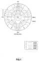
- FIG. 1 shows a viewing angle when the display screen will have the black level.
- the absorption axis of the lower polarization plate (at the side of the back light) is set at an angle of 90 deg.
- absorption axis of the upper polarization plate is to an angle of 0 deg.
- liquid crystal is aligned at an azimuth of 90 deg. (in which the alignment direction is open through 90 deg. on a lower substrate), and the substrate is pretilted at an angle of 2 deg.
- the light path length difference ⁇ nd LC of the liquid crystal layer is set to 275 nm (when light used has a wavelength of 550 nm).
- the protective layer included in the polarization plate is made of TAC and functions as a uniaxial retardation film having an optical axis perpendicular to the substrate.
- the light path length difference ⁇ nd TAC0 of each protective layer interposed between the polarizers in the upper and lower polarization plates and the liquid crystal layer is 50 nm.
- each of letters a , to e shows an isoluminance contour plotted by a value of the ratio between incident light and leakage light, also shown. As will be seen, a large light transmission takes place in a direction of 45 deg.
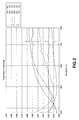
- FIG. 2 shows spectral transmittances at the time of a black-level display in the conventional liquid crystal display device when the display screen is viewed at an angle Pola (elevation angle) of 70 deg. and each of azimuths Azim of 15, 30, 45, 60 and 75 deg.
- FIG. 3 shows spectral transmittances at the time of a black-level display in the conventional liquid crystal display device when the display screen is viewed at an angle Pola (elevation angle) of 70 deg. and each of azimuths Azim of 345, 330, 315, 300 and 285 deg.
- the azimuth Azim is a counterclockwise angle from a viewing angle of 0 deg. from the right in the drawings.
- the light transmittance is high and the spectral transmittance provides a yellowish display, resulting in a lower quality of display.
- Japanese Unexamined Patent Application Publication discloses the use of a biaxial retardation film for optical compensation of the polarizers, but not any interposition of a protective layer having a negative phase difference between the polarizer in the polarization plate and the liquid crystal layer. It does not disclose the use of any in-plane switching mode liquid crystal layer with the protective layer interposed as above. Therefore, even with the use of the technology disclosed in the Japanese Unexamined Patent Application Publication, it is difficult to overcome the problem of the lower display quality and compensate the dependence of the polarizer upon the viewing angle.
- the present invention has an object to overcome the above-mentioned drawbacks of the related art by providing a liquid crystal display device including a pair of polarization plates each formed from a polarizer and a pair of protective layers that protect the polarizer, the polarizers being laid orthogonal to each other, and a crystal layer disposed between the pair of polarization plates to have the molecules thereof aligned parallel with the direction of the absorption axis of one of the polarization plates, for example, a so-called in-plane switching (IPS) mode type liquid crystal display device in which the liquid crystal molecules are activated by a field parallel to a substrate, in which especially in case for polarization plates each including protective layers having a negative phase difference and interposed between polarizers and a liquid crystal layer, there is provided a retardation film optimized for the negative phase difference by making optical compensation for an improved viewing angle for a black-level display.
- IPS in-plane switching
- a liquid crystal display device including a pair of polarization plates each formed from a polarizer and a pair of protective layers laminated over the polarizer to protect the latter, the transmission axes of the polarizers being orthogonal to each other, and a liquid crystal plate disposed between the polarization plates and including a liquid crystal layer having the molecules thereof aligned parallel with the absorption axis of one of the polarization plates, wherein:
- the biaxial retardation film is directed to vary in refractive index in the plane perpendicular to the direction of its thickness and show a maximum refractive index nx in that plane; and with the refractive index in a direction perpendicular, in the plane, to the direction to show the maximum refractive index nx being taken as ny, a product of the difference (nx - ny) between the refractive indexes nx and ny and the thickness of the retardation film being taken as an in-plane light path length difference of the retardation film, and with a product of the difference between the thickness-directional refractive index and in-plane-directional one, of the protective layer and the thickness of the protective layer being taken as a light path length difference of the protective layer, the in-plane light path length difference of the retardation film is set with a predetermined wavelength in a visible domain on the basis of the light path length difference of the protective layer and predetermined wavelength to compensate the dependence
- a liquid crystal display device including a pair of polarization plates each formed from a polarizer whose transmission axis is orthogonal to that of a polarizer in the other polarization plate and a liquid crystal plate disposed between the polarization plates and including a liquid crystal layer having the molecules thereof aligned parallel with the absorption axis of one of the polarization plates, wherein:
- the first retardation film By setting, by the first retardation film, the in-plane light path length difference to that before the incident passes through the liquid crystal layer and changing the polarization of the light through 180 deg. by the second retardation film whose in-plane light path length difference is about ⁇ /2, to thereby cancel the polarization by one of the pair of protective layers equal in thickness to each other by the polarization by the other protective layer, it is possible to maintain the black-level display independently of any viewing angle.
- the first retardation film should preferably be a biaxial one, or a negative uniaxial one, having a predetermined light path length difference.
- the present invention is applied, for example, to a liquid crystal display device 100 configured as shown in FIG. 4.
- a liquid crystal display device 100 configured as shown in FIG. 4.
- members governing the black-level transmittance are shown in simplified forms, respectively, in FIG. 4.
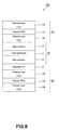
- the liquid crystal display device 100 includes a pair of polarization plates 10A and 10B disposed with their transmission axes being laid orthogonal to each other, and a crystal plate 20 including a liquid crystal layer 21 disposed parallel to the absorption axis of one of the polarization plates.
- the polarization plate 10A includes a polarizer 11A and protective layers 12A and 13A which protect the polarizer 11A, and the polarization plate 10B in pair with the polarization plate 10A includes a polarizer 11B being in pair with the polarization 11A and whose transmission axis is orthogonal to that of the polarizer 11A and protective layers 12B and 13B which protect the polarizer 11B.
- the liquid crystal plate 20 includes the liquid crystal layer 21 disposed parallel with the absorption axis of one of the polarization plates and glass substrates 22 and 23 having the liquid crystal layer 21 sealed between them.
- the liquid crystal plate 20 forms the so-called in-plane switching (IPS) mode type liquid crystal display device 100 in which liquid crystal molecules are activated by a field parallel to the glass substrates 22 and 23.
- IPS in-plane switching
- any azimuth is specifically referred to with respect to the polarization axis of the polarization plate, it shall be taken as an azimuth of 45, 135, 225 or 315 deg. in the following description.
- the polarization plates 10 include the polarizers 11 formed from a drawn PVA (polyvinyl alcohol) film on which iodine or the like is applied by adsorption and protective layers 12 and 13 formed from TAC (triacetyl cellulose) and which hold the polarizer 11 sandwiched between them.
- the polarization plate may be considered as combination of an O-type polarizer which absorbs light in a direction for an abnormal light refractive index and a negative retardation film whose optical axis is perpendicular to the substrate.
- the liquid crystal layer 21 in the black display state in the IPS mode can be considered as a uniaxial retardation film. Generally, it functions as a ⁇ /2 plate with a predetermined wavelength of green (G) light. That is to say, a model in the black display state in case a liquid crystal display device including a pair of polarization plates formed from a polarizer and protective layers and whose transmission axes are orthogonal to each other and an IPS-mode liquid crystal layer disposed between the pair of polarization plates is considered as a retardation film will be an O-type polarizer (absorption axis of 90 deg.) - negative retardation film - uniaxial retardation film (delay-phase axis of 90 deg.) - negative retardation film - O-type polarizer (absorption axis of 0 deg.).
- FIG. 5A shows an angle of the polarization axis viewed from the front
- FIG. 5B shows an angle of the polarization axis viewed obliquely.
- the polarization plate-protective layers 13A and 12B located in the path of light incident upon the polarizer 11A and outgoing from the polarizer 11B will function as a negative retardation film as having been described above, and the delay-phase axis will be perpendicular to the incident surface.
- each of the polarization plate-protective layers 13A and 12B is a uniaxial retardation film which is d TAC0 thick, has an optical axis oriented in the direction of thickness and is isotropic in a plane perpendicular to the thickness direction.
- the protective layer will perform as a negative retardation film whose refractive index nxt in the thickness direction is smaller than the refractive index nxy in a direction in the plane.
- the light path length difference ⁇ nd TAC0 of the protective layers is defined as the absolute value of the negative light path length difference (nxy - nzt) ⁇ d TAC0 .
- the liquid crystal layer 21 functions as a uniaxial retardation film as mentioned above, and has a delay-phase axis in a direction generally equal to that of the absorption axis of the polarizer. Also, no phase difference will take place at the azimuth of 45 deg.
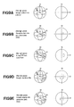
- FIG. 6 shows, in the Poincare-spherical geography, the polarization of light incident at an azimuth of 45 deg. and having passed through various members, in which FIG. 6A shows the polarization of the light having passed through the polarizer 11A in the incident-side polarization plate 10A, FIG. 6B shows the polarization of the light having passed through the protective layer 13A in the incident-side polarization plate 10A, FIG. 6C shows the polarization of the light having passed through the IPS liquid crystal layer 21 in the liquid crystal plate 20, and FIG. 6D shows the polarization of the light having passed through the protective layer 13B in the outgoing-side polarization plate 10B.
- the liquid crystal layer 21 works generally as a ⁇ /2 plate with a predetermined wavelength of green (G) light.
- G green
- the liquid crystal layer 21 functions to reduce the influence of the negative phase difference of the polarization plate-protective layer 13A as will be seen from the Poincare-spherical geography.
- the polarized light having passed through the protective layer 13B in the outgoing-side polarization plate is displaced from the absorption axis of the outgoing-side polarizer 11B when the viewing angle is 45 deg., resulting in light transmission.
- coloring takes place. These are caused mainly by the dependence, upon the wavelength, of the light path length difference ⁇ nd LC of the liquid crystal layer 21.
- a retardation film optimized for the negative phase difference is inserted in a position P1 between the liquid crystal plate 20 and outgoing-side polarization plate 10A or in a position P2 between the outgoing-side polarization plate 10A and liquid crystal layer 20 or in both these positions to reduce the black4evel light leakage at the azimuth of 45 deg.
- a retardation film to cancel the displacement of the polarization axis of the polarizer is required. Also, consideration has to be given to the phase difference of the polarization plate-protective layer.
- FIG. 7 shows the dependence, upon the incident angle, of the displacement of the incident polarization axis and phase difference of the polarization plate-protective layer when the viewing angle is 45 deg.
- the ratio between the displacement of the incident polarization axis and phase change of the polarization plate-protective layers is generally constant with respect to the change in incident angle, which will be described in detail later.
- the liquid crystal layer 21 may be considered as a uniaxial retardation film and the phase difference of the liquid crystal layer 21 be considered as constant in the direction of 45 deg. as having previously been described.
- a retardation film whose delay-phase axis is constant at whatever angle the light is incident and which has a phase difference independent of any incident angle to direct the polarization axis orthogonally to the direction of absorption of the outgoing-side polarizer 11B.
- the refractive index in the direction of thickness is nz
- maximum refractive index in a plane perpendicular to the thickness direction is nx
- refractive index in a direction perpendicular to a direction for the maximum refractive index nx and thickness direction for a refractive index nz is ny
- the delay-phase axis of the retardation film will be directed at an angle of 45 deg. independently of any incident angle. Also, the phase difference is constant independently of any incident angle.
- the plane-directional light path length difference ⁇ nd RF of the biaxial retardation film 30 is adjusted based on the light path length difference ⁇ nd TAC0 of the polarization plane-protective layers 13A and 12B
- FIG. 9 shows, in the Poincare-spherical geography, the polarization of light incident in a direction of 45 deg. and having passed through various members in the liquid crystal display device 100A in FIG. 8, in which FIG. 9A shows the polarization of the light having passed through the polarizer 11A in the incident-side polarization plate 10A, FIG. 9B shows the polarization of the light having passed through the protective layer 13A in the incident-side polarization plate 10A, FIG. 9C shows the polarization of the light having passed through the IPS liquid crystal layer 21 in the liquid crystal plate 20, FIG. 19D shows the polarization of the light having passed through the biaxial retardation film 30, and FIG. 9E shows the polarization of the light having passed through the protective layer 13B in the outgoing-side polarization plate 10B.
- the polarization can be converted into symmetrical points with respect to a plane passing through coordinate axes S2 and S3 by appropriately adjusting the phase difference of the biaxial retardation film 30. Thereafter, the negative phase difference of the protective layer 13B in the outgoing-side polarization plate restores the polarization to the equator of the Poincare sphere and the polarization is made in the direction of the absorption axis of the polarizer 11B in the outgoing-side polarization plate.
- the optimum light path length difference ⁇ nd RF of the biaxial retardation film 30 can be expressed as a function of the light path length difference ⁇ nd TAC0 of the polarization plate-protective layers 13A and 12B as given by the following equation (3):
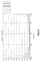
- FIG. 11 shows the relation between the light path length difference ⁇ nd TAC0 of the polarization plate-protective layers 13A and 12B and optimum light path length difference ⁇ nd RF of the biaxial retardation film 30.
- the aforementioned first method of optimizing the retardation film is intended for optimizing the retardation film 30 for an improved black level at a predetermined wavelength in the direction of 45 deg.
- the method of optimizing the retardation film 30 for an improved black level in a wider range of wavelength will be described herebelow.
- the abnormal light refractive index of liquid crystal molecules of the liquid crystal layer 21 is ne
- normal light refractive index is no
- refractive index difference ⁇ n of the liquid crystal layer 21 is (ne - no)
- the light path length difference ⁇ nd LC of the liquid crystal layer 21 is (ne - no) ⁇ d LC .
- the liquid crystal layer 21 functions as a ⁇ /2 plate with a predetermined wavelength.
- the material of the liquid crystal layer 21 shows a wavelength dispersion with the refractive index difference ⁇ n.
- the shorter the wavelength the larger the refractive index difference ⁇ n will be.
- the phase difference is given by 2 ⁇ / ⁇ nd LC , the shorter the wavelength, the larger the phase difference will be. That is, in case the phase difference is set to ⁇ with the wavelength of green (G) light, for example, the phase difference will be larger than ⁇ with the wavelength of blue (B) light and smaller than ⁇ with the wavelength of red (R) light.
- the wavelength dispersion of the retardation film 20 is similar to that of the liquid crystal.
- the light having passed through the protective layer 13A in the incident-side polarization plate is polarized on the northern hemisphere in the Poincare-spherical geography under the conditions in the first optimizing method, as shown in FIG. 12.
- light having passed through the liquid crystal layer 21 and having a wavelength whose phase difference being ⁇ clockwise about the delay-phase axis on the equator is polarized in a position on the southern hemisphere, 180 deg. turned symmetrically from that on the northern hemisphere.
- Light having a shorter wavelength is polarized in a size larger than that at 180 deg.
- light having a longer wavelength is polarized in a size smaller than that at 180 deg.
- FIG. 12A shows the polarization of the light having passed through the polarizer 11A in the incident-side polarization plate 10A
- FIG. 12B shows the polarization of the light having passed through the protective layer 13A in the incident-side polarization plate 10A
- FIG. 12C shows the polarization of the light having passed through the IPS liquid crystal layer 21 in the liquid crystal plate 20
- FIG. 12D shows the polarization of the light having passed through the biaxial retardation film
- FIG. 12E shows the polarization of the light having passed through the protective layer 13B in the outgoing-side polarization plate 10B.
- the polarization of the light having passed through the biaxial retardation film 30 will be discussed. Since the alignment direction of the liquid crystal layer 21 is set to be the same as a direction nx (for the maximum refractive index), the light is also polarized in a position clockwise turned about the coordinate axis S2. Light having a designed wavelength will be polarized in a position symmetrically turned about the S2-S3 plane. Light having a wavelength shorter than that having the designed one will be polarized in a position turned through a larger angle, and light having a wavelength longer than the designed one will be polarized in a position turned through a smaller angle.
- nx for the maximum refractive index
- Light having a wavelength largely different from the designed one will be polarized with a sum of a deviation of the polarization of the light having passed through the liquid crystal layer 21 and a deviation of the polarization of the light having passed through the biaxial retardation film 30, resulting in a larger light leakage.
- the biaxial retardation film 30 is set such that the refractive index will be nx in a direction perpendicular to the alignment direction of the liquid crystal layer 21.
- the optimum light path length difference ⁇ nd RF of the biaxial retardation film 30 is given by the following equation (6):
- FIG. 13A shows the polarization of the light having passed through the polarizer 11A in the incident-side polarization plate 10A
- FIG. 13B shows the polarization of the light having passed through the protective layer 13A in the incident-side polarization plate 10A
- FIG. 13C shows the polarization of the light having passed through the IPS liquid crystal layer 21 in the liquid crystal plate 20
- FIG. 13D shows the polarization of the light having passed through the biaxial retardation film 30
- FIG. 13E shows the polarization of the light having passed through the protective layer 13B in the outgoing-side polarization plate 10B.
- light having the designed wavelength and having passed through the liquid crystal layer 21 is polarized in a position turned by ⁇ .
- light having a wavelength shorter than the designed one is polarized in a position turned by larger than ⁇ while light having a wavelength longer than the designed one is polarized in a position turned by smaller than ⁇ .
- the polarization is made in a position counterclockwise in a direction opposite to the liquid crystal layer 21 because the lead-phase axis of the biaxial retardation film 30 serves as the coordinate axis S2.
- Light having the designed wavelength will be polarized in the same position as in the first optimizing method.
- the deviation of the light having passed through the liquid crystal layer 21 is corrected. Therefore, the compensation can be made in a wide range of wavelength.
- the light path length difference ⁇ nd TAC0 of the polarization plate-protective layers 13A and 12B is large or small, it can be compensated of light having a predetermined wavelength only at a viewing angle in a direction of 45 deg.
- the light path length difference ⁇ nd TAC0 of the polarization plate-protective layers 13A and 12B should desirably be smaller for an improved visibility of light of a wide range of wavelength at a viewing angle in other than 45 deg.
- Many of large LCDs use protective layers of 80 ⁇ m in thickness ( ⁇ nd of 50 nm), and also protective layers of 40 ⁇ m (And of 30 nm) as well in applications in which major consideration is given to the thickness and weight of the LCD display.
- the LCD performance can be improved using polarization plates each protected by thinner protective layers.
- the LCD performance changes depending upon the magnitude and direction of the pretilt angle of the liquid crystal molecules in the liquid crystal layer 21.
- the LCD performance in the first quadrant is generally the same as that in the second quadrant, while the LCD performance in the third quadrant is generally the same as that in the fourth quadrant.
- the pretilt angle should desirably be smaller.
- the light path length difference ⁇ nd LC of the liquid crystal layer 21 has an influence on the black level of light having other wavelength than the designed one.
- the spectral transmittance of light having a longer wavelength can be made relatively higher by setting a shorter designed wavelength, and the chromaticity of the black level can be adjusted by making the spectral transmittance of light having a shorter wavelength relatively lower.
- the "designed wavelength” is a wavelength at which the light path length difference ⁇ nd LC of the liquid crystal layer 21 meets the condition ⁇ /2.
- the second optimizing method enables optical compensation of the polarizers in a wider range of wavelength than by the first optimizing method as having been described in the foregoing.
- either the first or second optimizing method should be selected taking account of which method contributes to the easier production of the retardation film 30 and easier attachment of the retardation film 30 to the polarization plate 10B.
- the light path length difference ⁇ nd RF is larger than with the first optimizing method.
- the retardation film 30 will be difficult to produce or the light path length difference ⁇ nd RF will be uneven.
- the second optimizing method should desirably be used from the viewpoint of production as far as the attachment of the polarization plate 10B and retardation film 30 is concerned.
- the biaxial retardation film 30 can only be produced to have a light path length difference ⁇ nd RF being smaller than a target value, it may be formed from a plurality of retardation films to adjust the light path length difference to the target value.
- the liquid crystal display device 100A was configured to meet the following conditions: Direction of absorption axis of incident-side polarization plate 90 deg. Alignment direction of liquid crystal layer 90 deg. Direction of biaxial retardation film for maximum refractive index nx 90 deg. Direction of absorption axis of outgoing-side polarization plate 0 deg. Designed wavelength 550 nm ⁇ nd LC of liquid crystal layer 275 nm Pretilt angle of liquid crystal layer 2 deg.
- the viewing angle characteristic at a black-display level is as shown in FIG. 14, the black-level spectral transmittance at a viewing angle Pola (elevation angle) of 70 deg. and each of azimuths Azim of 15, 30, 45, 60 and 75 deg. is shown as in FIG. 15, and the black-level spectral transmittance at a viewing angle Pola (elevation angle) of 70 deg. and each of azimuths Azim of 345, 330, 315, 300 and 285 deg. is shown as in FIG. 16.
- the azimuth Azim is a counterclockwise angle based on a viewing angle Pola of 0 deg. from the right side in the drawings.
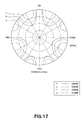
- the liquid crystal display device 100A was configured to meet the following conditions: Direction of absorption axis of incident-side polarization plate 90 deg. Alignment direction of liquid crystal layer 90 deg. Direction of biaxial retardation film for maximum refractive index nx 0 deg. Direction of absorption axis of outgoing-side polarization plate 0 deg. Designed wavelength 550 nm ⁇ nd LC of liquid crystal layer 275 nm Pretilt angle of liquid crystal layer 2 deg.
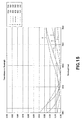
- the viewing angle characteristic at a black-display level is as shown in FIG. 17, the black-level spectral transmittance at a viewing angle Pola (elevation angle) of 70 deg. and each of azimuths Azim of 15, 30, 45, 60 and 75 deg. is shown as in FIG. 18, and the black-level spectral transmittance at a viewing angle Pola (elevation angle) of 70 deg. and each of azimuths Azim of 345, 330, 315, 300 and 285 deg. is shown as in FIG. 19.
- the azimuth Azim is a counterclockwise angle based on a viewing angle Pola of 0 deg. from the right side in the drawings.
- the liquid crystal display device 100A was configured to meet the following conditions: Direction of absorption axis of incident-side polarization plate 90 deg. Alignment direction of liquid crystal layer 90 deg. Direction of biaxial retardation film for maximum refractive index nx 90 deg. Direction of absorption axis of outgoing-side polarization plate 0 deg. Designed wavelength 550 nm ⁇ nd LC of liquid crystal layer 275 nm Pretilt angle of liquid crystal layer 2 deg.
- the viewing angle characteristic at a black-display level is as shown in FIG. 20
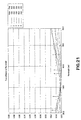
- the black-level spectral transmittance at a viewing angle Pola (elevation angle) of 70 deg. and each of azimuths Azim of 15, 30, 45, 60 and 75 deg. is shown as in FIG. 21
- the black-level spectral transmittance at a viewing angle Pola (elevation angle) of 70 deg. and each of azimuths Azim of 345, 330, 315, 300 and 285 deg. is shown as in FIG. 22.
- the azimuth Azim is a counterclockwise angle based on a viewing angle Pola of 0 deg. from the right side in the drawings.
- the liquid crystal display device 100A was configured to meet the following conditions: Direction of absorption axis of incident-side polarization plate 90 deg. Alignment direction of liquid crystal layer 90 deg. Direction of biaxial retardation film for maximum refractive index nx 0 deg. Direction of absorption axis of outgoing-side polarization plate 0 deg. Designed wavelength 550 nm ⁇ nd LC of liquid crystal layer 275 nm Pretilt angle of liquid crystal layer 2 deg.
- the viewing angle characteristic at a black-display level is as shown in FIG. 20
- the black-level spectral transmittance at a viewing angle Pola (elevation angle) of 70 deg. and each of azimuths Azim of 15, 30, 45, 60 and 75 deg. is shown as in FIG. 24, and the black-level spectral transmittance at a viewing angle Pola (elevation angle) of 70 deg. and each of azimuths Azim of 345, 330, 315, 300 and 285 deg. is shown as in FIG. 25.
- the azimuth Azim is a counterclockwise angle based on a viewing angle Pola of 0 deg. from the right side in the drawings.
- the liquid crystal display device 100A was configured to meet the following conditions: Direction of absorption axis of incident-side polarization plate 90 deg. Alignment direction of liquid crystal layer 90 deg. Direction of biaxial retardation film for maximum refractive index nx 0 deg. Direction of absorption axis of outgoing-side polarization plate 0 deg. Designed wavelength 550 nm ⁇ nd LC of liquid crystal layer 275 nm Pretilt angle of liquid crystal layer 0.5 deg.
- the viewing angle characteristic at a black-display level is as shown in FIG. 26, the black-level spectral transmittance at a viewing angle Pola (elevation angle) of 70 deg. and each of azimuths Azim of 15, 30, 45, 60 and 75 deg. is shown as in FIG. 27, and the black-level spectral transmittance at a viewing angle Pola (elevation angle) of 70 deg. and each of azimuths Azim of 345, 330, 315, 300 and 285 deg. is shown as in FIG. 28.
- the azimuth Azim is a counterclockwise angle based on a viewing angle Pola of 0 deg. from the right side in the drawings.
- the liquid crystal display device 100A was configured to meet the following conditions: Direction of absorption axis of incident-side polarization plate 90 deg. Alignment direction of liquid crystal layer 90 deg. Direction of biaxial retardation film for maximum refractive index nx 0 deg. Direction of absorption axis of outgoing-side polarization plate 0 deg. Designed wavelength 520 nm ⁇ nd LC of liquid crystal layer 260 nm Pretilt angle of liquid crystal layer 0.5 deg.
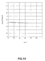
- the viewing angle characteristic at a black-display level is as shown in FIG. 29, the black-level spectral transmittance at a viewing angle Pola (elevation angle) of 70 deg. and each of azimuths Azim of 15, 30, 45, 60 and 75 deg. is shown as in FIG. 30, and the black-level spectral transmittance at a viewing angle Pola (elevation angle) of 70 deg. and each of azimuths Azim of 345, 330, 315, 300 and 285 deg. is shown as in FIG. 31.
- the azimuth Azim is a counterclockwise angle based on a viewing angle Pola of 0 deg. from the right side in the drawings.
- the liquid crystal display device 100A was configured to meet the following conditions: Direction of absorption axis of incident-side polarization plate 90 deg. Alignment direction of liquid crystal layer 90 deg. Direction of biaxial retardation film for maximum refractive index nx 0 deg. Direction of absorption axis of outgoing-side polarization plate 0 deg. Designed wavelength 550 nm ⁇ nd LC of liquid crystal layer 275 nm Pretilt angle of liquid crystal layer 2 deg.
- the viewing angle characteristic at a black-display level is as shown in FIG. 32
- the black-level spectral transmittance at a viewing angle Pola (elevation angle) of 70 deg. and each of azimuths Azim of 15, 30, 45, 60 and 75 deg. is shown as in FIG. 33
- the black-level spectral transmittance at a viewing angle Pola (elevation angle) of 70 deg. and each of azimuths Azim of 345, 330, 315, 300 and 285 deg. is shown as in FIG. 34.
- the azimuth Azim is a counterclockwise angle based on a viewing angle Pola of 0 deg. from the right side in the drawings.
- the liquid crystal display device 100A was configured to meet the following conditions: Direction of absorption axis of incident-side polarization plate 90 deg. Alignment direction of liquid crystal layer 90 deg. Direction of biaxial retardation film for maximum refractive index nx 90 deg. Direction of absorption axis of outgoing-side polarization plate 0 deg. Designed wavelength 550 nm ⁇ nd LC of liquid crystal layer 275 nm Pretilt angle of liquid crystal layer 2 deg.
- the viewing angle characteristic at a black-display level is as shown in FIG. 35
- the black-level spectral transmittance at a viewing angle Pola (elevation angle) of 70 deg. and each of azimuths Azim of 15, 30, 45, 60 and 75 deg. is shown as in FIG. 36
- the black-level spectral transmittance at a viewing angle Pola (elevation angle) of 70 deg. and each of azimuths Azim of 345, 330, 315, 300 and 285 deg. is shown as in FIG. 37.
- the azimuth Azim is a counterclockwise angle based on a viewing angle Pola of 0 deg. from the right side in the drawings.
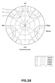
- the liquid crystal display device 100A was configured to meet the following conditions: Direction of absorption axis of incident-side polarization plate 90 deg. Alignment direction of liquid crystal layer 90 deg. Direction of biaxial retardation film for maximum refractive index nx 0 deg. Direction of absorption axis of outgoing-side polarization plate 0 deg. Designed wavelength 550 nm ⁇ nd LC of liquid crystal layer 275 nm Pretilt angle of liquid crystal layer 2 deg.
- the viewing angle characteristic at a black-display level is as shown in FIG. 38
- the black-level spectral transmittance at a viewing angle Pola (elevation angle) of 70 deg. and each of azimuths Azim of 15, 30, 45, 60 and 75 deg. is shown as in FIG. 39
- the black-level spectral transmittance at a viewing angle Pola (elevation angle) of 70 deg. and each of azimuths Azim of 345, 330, 315, 300 and 285 deg. is shown as in FIG. 40.
- the azimuth Azim is a counterclockwise angle based on a viewing angle Pola of 0 deg. from the right side in the drawings.
- the above embodiments can provide the same display. That is, even with the layers of the LCD structure being disposed in an inverted order, the same result can be assured.
- the retardation film is located between the incident-side polarization plate and liquid crystal layer. Also, even with the azimuth of the entire LCD structure turned 90 deg., the same result can be assured.
- the above-mentioned optical compensation can be made in the in-plane switching mode type liquid crystal display device in which the liquid crystal molecules are activated by a field parallel to the substrate as well as in an in-plane switching mode type liquid crystal display device using a ferroelectric liquid crystal whose molecules are activated by a field perpendicular to the substrate.
- the polarization plate can optically be compensated using a retardation film in place of any liquid crystal layer.
- the incident-side polarization plate 10A, retardation film 30, liquid crystal plate 20 and outgoing-side polarization plate 10B may be disposed in this order in a liquid crystal display device 100B as shown in FIG. 41.
- An embodiment 10 of this liquid crystal display device 100B will be described in detail below.
- the liquid crystal display device 100B was configured to meet the following conditions: Direction of absorption axis of incident-side polarization plate 0 deg. Alignment direction of liquid crystal layer 90 deg. Direction of biaxial retardation film for maximum refractive index nx 0 deg. Direction of absorption axis of outgoing-side polarization plate 90 deg. Designed wavelength 550 nm ⁇ nd LC of liquid crystal layer 275 nm Pretilt angle of liquid crystal layer 2 deg.
- the above embodiment 9 may have the entire azimuth thereof turned through 90 deg., which will be described below as an embodiment 11.
- the liquid crystal display device 100A was configured to meet the following conditions: Direction of absorption axis of incident-side polarization plate 0 deg. Alignment direction of liquid crystal layer 0. deg. Direction of biaxial retardation film for maximum refractive index nx 90 deg. Direction of absorption axis of outgoing-side polarization plate 90 deg. Designed wavelength 550 nm ⁇ nd LC of liquid crystal layer 275 nm Pretilt angle of liquid crystal layer 2 deg.
- an incident-side polarization plate 10A, biaxial retardation film 30A, liquid crystal plate 20, biaxial retardation film 30B and outgoing-side polarization plate 10B are disposed in this order in a liquid crystal display device 100C as shown in FIG. 42.
- a liquid crystal display device 100C as shown in FIG. 42.
- more than one combination of the direction, light path length difference and refractive index (nx, ny, nz) of angular direction of the biaxial retardation films 30A and 30B are possible.
- the optimizing method described herebelow is just one of such combinations.
- the light path length difference ⁇ nd RF1 of the biaxial retardation film 30A is set so that the polarization of light having passed through the liquid crystal layer 21 will be equal to that of the light having passed through the protective layer 13A in the incident-side polarization plate 10A.
- the biaxial retardation film 30A is used as a first retardation film to cancel a change in polarized state of the light due to having passed through the liquid crystal layer 21 to restore the polarized state of the light having passed through the protective layer 13A, while the biaxial retardation film 30B is used as a second retardation film acting as a ⁇ /2 plate to change the polarized state through 180 deg., so that the change in polarized state of the light due to having passed through the outgoing-side polarization plate 12B will be canceled by the protective layer 13A in the incident-side polarization plate 10A.
- FIG. 43A shows the polarization of the light having passed through the polarizer 11A in the incident-side polarization plate 10A
- FIG. 43B shows the polarization of the light having passed through the protective layer 13A in the incident-side polarization plate 10A
- FIG. 43C shows the polarization of the light having passed through the retardation film 30A
- FIG. 43D shows the polarization of the light having passed through the IPS liquid crystal layer 21 in the liquid crystal plate 20
- FIG. 43E shows the polarization of the light having passed through the biaxial retardation film 30B
- FIG. 43F shows the polarization of the light having passed through the protective layer 13B in the outgoing-side polarization plate 10B.
- the absorption axis of the incident-side polarization plate 10A is directed at an angle of 90 deg.
- retardation film 30A is directed at an angle of 90 deg. for the maximum refractive index nx
- the liquid crystal plate 20 is aligned at an angle of 90 deg.
- retardation film 30B is directed at an angle of 0 deg. for the maximum refractive index nx
- the absorption axis of the outgoing-side polarization plate 10B is directed at an angle of 0 deg.
- the retardation film 30B may be directed at an angle of 90 deg. but if a plurality of retardation films is directed at the same angle as having been described concerning the second optimizing method, the phase lag when the wavelength of the light is different from the designed one will be larger, resulting in that it will be difficult to suppress the black-level light leakage in a wide range.
- the fourth optimizing method is intended to optimize a biaxial retardation film disposed on either side of the liquid crystal layer.
- the light path length difference ⁇ nd RF1 of the biaxial retardation film 30A in the third optimizing method is given by the following equation (8):
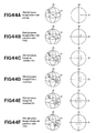
- FIG. 44A shows the polarization of the light having passed through the polarizer 11A in the incident-side polarization plate 10A
- FIG. 44B shows the polarization of the light having passed through the protective layer 13A in the incident-side polarization plate 10A
- FIG. 44C shows the polarization of the light having passed through the retardation film 30A
- FIG. 44D shows the polarization of the light having passed through the IPS liquid crystal layer 21 in the liquid crystal plate 20
- FIG. 44E shows the polarization of the light having passed through the biaxial retardation film 30B
- FIG. 44F shows the polarization of the light having passed through the protective layer 13B in the outgoing-side polarization plate 10B.
- the absorption axis of the incident-side polarization plate 10A is directed at an angle of 90 deg.
- retardation film 30A is directed at an angle of 0 deg. for the maximum refractive index nx
- the liquid crystal layer 21 is aligned at an angle of 90 deg.
- retardation film 30B is directed at an angle of 0 deg. for the maximum refractive index nx
- the absorption axis of the outgoing-side polarization plate 10B is directed at an angle of 0 deg.
- retardation film 30B may be directed at an angle of 90 deg. but the dependence thereof upon the wavelength will be larger.
- compensation can be made of the other retardation film (30A) if the latter is a uniaxial one.
- the light having passed through the protective layer 13B in the outgoing-side polarization plate 10B will be polarized along the absorption axis of the outgoing-side polarization plate 10B irrespectively of the value of the light path length difference ⁇ nd TAC0 of the protective layer 13A in the outgoing-side polarization plate 10A.
- the direction in which the refractive index of the biaxial retardation film is nx is made orthogonal to the absorption axis of the liquid crystal layer.
- the liquid crystal display device 100C was configured to meet the following conditions: Direction of absorption axis of incident-side polarization plate 90 deg. Direction of biaxial retardation film 1 for maximum refractive index nx 90 deg. Alignment direction of liquid crystal layer 90 deg. Direction of biaxial retardation film 2 for maximum refractive index nx 0 deg. Direction of absorption axis of outgoing-side polarization plate 0 deg. Designed wavelength 520 nm ⁇ nd LC of liquid crystal layer 260 nm Pretilt angle of liquid crystal layer 2 deg.
- the viewing angle characteristic at a black-display level is as shown in FIG. 45
- the black-level spectral transmittance at a viewing angle Pola (elevation angle) of 70 deg. and each of azimuths Azim of 15, 30, 45, 60 and 75 deg. is shown as in FIG. 46
- the black-level spectral transmittance at a viewing angle Pola (elevation angle) of 70 deg. and each of azimuths Azim of 345, 330, 315, 300 and 285 deg. is shown as in FIG. 47.
- the azimuth Azim is a counterclockwise angle based on a viewing angle Pola of 0 deg. from the right side in the drawings.
- the liquid crystal display device 100C was configured to meet the following conditions: Direction of absorption axis of incident-side polarization plate 90 deg. Direction of biaxial retardation film 1 for maximum refractive index nx 0 deg. Alignment direction of liquid crystal layer 90 deg. Direction of biaxial retardation film 2 for maximum refractive index nx 0 deg. Direction of absorption axis of outgoing-side polarization plate 0 deg. Designed wavelength 520 nm ⁇ nd LC of liquid crystal layer 260 nm Pretilt angle of liquid crystal layer 0.5 deg.
- the viewing angle characteristic at a black-display level is as shown in FIG. 48
- the black-level spectral transmittance at a viewing angle Pola (elevation angle) of 70 deg. and each of azimuths Azim of 15, 30, 45, 60 and 75 deg. is shown as in FIG. 49
- the black-level spectral transmittance at a viewing angle Pola (elevation angle) of 70 deg. and each of azimuths Azim of 345, 330, 315, 300 and 285 deg. is shown as in FIG. 50.
- the azimuth Azim is a counterclockwise angle based on a viewing angle Pola of 0 deg. from the right side in the drawings.
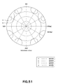
- the liquid crystal display device 100C was configured to meet the following conditions: Direction of absorption axis of incident-side polarization plate 90 deg. Direction of biaxial retardation film 1 for maximum refractive index nx 90 deg. Alignment direction of liquid crystal layer 90 deg. Direction of biaxial retardation film 2 for maximum refractive index nx 0 deg. Direction of absorption axis of outgoing-side polarization plate 0 deg. Designed wavelength 520 nm ⁇ nd LC of liquid crystal layer 260 nm Pretilt angle of liquid crystal layer 0.5 deg.
- the viewing angle characteristic at a black-display level is as shown in FIG. 51
- the black-level spectral transmittance at a viewing angle Pola (elevation angle) of 70 deg. and each of azimuths Azim of 15, 30, 45, 60 and 75 deg. is shown as in FIG. 52
- the black-level spectral transmittance at a viewing angle Pola (elevation angle) of 70 deg. and each of azimuths Azim of 345, 330, 315, 300 and 285 deg. is shown as in FIG. 53.
- the azimuth Azim is a counterclockwise angle based on a viewing angle Pola of 0 deg. from the right side in the drawings.
Landscapes
- Physics & Mathematics (AREA)
- General Physics & Mathematics (AREA)
- Optics & Photonics (AREA)
- Nonlinear Science (AREA)
- Mathematical Physics (AREA)
- Chemical & Material Sciences (AREA)
- Crystallography & Structural Chemistry (AREA)
- Liquid Crystal (AREA)
- Polarising Elements (AREA)
Applications Claiming Priority (3)
| Application Number | Priority Date | Filing Date | Title |
|---|---|---|---|
| JP2003291859 | 2003-08-11 | ||
| JP2003291859 | 2003-08-11 | ||
| PCT/JP2004/011489 WO2005015297A1 (fr) | 2003-08-11 | 2004-08-10 | Ecran a cristaux liquides |
Publications (2)
| Publication Number | Publication Date |
|---|---|
| EP1586939A1 true EP1586939A1 (fr) | 2005-10-19 |
| EP1586939A4 EP1586939A4 (fr) | 2008-02-20 |
Family
ID=34131679
Family Applications (1)
| Application Number | Title | Priority Date | Filing Date |
|---|---|---|---|
| EP04771476A Withdrawn EP1586939A4 (fr) | 2003-08-11 | 2004-08-10 | Ecran a cristaux liquides |
Country Status (7)
| Country | Link |
|---|---|
| US (1) | US7532283B2 (fr) |
| EP (1) | EP1586939A4 (fr) |
| JP (1) | JP4419959B2 (fr) |
| KR (1) | KR101096310B1 (fr) |
| CN (1) | CN100456107C (fr) |
| TW (1) | TWI242083B (fr) |
| WO (1) | WO2005015297A1 (fr) |
Cited By (1)
| Publication number | Priority date | Publication date | Assignee | Title |
|---|---|---|---|---|
| WO2005050302A1 (fr) | 2003-11-21 | 2005-06-02 | Lg Chem, Ltd. | Affichage a cristaux liquides de commutation dans le plan comprenant un film de compensation pour un champ angulaire de visualisation faisant appel a un film de retard biaxial positif |
Families Citing this family (23)
| Publication number | Priority date | Publication date | Assignee | Title |
|---|---|---|---|---|
| JP4536489B2 (ja) * | 2004-11-15 | 2010-09-01 | 株式会社 日立ディスプレイズ | 光学素子及びそれを用いた表示装置 |
| JP4536543B2 (ja) * | 2005-02-08 | 2010-09-01 | 株式会社 日立ディスプレイズ | 液晶表示装置 |
| JP4944387B2 (ja) * | 2005-04-13 | 2012-05-30 | 帝人株式会社 | 液晶表示装置およびそれに用いられる光学フィルム |
| JP4944392B2 (ja) * | 2005-05-16 | 2012-05-30 | 帝人株式会社 | 液晶表示装置およびそれに用いられる光学フィルム |
| JP5311605B2 (ja) | 2005-06-30 | 2013-10-09 | 日東電工株式会社 | 液晶パネルおよび液晶表示装置 |
| CN100454107C (zh) * | 2005-06-30 | 2009-01-21 | 日东电工株式会社 | 液晶面板和液晶显示装置 |
| JP2007057665A (ja) * | 2005-08-23 | 2007-03-08 | Fujifilm Corp | 光学フィルム、画像表示装置、液晶表示装置 |
| JP2007193272A (ja) * | 2006-01-23 | 2007-08-02 | Toshiba Matsushita Display Technology Co Ltd | 液晶表示装置 |
| KR101386565B1 (ko) * | 2006-06-30 | 2014-04-18 | 엘지디스플레이 주식회사 | 액정표시장치 및 그 제조방법 |
| KR101197162B1 (ko) * | 2008-08-27 | 2012-11-09 | 주식회사 엘지화학 | 면상 스위칭 모드 액정 표시 장치 |
| KR101260841B1 (ko) * | 2008-12-23 | 2013-05-06 | 엘지디스플레이 주식회사 | 횡전계방식 액정표시장치 |
| KR101291806B1 (ko) * | 2010-12-10 | 2013-07-31 | 엘지디스플레이 주식회사 | 입체영상 표시장치 |
| WO2013022245A2 (fr) * | 2011-08-05 | 2013-02-14 | 주식회사 엘지화학 | Film optique |
| KR101544249B1 (ko) * | 2011-08-05 | 2015-08-13 | 주식회사 엘지화학 | 광학 필름 |
| CN102854660B (zh) * | 2012-09-24 | 2015-02-11 | 深圳市华星光电技术有限公司 | 一种使用光学补偿膜减弱va液晶显示器暗态漏光的方法 |
| CN102981311B (zh) * | 2012-12-07 | 2016-03-30 | 京东方科技集团股份有限公司 | 显示面板及显示装置 |
| KR101789896B1 (ko) * | 2013-02-01 | 2017-10-25 | 미쯔이가가꾸가부시끼가이샤 | 표시 장치 및 적층 광학 필름 |
| CN105700217A (zh) * | 2014-11-26 | 2016-06-22 | 联想(北京)有限公司 | 一种偏光片、液晶显示屏和电子设备 |
| KR102274545B1 (ko) | 2014-12-01 | 2021-07-06 | 삼성전자주식회사 | 광학 필름용 조성물, 필름 및 표시 장치 |
| CN104950375A (zh) * | 2015-06-19 | 2015-09-30 | 南京中电熊猫液晶显示科技有限公司 | 一种液晶显示器用的上偏光板、液晶显示器 |
| CN107367849B (zh) * | 2017-08-31 | 2019-10-18 | 深圳市华星光电技术有限公司 | 显示装置及偏光太阳眼镜 |
| KR102444973B1 (ko) * | 2019-06-19 | 2022-09-19 | 삼성에스디아이 주식회사 | 편광판 및 이를 포함하는 광학표시장치 |
| KR102859724B1 (ko) * | 2020-03-18 | 2025-09-15 | 삼성디스플레이 주식회사 | 표시 장치 |
Family Cites Families (11)
| Publication number | Priority date | Publication date | Assignee | Title |
|---|---|---|---|---|
| JP3299190B2 (ja) | 1998-07-15 | 2002-07-08 | インターナショナル・ビジネス・マシーンズ・コーポレーション | 液晶表示装置 |
| JP2002148661A (ja) * | 2000-08-31 | 2002-05-22 | Sharp Corp | 液晶表示装置 |
| JP2002072215A (ja) * | 2000-08-31 | 2002-03-12 | Sharp Corp | 液晶表示装置 |
| JP4276778B2 (ja) * | 2000-12-25 | 2009-06-10 | 富士フイルム株式会社 | 光学補償シートの製造方法 |
| JP2002258041A (ja) * | 2001-03-01 | 2002-09-11 | Nitto Denko Corp | 光学補償偏光板及び液晶表示装置 |
| JP3942436B2 (ja) * | 2001-07-19 | 2007-07-11 | 日東電工株式会社 | 偏光板およびその製造方法、偏光板用保護フィルム、偏光板を用いた光学フイルムならびに画像表示装置 |
| JP3863446B2 (ja) | 2002-03-08 | 2006-12-27 | シャープ株式会社 | 液晶表示装置 |
| JP4145535B2 (ja) * | 2002-03-08 | 2008-09-03 | シャープ株式会社 | 液晶表示装置のリターデーション設定方法 |
| JP3993000B2 (ja) * | 2002-03-08 | 2007-10-17 | シャープ株式会社 | 液晶表示装置のリターデーションの設定方法 |
| KR100822247B1 (ko) * | 2002-04-01 | 2008-04-16 | 닛토덴코 가부시키가이샤 | 광학 필름 및 화상 표시 시스템 |
| JP3687854B2 (ja) * | 2002-10-15 | 2005-08-24 | 日東電工株式会社 | 光学フィルムおよび液晶表示装置 |
-
2004
- 2004-08-09 TW TW093123819A patent/TWI242083B/zh not_active IP Right Cessation
- 2004-08-10 EP EP04771476A patent/EP1586939A4/fr not_active Withdrawn
- 2004-08-10 US US10/530,828 patent/US7532283B2/en not_active Expired - Fee Related
- 2004-08-10 WO PCT/JP2004/011489 patent/WO2005015297A1/fr not_active Ceased
- 2004-08-10 JP JP2005512995A patent/JP4419959B2/ja not_active Expired - Fee Related
- 2004-08-10 CN CNB2004800015181A patent/CN100456107C/zh not_active Expired - Fee Related
- 2004-08-10 KR KR1020057006244A patent/KR101096310B1/ko not_active Expired - Fee Related
Non-Patent Citations (3)
| Title |
|---|
| ANDERSON J E ET AL: "Methods and concerns of compensating in-plane switching liquid crystal displays" JAPANESE JOURNAL OF APPLIED PHYSICS, JAPAN SOCIETY OF APPLIED PHYSICS, TOKYO, JP, vol. 39, no. 11, November 2000 (2000-11), pages 6388-6392, XP002288101 ISSN: 0021-4922 * |
| SAITOH Y ET AL: "OPTIMUM FILM COMPENSATION OF VIEWING ANGLE OF CONTRAST IN IN-PLANE-SWITCHING-MODE LIQUID CRYSTAL DISPLAY" JAPANESE JOURNAL OF APPLIED PHYSICS, JAPAN SOCIETY OF APPLIED PHYSICS, TOKYO, JP, vol. 37, no. 9A, September 1998 (1998-09), pages 4822-4828, XP000986685 ISSN: 0021-4922 * |
| See also references of WO2005015297A1 * |
Cited By (4)
| Publication number | Priority date | Publication date | Assignee | Title |
|---|---|---|---|---|
| WO2005050302A1 (fr) | 2003-11-21 | 2005-06-02 | Lg Chem, Ltd. | Affichage a cristaux liquides de commutation dans le plan comprenant un film de compensation pour un champ angulaire de visualisation faisant appel a un film de retard biaxial positif |
| EP1685441A4 (fr) * | 2003-11-21 | 2008-02-27 | Lg Chemical Ltd | Affichage a cristaux liquides de commutation dans le plan comprenant un film de compensation pour un champ angulaire de visualisation faisant appel a un film de retard biaxial positif |
| US7446838B2 (en) | 2003-11-21 | 2008-11-04 | Lg Chem Ltd. | In-plane switching liquid crystal display comprising compensation film for angular field of view using positive biaxial retardation film |
| US7671950B2 (en) | 2003-11-21 | 2010-03-02 | Lg Chem. Ltd. | In-plane switching liquid crystal display comprising compensation film for angular field of view using positive biaxial retardation film |
Also Published As
| Publication number | Publication date |
|---|---|
| TW200530638A (en) | 2005-09-16 |
| JP4419959B2 (ja) | 2010-02-24 |
| WO2005015297A1 (fr) | 2005-02-17 |
| TWI242083B (en) | 2005-10-21 |
| US7532283B2 (en) | 2009-05-12 |
| JPWO2005015297A1 (ja) | 2006-10-05 |
| CN100456107C (zh) | 2009-01-28 |
| KR20060059855A (ko) | 2006-06-02 |
| EP1586939A4 (fr) | 2008-02-20 |
| CN1717615A (zh) | 2006-01-04 |
| KR101096310B1 (ko) | 2011-12-20 |
| US20060098146A1 (en) | 2006-05-11 |
Similar Documents
| Publication | Publication Date | Title |
|---|---|---|
| US7532283B2 (en) | Liquid crystal display | |
| US7292299B2 (en) | Liquid crystal display apparatus | |
| JP4002433B2 (ja) | アクティブマトリクス型液晶表示装置 | |
| EP1767966B1 (fr) | Film à différence de phase, film à polarisation, afficheur à cristaux liquides, et méthode pour la conception du film à différence de phase | |
| EP2487536B1 (fr) | Dispositif d'affichage à cristaux liquides | |
| EP2259131B1 (fr) | Dispositif d'affichage à cristaux liquides | |
| US8237899B2 (en) | Liquid crystal display device | |
| US8077277B2 (en) | Liquid crystal display device comprising a first optical compensating member disposed without a birefringent medium sandwiched between the liquid crystal layer and the first optical compensating member | |
| US8149354B2 (en) | Liquid crystal display device | |
| US7719647B2 (en) | Liquid crystal display apparatus | |
| US20120257147A1 (en) | Liquid crystal display panel and liquid crystal display device | |
| US20110304801A1 (en) | Liquid crystal display panel | |
| US7652737B2 (en) | LCD device having an improved viewing angle characteristic | |
| KR100762034B1 (ko) | Ocb 모드 액정표시장치 | |
| KR100763689B1 (ko) | 액정 표시 장치 | |
| WO2005052678A1 (fr) | Unite d'affichage a cristaux liquides | |
| KR101192786B1 (ko) | 액정표시장치 | |
| KR100789681B1 (ko) | 향상된 시야각 특성을 가지는 lcd 장치 | |
| JP2005250032A (ja) | 液晶表示装置の製造方法 |
Legal Events
| Date | Code | Title | Description |
|---|---|---|---|
| PUAI | Public reference made under article 153(3) epc to a published international application that has entered the european phase |
Free format text: ORIGINAL CODE: 0009012 |
|
| 17P | Request for examination filed |
Effective date: 20050411 |
|
| AK | Designated contracting states |
Kind code of ref document: A1 Designated state(s): AT BE BG CH CY CZ DE DK EE ES FI FR GB GR HU IE IT LI LU MC NL PL PT RO SE SI SK TR |
|
| AX | Request for extension of the european patent |
Extension state: AL HR LT LV MK |
|
| DAX | Request for extension of the european patent (deleted) | ||
| RBV | Designated contracting states (corrected) |
Designated state(s): DE FR GB |
|
| A4 | Supplementary search report drawn up and despatched |
Effective date: 20080121 |
|
| 17Q | First examination report despatched |
Effective date: 20130103 |
|
| STAA | Information on the status of an ep patent application or granted ep patent |
Free format text: STATUS: THE APPLICATION IS DEEMED TO BE WITHDRAWN |
|
| 18D | Application deemed to be withdrawn |
Effective date: 20130301 |