EP1587066A2 - Circuit d'attaque d'écriture avec circuit élévateur de tension et interconnexion d'une impédance adaptée - Google Patents
Circuit d'attaque d'écriture avec circuit élévateur de tension et interconnexion d'une impédance adaptée Download PDFInfo
- Publication number
- EP1587066A2 EP1587066A2 EP05008158A EP05008158A EP1587066A2 EP 1587066 A2 EP1587066 A2 EP 1587066A2 EP 05008158 A EP05008158 A EP 05008158A EP 05008158 A EP05008158 A EP 05008158A EP 1587066 A2 EP1587066 A2 EP 1587066A2
- Authority
- EP
- European Patent Office
- Prior art keywords
- write
- circuit
- current
- write driver
- voltage
- Prior art date
- Legal status (The legal status is an assumption and is not a legal conclusion. Google has not performed a legal analysis and makes no representation as to the accuracy of the status listed.)
- Granted
Links
Images






Classifications
-
- G—PHYSICS
- G11—INFORMATION STORAGE
- G11B—INFORMATION STORAGE BASED ON RELATIVE MOVEMENT BETWEEN RECORD CARRIER AND TRANSDUCER
- G11B5/00—Recording by magnetisation or demagnetisation of a record carrier; Reproducing by magnetic means; Record carriers therefor
- G11B5/02—Recording, reproducing, or erasing methods; Read, write or erase circuits therefor
-
- G—PHYSICS
- G11—INFORMATION STORAGE
- G11B—INFORMATION STORAGE BASED ON RELATIVE MOVEMENT BETWEEN RECORD CARRIER AND TRANSDUCER
- G11B5/00—Recording by magnetisation or demagnetisation of a record carrier; Reproducing by magnetic means; Record carriers therefor
- G11B5/02—Recording, reproducing, or erasing methods; Read, write or erase circuits therefor
- G11B5/022—H-Bridge head driver circuit, the "H" configuration allowing to inverse the current direction in the head
-
- G—PHYSICS
- G11—INFORMATION STORAGE
- G11B—INFORMATION STORAGE BASED ON RELATIVE MOVEMENT BETWEEN RECORD CARRIER AND TRANSDUCER
- G11B5/00—Recording by magnetisation or demagnetisation of a record carrier; Reproducing by magnetic means; Record carriers therefor
- G11B2005/0002—Special dispositions or recording techniques
- G11B2005/0005—Arrangements, methods or circuits
- G11B2005/001—Controlling recording characteristics of record carriers or transducing characteristics of transducers by means not being part of their structure
- G11B2005/0013—Controlling recording characteristics of record carriers or transducing characteristics of transducers by means not being part of their structure of transducers, e.g. linearisation, equalisation
- G11B2005/0016—Controlling recording characteristics of record carriers or transducing characteristics of transducers by means not being part of their structure of transducers, e.g. linearisation, equalisation of magnetoresistive transducers
- G11B2005/0018—Controlling recording characteristics of record carriers or transducing characteristics of transducers by means not being part of their structure of transducers, e.g. linearisation, equalisation of magnetoresistive transducers by current biasing control or regulation
-
- H—ELECTRICITY
- H02—GENERATION; CONVERSION OR DISTRIBUTION OF ELECTRIC POWER
- H02M—APPARATUS FOR CONVERSION BETWEEN AC AND AC, BETWEEN AC AND DC, OR BETWEEN DC AND DC, AND FOR USE WITH MAINS OR SIMILAR POWER SUPPLY SYSTEMS; CONVERSION OF DC OR AC INPUT POWER INTO SURGE OUTPUT POWER; CONTROL OR REGULATION THEREOF
- H02M3/00—Conversion of DC power input into DC power output
- H02M3/02—Conversion of DC power input into DC power output without intermediate conversion into AC
- H02M3/04—Conversion of DC power input into DC power output without intermediate conversion into AC by static converters
- H02M3/06—Conversion of DC power input into DC power output without intermediate conversion into AC by static converters using resistors or capacitors, e.g. potential divider
- H02M3/07—Conversion of DC power input into DC power output without intermediate conversion into AC by static converters using resistors or capacitors, e.g. potential divider using capacitors charged and discharged alternately by semiconductor devices with control electrode, e.g. charge pumps
Definitions
- the present invention relates, in general, to hard disk drive (HDD) systems and magneto resistive data storage devices and systems, and, more particularly, to a write driver with a circuit, and associated method, for HDD applications capable of switching a current into a write head, such as a low impedance head, connected to the write driver through a transmission line or interconnect.
- the write driver circuit includes a boosting device or circuit to increase the output voltage launched into the transmission line while maintaining impedance matching between the write driver and the characteristic impedance of the transmission line.
- the magnetic regions are created by passing current through a coil of a magnetic write head.
- Binary data can be encoded by switching the polarity of the current through a coil in the write head.
- the current in the write head coil is provided by a circuit in a write driver that is connected to the coil through a flexible transmission interconnect.
- the data rate i.e., the rate at which bits can be written onto the media
- a conventional write driver circuit comprises an H-bridge configuration using four switches.
- an H-bridge circuit one leg of the bridge is always trying to drive current into the inductive load.
- the H-bridge is always coupling the power supply voltage onto one of the inductor nodes and ground to the other inductor node by appropriately activating the bridge switches.
- the impedance matching circuit includes a resistor having a resistance substantially equal to the odd characteristic impedance of the interconnect to the write head.
- the impedance matching circuit may also include means for generating a voltage pulse to the resistor, with the pulse having an amplitude equal to the output voltage at the output node of the write driver circuit such that the pulsed current from the driver circuit does not flow through the resistor of the impedance matching circuit.
- the write driver also includes a circuit for providing a boosting technique to increase the output voltage launched into the transmission line which enables the write driver to more effectively produce a current pulse for the duration of an overshoot, OSDUR, of a write assembly of the HDD system and with a desired amplitude, i.e., IOS/2, at the output node, HWX (and, typically, HWY), of the write driver.
- a circuit for providing a boosting technique to increase the output voltage launched into the transmission line which enables the write driver to more effectively produce a current pulse for the duration of an overshoot, OSDUR, of a write assembly of the HDD system and with a desired amplitude, i.e., IOS/2, at the output node, HWX (and, typically, HWY), of the write driver.
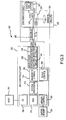
- the data that is exchanged through disk controller 303 is typically buffered in buffer memory 304 that is accessible via memory controller 309 and subsequently transmitted to disk assembly 320 or host 301.
- Buffer memory 304 is used to overcome differences between the speed at which host 301 operates as compared to the speed at which disk assembly 320 operates.
- a cache memory may be implemented by appropriate changes (e.g., tag management, hit/miss detection, and the like) to memory controller 309.
- Servo control 308 regulates the spin speed of spindle motor 324 in response to commands from system processor 313.
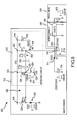
- the write driver 510 is shown to includes a pull-up circuit and described below but, of course, the exemplary pull-up circuit can be utilized by those skilled in the art to obtain a similar pull-down circuit making use of complementary devices as is shown the write assembly 600 of Figure 6 (e.g., PMOS replaced with NMOS transistors and vice versa).
- the write driver 510 includes a boosting circuit 512 linked to a current mirror 522 including transistors 528, 530 fed by reference current generator 520.
- the boosting circuit 512 is also connected to the driver output node 516, which in turn is linked to an impedance matching circuit comprising voltage generator 556 and output resistor 514.
- the resistor 514 is selected to have a resistance, R1, equal to the odd characteristic impedance, Z ODD , of the interconnect line 564.
- the transistor 530 in the boosting circuit 512 acts like a pulsed current generator.
- the amplitude, IOS/2, of the pulsed current generated by the transistor 530 is set by the reference current generator 520 and by the ratio (M1:M17) of the current mirror 522, which may be set to one for simplicity.
- the duration, OSDUR, of the generated current pulse sets the overshoot duration of the load current, IL, at the write head 570.
- OSDUR the current generated by the transistor 530 flows through the capacitor 538, the transistor 544, and the transmission line 564 of the interconnect 560 to the head or load 570 (shown as a short for simplicity).
- the reference or bias voltage generator 548 provides a bias voltage, VBIAS, so that the transistor 544 is at or near the limit of conduction before the overshoot transition occurs avoiding releasing or creating further dynamics at capacitor nodes 536, 540 and also increasing the switching speed since the parasitics are pre-charged at capacitor node 540.
- the output voltage, V HWX swings from 0 Volts to Z ODD • IOS/2 Volts for a period equal to 2T D , where T D is the propagation delay of the interconnect 560.
- the output voltage, V HWX eventually forces transistor 544 in triode for high output current amplitude, IOS/2, settings.
- the output impedance of the overshoot branch nevertheless remains high compared to the odd characteristic impedance, Z ODD , of the interconnect 560 because transistor 530 is still in saturation.
- Diode 550 eventually enters reverse bias allowing capacitor node 540 and output voltage, V HWX , at driver output node 516 to swing above the supply voltage, VCC, up to the limit given in Equation 1.
- switch 534 closes so that the capacitor 538 (through switch 534) and diode 550 can be re-charged to a voltage equal to twice the supply voltage less the voltage of the diode 550 (i.e., 2VCC - V DIODE ).
- the capacitor 538 is then ready for the next transition of the write assembly 500.
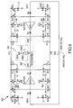
- Figure 6 illustrates a write assembly 600 implementing the write driver techniques of Figure 5 to provide a fully differential circuital implementation of a write driver with a pull-up circuit and a pull-down circuit for selectively driving pulsed current through an interconnect 620 and a write head 630.
- Each of the two symmetrical sides of the write circuit in assembly 600 comprise two of the basic cells or circuits described earlier, such as write driver 510 in Figure 5, to implement the pull-up and pull-down boosted overshoot transient.
- the pull-down overshoot circuit is built making use of complimentary devices with respect to the pull-up overshoot circuit, e.g., with PMOS transistors replaced with NMOS transistors and vice versa.
- boosting circuits and write drivers including such boosting circuits understood with reference to the devices of Figures 3-5, it may be helpful to discuss the components and circuitry of the write driver circuit of assembly 600 with respect to its operation.
- Buffers X and Y in one embodiment are designed to have unity gain and low output impedance and high input impedance compared to the odd characteristic impedance, Z ODD , of the interconnect 620.
- Buffer X, transistor M15, and resistor R3 generate at the output of Buffer X a voltage equal to the output voltage, V HWX .
- Buffer Y, transistor M14, and resistor R4 generate at the output of Buffer Y a voltage equal to the output voltage, V HWY .
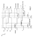
- FIG. 7 illustrates a time diagram 700 for the write driver of the write assembly 600 of Figure 6.
- the duration of the current pulse generated by I1-I4 (which sets the duration, OSDUR, of the overshoot in the head current) is set longer than 2T D , where T D is the electrical length of the interconnect 620.
- the main reflection generated at the head side at a time T D seconds after the beginning of the transition is completely absorbed by the matched write driver at a time of 2T D seconds, and no other reflections propagate after 2T D seconds with the result of producing a clean head current step response.
- the overshoot duration, OSDUR can be set to any value from zero seconds to BITDUR seconds.
- Figure 8 illustrates in a simplified manner a write driver 810 taught by U.S. Patent Application published May 15, 2003 entitled “Write Head Driver Circuit and Method for Writing to a Memory Disk” to Venca et al., Publication No. US 2003/0090828 A1, Serial No. 09/991,557.
- the write driver 810 is illustrated in a manner that allows ready comparison with the write driver 510 of the present invention shown in Figure 5.
- the write driver 810 is used to provide an output voltage and pulsed current on driver output node 840 which is connected to interconnect 860 to provide current, IOS, to load or head 870.
- the write driver 810 includes internal resistor 842 with resistance R1 set to Z ODD to control reflection.
- Driver 810 applies a supply voltage, VCC, at nodes 812, 814, 834 to supply current mirror 820 (and transistors 822, 824) and transistor 838.
- a reference current source 816 is connected to the current mirror 820, and the current mirror is connected to an input node 850 of a buffer 846 having unity gain.
- An additional resistor 856 is provided in a branch off of buffer input node 850 with a resistance R3 set based on a scaling factor, K, relative to the odd characteristic impedance, Z ODD , of the interconnect 860.
- the transistor 838 acts like a pulsed current generator generating a pulse of amplitude IOS/2 and setting the load current overshoot amplitude at IOS.
- the transistor 530 acts similarly even when the overshoot current IOS/2 flows additionally through capacitor 538 and additional transistor 544.
- the output voltage, V HWX produced by driver circuit 810 and produced by driver circuit 510 with boost circuit 512 both show a pulse behavior of a duration, 2T D , and an amplitude equal to Z ODD •IOS/2 as long as the output impedance is maintained of the write driver is maintained equal to the odd character impedance, Z ODD , of the interconnect 560, 860.
- the prior art circuit 810 is not configured to maintain the desired output resistance.
- the transistor 838 of the circuit 810 enters triode condition.
- the overshoot branch then presents a low output impedance that shunts the internal resistor 842 and reduces the total output impedance of the driver 810 to a lower value than the odd characteristic impedance, Z ODD , of the interconnect 860. This results in the undesirable consequence of mismatched impedance between the driver 810 and the interconnect 860 or the output resistance of the driver 810 is "sub-matching" the characteristic impedance of the interconnect 860.
- write driver 810 An important effect of this sub-matching condition in write driver 810 is a reduced output dynamic (or smaller voltage swing). Consequently, the write driver 810 also has a reduced peak current driving capability during these operating periods when compared with the write driver 510 that implements the boosting circuit 512. More particularly, the increased dynamic given to capacitor node 536 of the present invention allows the transistor 530 that acts as a pulsed current generator to work in saturation for an output voltage swing (i.e., a value up to or approaching the value given by Equation 1) exceeding the limit (i.e., VCC - VOV M1 ) experienced by the write driver circuit 810. As can be appreciated, the larger output voltage swing achieved by the write driver 510 significantly improves the peak current performance for the write driver 510 when compared to other embodiments of write drivers, such as write driver 810.
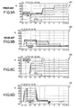
- Figures 9A-9D illustrate graphically a qualitative comparison for a given load.
- Graphs 910, 920, 930, and 940 illustrate the values of load currents and output voltages over time produced by the circuits 510 and 810, with graphs 910 and 920 providing data for the circuit 810 and graphs 930 and 940 providing data for the circuit 510 of the present invention. All the curves are normalized in percentage to the maximum value obtained by the present invention, with the effect of the saturation of the overshoot current branch in circuit 810 being visible at high current overshoot settings.
- Figure 10A illustrates the boosting techniques of the present invention in a write driver circuit 1000
- Figure 10B illustrates a circuit 1050 exemplary of the teaching of U.S. Patent No. 6,512,645 entitled "Circuit and Method for Writing to a Memory Disk with a Boosted Voltage" issued January 28, 2003 to Patti et al.
- the two circuits 1000, 1050 are represented in similar, simplified form to facilitate a clearer understanding of the differences between the two circuits.
- Circuit 1050 is a basic bootstrap circuit configured in an attempt of providing boosting to enhance the output voltage dynamic in a write driver (not shown), and in the following discussion, only pull-down techniques are compared as pull-up boosting circuitry is not described fully in the Patti et al. patent.
- a major difference between the circuits 1000, 1050 is the way in which node A is driven.
- circuit 1050 low impedance voltage drive is used while in the circuit 1000 high impedance current drive is utilized.
- the voltage integration occurs at node B in circuit 1050 but at node A in the circuit 1000 according to the present invention.
- the gate of transistor 1078 in circuit 1050 is kept at a fixed potential during operation of the circuit 1050, the related voltage, V gs , of the circuit 1050 decreases during the overshoot transient due to the integration effect. As a result, the overshoot current is undesirably decreased accordingly.
- the circuit 1050 will show a sub-matching condition (as discussed with reference to driver 810 of Figure 8) during the overshoot. This is because the circuit 1050 has low impedance at node A.
- the circuit 1000 of the present invention always provides impedance matching because the circuit 1000 shows high impedance at node A avoiding in this manner the propagation of reflected waves through the interconnect connected at output node HWX.
- the invention is useful for providing a write driver circuit for HDD applications that is capable of switching a current into a low impedance head connected to the driver through a transmission line.
- the boosting circuits described with regard to these figures provide a useful technique to increase the output voltage launched into the line, which may include impedance matching with the characteristic impedance of the interconnect line.
- the following discussion provides an altemative boosting technique that represent an enhancement or improvement of the output voltage that can be launched to the head through the interconnect while also providing less power consumption when compared with the boosting circuits and write drivers of Figures 4-10.
- the output voltage dynamic is improved over the circuits of Figures 4-6 since the input node 1122 can be pre-charged as low as VEE through the transistor or current source 1141 before the positive pulse is launched and/or can be charged as high as VCC through the transistor or current source 1140 before the negative pulse is launched. If the capacitor 1120 has a large enough capacitance the voltage integration at the input node 1122 can be slow enough to avoid or control the saturation of the current generator 1140 (during positive pulse) and current generator 1141 (during negative pulse) for the entire overshoot duration OSDUR.
- Transistor 1150 or transistor 1152 will eventually enter triode condition during the overshoot transition without affecting the output impedance of the circuit 1100 since it is in series with the high output impedance of the current generators 1140 and 1141.
- VCM (VCC+VEE)/2)
- Output Dynamic Range 2*VCC - VOV M1, M3 before M1 or M3 (or sources 1140, 1141) will enter triode condition and lower the output impedance of the circuit 1100.
- M1 and M3 are transistors in current mirror configuration
- the ohmic drop on transistors 1150, 1152 is negligible.
- Output Dynamic Range 2*VCC - VOV M1,M3 - (IOS*OSDUR)/(2*C1)
- FIG. 12 shows one example of a write assembly 1200 with a write driver 1210 linked to a write head or load 1270 via an interconnect 1260 and comprising a boosting device or circuit 1212.
- the boosting device or circuit 1212 is configured as shown in Figure 11 with like numbers being used to identify the various components of the circuit 1212.
- the boosting device or circuit 1212 is useful for improving the dynamic performances of the pull-up and pull-down circuits of the write driver 1210 as well as the efficiency of the whole write driver 1210 and write assembly 1200.
- the boosting technique discussed with reference to Figure 11 can be implemented in many different ways with the embodiment of the pull-up and pull-down circuit of write driver 1210 shown being just one example that can be readily modified to practice the boosting concepts taught herein.
- a second voltage reference, V2 generates a voltage pulse with duration equal to OSDUR and amplitude equal to the output voltage of the boosting circuit 1212 at output node 1216 or at node 1110 (or HWX). In this manner, the voltage drop across resistor 1214 (or R1) is made equal to zero, thereby avoiding the current IOS/2 coming from the pull-up branch flowing through internal resistor 1214 (or R1).
- the output voltage at HWX (or 1110, 1216) swings from 0 V to Z ODD *IOS/2 V for a period equal to 2*Td, where Td is the propagation delay of the interconnect 1260 and eventually forces transistor 1150 (or M5) into triode for high IOS/2 amplitude settings. Nevertheless, the output impedance of the overshoot branch remains high compared to Z ODD since transistor 1140 (or M1) is still in saturation.
- Figure 13 illustrates a write assembly 1300 (similar to assembly 600 of Figure 6) implementing the write driver techniques, and especially, the pull-up and pull-down circuits, of Figure 6 to provide a fully differential circuital implementation of a write driver with a boosting circuit 1310 and impedance matching circuit 1340 to selectively drive a pulsed current through an interconnect 1320 and a write head 1330.
- the boosting circuit 1310 is shown to contain two symmetrical sides having two of the boosting circuits 1212 of Figure 12 including the current mirrors 1220, 1222, and the impedance matching circuit 1340 is shown to include symmetrical sides or circuits as is described in more detail in U.S. Patent Application No.
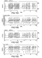
- Figure 14 illustrates a time diagram 1400 for the write driver of the write assembly 1300 provided by boosting circuit 1310 and impedance matching circuit 1340.
- the duration of the current pulse generated by sources 11 and 14 (which sets the duration OSDUR of the overshoot in the head current) is set longer than 2*Td, where Td is the electrical length of the interconnect T1.
- FIG 16 illustrates another embodiment of a write assembly 1600 providing a more detailed circuital implementation of a write driver 1610 according to the invention, starting from the content of the above referred U.S. Patent Application No. 10/824,096 and from the description of the operating of the impedance matching circuit 1340 shown in Figure 13.
- the write assembly 1600 includes a write head 1660 linked to a write driver 1610 with an interconnect 1650.
- the interconnect 1650 is connected to the write head 1660 at node 1622 at which point write head 1610 provides output voltage, HWX, and includes transmission line 1652 with a characteristic odd impedance, Z ODD , and which delays propagated signals by a transmission delay, T D .
- a voltage source to provide a desired input voltage is implemented in the write driver 1610 with a buffer 1630, i.e., Buffer X, transistor Q9 1634, and resistor 1636.
- the buffer 1630 preferably is designed to have unity gain and low output impedance and high input impedance relative to the odd characteristic impedance, Z ODD , of the interconnect 1650. Due to the high input impedance of the buffer 1630, the resistance, R3, of the resistor 1636 can be scaled relative to the impedance of the transmission line 1652, such as K times larger than Z ODD . This also allows the area of transistor Q9 1634 to be much smaller than the transistor Q1 1612, such as K times smaller.
Landscapes
- Digital Magnetic Recording (AREA)
Applications Claiming Priority (4)
| Application Number | Priority Date | Filing Date | Title |
|---|---|---|---|
| US824096 | 2004-04-14 | ||
| US10/824,096 US7375909B2 (en) | 2004-04-14 | 2004-04-14 | Write driver with power optimization and interconnect impedance matching |
| US843823 | 2004-05-12 | ||
| US10/843,823 US7035028B2 (en) | 2004-05-12 | 2004-05-12 | Disk drive write driver with boosting circuit to improve output voltage swing |
Publications (3)
| Publication Number | Publication Date |
|---|---|
| EP1587066A2 true EP1587066A2 (fr) | 2005-10-19 |
| EP1587066A3 EP1587066A3 (fr) | 2005-11-02 |
| EP1587066B1 EP1587066B1 (fr) | 2009-04-08 |
Family
ID=34935159
Family Applications (1)
| Application Number | Title | Priority Date | Filing Date |
|---|---|---|---|
| EP05008158A Expired - Lifetime EP1587066B1 (fr) | 2004-04-14 | 2005-04-14 | Circuit d'attaque d'écriture avec circuit élévateur de tension et interconnexion d'une impédance adaptée |
Country Status (3)
| Country | Link |
|---|---|
| US (1) | US7365928B2 (fr) |
| EP (1) | EP1587066B1 (fr) |
| DE (1) | DE602005013715D1 (fr) |
Families Citing this family (11)
| Publication number | Priority date | Publication date | Assignee | Title |
|---|---|---|---|---|
| ATE439668T1 (de) * | 2004-10-28 | 2009-08-15 | Agere Systems Inc | Verfahren und vorrichtungen zur steuerung des schreibtreiberstroms |
| US7701654B2 (en) * | 2005-09-23 | 2010-04-20 | Agere Systems Inc. | Apparatus and method for controlling common mode voltage of a disk drive write head |
| US7746591B2 (en) * | 2007-12-14 | 2010-06-29 | Texas Instruments Incorporated | Methods and apparatus to provide dynamically-biased write drivers for hard disk drive (HDD) application |
| US7933090B1 (en) * | 2009-01-14 | 2011-04-26 | Western Digital Technologies, Inc. | Disk drive establishing write current limits prior to optimizing the write current for a plurality of tracks |
| US20110116193A1 (en) * | 2009-11-16 | 2011-05-19 | Seagate Technology Llc | Magnetic head with integrated write driver |
| US8424418B1 (en) | 2010-09-30 | 2013-04-23 | Western Digital Technologies, Inc. | Systems and methods for coupling screwdrivers to screw finders |
| US8792197B1 (en) | 2013-09-20 | 2014-07-29 | Lsi Corporation | Storage device with driver controller providing pattern-dependent write functionality |
| KR20160016386A (ko) * | 2014-08-05 | 2016-02-15 | 에스케이하이닉스 주식회사 | 라이트 드라이버, 이를 포함하는 저항변화 메모리 장치 및 동작 방법 |
| US9093097B1 (en) * | 2015-02-06 | 2015-07-28 | Seagate Technology Llc | Ammonite servo reference pattern writing for heat-assisted magnetic recording |
| US9823306B2 (en) * | 2016-02-11 | 2017-11-21 | Texas Instruments Incorporated | Measuring internal signals of an integrated circuit |
| US12475926B1 (en) | 2024-11-01 | 2025-11-18 | Avago Technologies International Sales Pte. Limited | Switchable inductor for boost or matching optimization |
Family Cites Families (33)
| Publication number | Priority date | Publication date | Assignee | Title |
|---|---|---|---|---|
| DE69422164T2 (de) | 1994-05-31 | 2000-04-20 | Stmicroelectronics S.R.L. A | Kapazitive Ladungspumpe, Bicmos Schaltung für niedrige Versorgungsspannung |
| EP0737643B1 (fr) * | 1995-04-14 | 2000-09-13 | STMicroelectronics S.r.l. | Circuit générateur élevateur de tension pour fournir un niveau de tension sensiblement constant |
| US5612828A (en) * | 1995-09-11 | 1997-03-18 | Vtc Inc. | Write driver with improvements for risetime |
| DE69629549T2 (de) * | 1995-11-21 | 2004-06-17 | Koninklijke Philips Electronics N.V. | Anordnung mit einem magnetschreibkopf und schreibverstärker mit kapazitiver, vorwärtsgekoppelter kompensation |
| US6166869A (en) * | 1997-06-30 | 2000-12-26 | Stmicroelectronics, Inc. | Method and circuit for enabling rapid flux reversal in the coil of a write head associated with a computer disk drive, or the like |
| US5952851A (en) | 1997-09-16 | 1999-09-14 | Programmable Microelectronics Corporation | Boosted voltage driver |
| US6275347B1 (en) * | 1998-04-06 | 2001-08-14 | Agere Systems Guardian Corp. | Current bias, current sense preamplifier for a magnetoresistive reader |
| US6121800A (en) | 1998-07-07 | 2000-09-19 | Lucent Technologies, Inc. | Impedance matched, voltage-mode H-bridge write drivers |
| US6204654B1 (en) | 1999-01-29 | 2001-03-20 | Analog Devices, Inc. | Dynamically boosted current source circuit |
| US6307695B1 (en) * | 1999-03-15 | 2001-10-23 | Philips Electronics North America Corporation | Magnetic disk write channel with damping network |
| US6545514B2 (en) | 1999-04-26 | 2003-04-08 | Stmicroelectronics N.V. | Drive circuit for inductive loads |
| EP1110211A1 (fr) * | 1999-06-22 | 2001-06-27 | Koninklijke Philips Electronics N.V. | Appareil d'attaque d'ecriture |
| US6236246B1 (en) * | 1999-07-19 | 2001-05-22 | Lucent Technologies Inc. | Voltage-mode boosting circuit for write driver |
| US6236247B1 (en) | 1999-07-19 | 2001-05-22 | Agere Systems Guardian Corp. | Impedance pseudo-matched write driver |
| US6512645B1 (en) * | 1999-09-09 | 2003-01-28 | Stmicroelectronics Inc. | Circuit and method for writing to a memory disk with a boosted voltage |
| US6512646B1 (en) * | 1999-10-20 | 2003-01-28 | Agere Systems Inc. | Impedance-matched write circuit |
| US6671113B2 (en) * | 2001-03-06 | 2003-12-30 | International Business Machines Corporation | Characteristically terminated write driver with compensation for magnetic response and method therefor |
| US6650494B2 (en) | 2001-06-08 | 2003-11-18 | Agere Systems Inc. | Magnetic write circuit with charge pumping capacitors |
| US6414553B1 (en) * | 2001-08-30 | 2002-07-02 | Koninklijke Philips Electronics N.V. | Power amplifier having a cascode current-mirror self-bias boosting circuit |
| US6879455B2 (en) | 2001-10-19 | 2005-04-12 | Texas Instruments Incorporated | Method to increase head voltage swing and to reduce the rise time of write driver |
| US6798591B2 (en) | 2001-10-29 | 2004-09-28 | Texas Instruments Incorporated | Reference circuit for write driver circuit with programmable write current, overshoot duration and overshoot amplitude control |
| US6970316B2 (en) | 2001-11-09 | 2005-11-29 | Stmicroelectronics, Inc. | Write head driver circuit and method for writing to a memory disk |
| JP2003223702A (ja) * | 2002-01-28 | 2003-08-08 | Hitachi Ltd | 媒体記録再生システムおよびそれに用いられる半導体集積回路 |
| US6794880B2 (en) * | 2002-02-14 | 2004-09-21 | Renesas Technology America, Inc. | Methods and apparatus for detecting terminal open circuits and short circuits to ground in inductive head write driver circuits |
| JP2003244966A (ja) | 2002-02-18 | 2003-08-29 | Mitsubishi Electric Corp | 駆動回路 |
| JP2003257002A (ja) | 2002-02-28 | 2003-09-12 | Mitsubishi Electric Corp | 電流ドライバ回路 |
| US6721115B2 (en) | 2002-04-09 | 2004-04-13 | Texas Instruments Incorporated | System and method for enhancing write driver performance |
| US7006313B2 (en) * | 2002-06-25 | 2006-02-28 | Texas Instruments Incorporated | Circuit and method to match common mode flex impedance and to achieve symmetrical switching voltage outputs of write driver |
| US6813110B2 (en) | 2002-08-15 | 2004-11-02 | Agere Systems Inc. | Disk drive writer with capacitive boost |
| US6831800B2 (en) * | 2002-10-15 | 2004-12-14 | Texas Instruments Incorporated | Boost system and method to facilitate driving a load |
| US20040196582A1 (en) * | 2003-04-03 | 2004-10-07 | Vaneaton Thomas Cougar | Apparatus and method for applying write signals for driving a write head |
| US6917484B2 (en) * | 2003-12-02 | 2005-07-12 | Texas Instruments Incorporated | Damping resistor boost writer architecture |
| US7466508B2 (en) * | 2004-02-11 | 2008-12-16 | Agere Systems Inc. | Impedance-matched write circuit with shunted matching resistor |
-
2005
- 2005-04-13 US US11/105,174 patent/US7365928B2/en not_active Expired - Lifetime
- 2005-04-14 EP EP05008158A patent/EP1587066B1/fr not_active Expired - Lifetime
- 2005-04-14 DE DE602005013715T patent/DE602005013715D1/de not_active Expired - Lifetime
Also Published As
| Publication number | Publication date |
|---|---|
| EP1587066B1 (fr) | 2009-04-08 |
| US7365928B2 (en) | 2008-04-29 |
| EP1587066A3 (fr) | 2005-11-02 |
| DE602005013715D1 (de) | 2009-05-20 |
| US20050237785A1 (en) | 2005-10-27 |
Similar Documents
| Publication | Publication Date | Title |
|---|---|---|
| US7035028B2 (en) | Disk drive write driver with boosting circuit to improve output voltage swing | |
| US5822141A (en) | High speed FET write driver for an inductive head | |
| US6989955B2 (en) | Efficient transition from class D to linear operation in dual-mode voice coil motor controllers | |
| US6496317B2 (en) | Accurate adjustable current overshoot circuit | |
| US6917484B2 (en) | Damping resistor boost writer architecture | |
| US7365928B2 (en) | Write driver with improved boosting circuit and interconnect impedance matching | |
| US6970316B2 (en) | Write head driver circuit and method for writing to a memory disk | |
| US6175463B1 (en) | Architecture for hard disk drive write preamplifiers | |
| US6366421B2 (en) | Adjustable writer overshoot for a hard disk drive write head | |
| US6259305B1 (en) | Method and apparatus to drive the coil of a magnetic write head | |
| US5910861A (en) | Technique for controlling the write currents of a magnetic disk recording apparatus | |
| US6166869A (en) | Method and circuit for enabling rapid flux reversal in the coil of a write head associated with a computer disk drive, or the like | |
| US6128146A (en) | Undershoot active damping circuit for write drivers | |
| US7375909B2 (en) | Write driver with power optimization and interconnect impedance matching | |
| US6512649B1 (en) | Method for differentially writing to a memory disk | |
| US20080055760A1 (en) | Disk drive write driver and associated control logic circuitry | |
| JP6113831B2 (ja) | 電圧モードドライバ | |
| US12573419B1 (en) | Selectable current booster circuit | |
| US7453659B2 (en) | Circuit and method for write current driver | |
| Kawashimo et al. | A low-power write driver for hard disk drives | |
| JPH03205602A (ja) | 相対運動する磁気層記憶体に対する消去装置 | |
| JPS63220402A (ja) | 磁気ヘツドの書き込み時ダンピング回路 | |
| JPH07114703A (ja) | 磁気ヘッド駆動回路 |
Legal Events
| Date | Code | Title | Description |
|---|---|---|---|
| PUAI | Public reference made under article 153(3) epc to a published international application that has entered the european phase |
Free format text: ORIGINAL CODE: 0009012 |
|
| PUAL | Search report despatched |
Free format text: ORIGINAL CODE: 0009013 |
|
| AK | Designated contracting states |
Kind code of ref document: A2 Designated state(s): AT BE BG CH CY CZ DE DK EE ES FI FR GB GR HU IE IS IT LI LT LU MC NL PL PT RO SE SI SK TR |
|
| AX | Request for extension of the european patent |
Extension state: AL BA HR LV MK YU |
|
| AK | Designated contracting states |
Kind code of ref document: A3 Designated state(s): AT BE BG CH CY CZ DE DK EE ES FI FR GB GR HU IE IS IT LI LT LU MC NL PL PT RO SE SI SK TR |
|
| AX | Request for extension of the european patent |
Extension state: AL BA HR LV MK YU |
|
| RIC1 | Information provided on ipc code assigned before grant |
Ipc: 7G 05F 3/26 B Ipc: 7G 11B 5/02 A |
|
| 17P | Request for examination filed |
Effective date: 20060502 |
|
| AKX | Designation fees paid |
Designated state(s): DE FR GB IT |
|
| 17Q | First examination report despatched |
Effective date: 20061221 |
|
| GRAP | Despatch of communication of intention to grant a patent |
Free format text: ORIGINAL CODE: EPIDOSNIGR1 |
|
| GRAS | Grant fee paid |
Free format text: ORIGINAL CODE: EPIDOSNIGR3 |
|
| GRAA | (expected) grant |
Free format text: ORIGINAL CODE: 0009210 |
|
| AK | Designated contracting states |
Kind code of ref document: B1 Designated state(s): DE FR GB IT |
|
| REG | Reference to a national code |
Ref country code: GB Ref legal event code: FG4D |
|
| REF | Corresponds to: |
Ref document number: 602005013715 Country of ref document: DE Date of ref document: 20090520 Kind code of ref document: P |
|
| PLBE | No opposition filed within time limit |
Free format text: ORIGINAL CODE: 0009261 |
|
| STAA | Information on the status of an ep patent application or granted ep patent |
Free format text: STATUS: NO OPPOSITION FILED WITHIN TIME LIMIT |
|
| 26N | No opposition filed |
Effective date: 20100111 |
|
| PG25 | Lapsed in a contracting state [announced via postgrant information from national office to epo] |
Ref country code: FR Free format text: LAPSE BECAUSE OF NON-PAYMENT OF DUE FEES Effective date: 20090608 |
|
| REG | Reference to a national code |
Ref country code: FR Ref legal event code: ST Effective date: 20100930 |
|
| PG25 | Lapsed in a contracting state [announced via postgrant information from national office to epo] |
Ref country code: IT Free format text: LAPSE BECAUSE OF FAILURE TO SUBMIT A TRANSLATION OF THE DESCRIPTION OR TO PAY THE FEE WITHIN THE PRESCRIBED TIME-LIMIT Effective date: 20090408 |
|
| PGFP | Annual fee paid to national office [announced via postgrant information from national office to epo] |
Ref country code: GB Payment date: 20120328 Year of fee payment: 8 |
|
| PGFP | Annual fee paid to national office [announced via postgrant information from national office to epo] |
Ref country code: DE Payment date: 20120326 Year of fee payment: 8 |
|
| GBPC | Gb: european patent ceased through non-payment of renewal fee |
Effective date: 20130414 |
|
| PG25 | Lapsed in a contracting state [announced via postgrant information from national office to epo] |
Ref country code: DE Free format text: LAPSE BECAUSE OF NON-PAYMENT OF DUE FEES Effective date: 20131101 Ref country code: GB Free format text: LAPSE BECAUSE OF NON-PAYMENT OF DUE FEES Effective date: 20130414 |
|
| REG | Reference to a national code |
Ref country code: DE Ref legal event code: R119 Ref document number: 602005013715 Country of ref document: DE Effective date: 20131101 |