EP1587145B1 - Ensemble d'agencements de condensateurs de grille intégrés et méthode de fabrication correspondante - Google Patents
Ensemble d'agencements de condensateurs de grille intégrés et méthode de fabrication correspondante Download PDFInfo
- Publication number
- EP1587145B1 EP1587145B1 EP05106669A EP05106669A EP1587145B1 EP 1587145 B1 EP1587145 B1 EP 1587145B1 EP 05106669 A EP05106669 A EP 05106669A EP 05106669 A EP05106669 A EP 05106669A EP 1587145 B1 EP1587145 B1 EP 1587145B1
- Authority
- EP
- European Patent Office
- Prior art keywords
- capacitors
- capacitor
- correction
- electrode
- transverse electrode
- Prior art date
- Legal status (The legal status is an assumption and is not a legal conclusion. Google has not performed a legal analysis and makes no representation as to the accuracy of the status listed.)
- Expired - Lifetime
Links
- 239000003990 capacitor Substances 0.000 title claims description 200
- 238000004519 manufacturing process Methods 0.000 title claims description 14
- 238000012937 correction Methods 0.000 claims description 51
- 238000000034 method Methods 0.000 claims description 39
- 239000000463 material Substances 0.000 claims description 7
- 238000013461 design Methods 0.000 claims description 5
- 230000008016 vaporization Effects 0.000 claims 4
- 238000009834 vaporization Methods 0.000 claims 4
- 238000001465 metallisation Methods 0.000 description 21
- 238000010438 heat treatment Methods 0.000 description 10
- 238000011161 development Methods 0.000 description 8
- 230000018109 developmental process Effects 0.000 description 8
- 239000000758 substrate Substances 0.000 description 6
- RYGMFSIKBFXOCR-UHFFFAOYSA-N Copper Chemical compound [Cu] RYGMFSIKBFXOCR-UHFFFAOYSA-N 0.000 description 4
- 239000004065 semiconductor Substances 0.000 description 4
- 238000000151 deposition Methods 0.000 description 3
- 238000005516 engineering process Methods 0.000 description 3
- 229910052751 metal Inorganic materials 0.000 description 3
- 239000002184 metal Substances 0.000 description 3
- 238000001020 plasma etching Methods 0.000 description 3
- 238000005498 polishing Methods 0.000 description 3
- 229910052782 aluminium Inorganic materials 0.000 description 2
- XAGFODPZIPBFFR-UHFFFAOYSA-N aluminium Chemical compound [Al] XAGFODPZIPBFFR-UHFFFAOYSA-N 0.000 description 2
- 239000004020 conductor Substances 0.000 description 2
- 229910052802 copper Inorganic materials 0.000 description 2
- 239000010949 copper Substances 0.000 description 2
- 230000008021 deposition Effects 0.000 description 2
- 239000003989 dielectric material Substances 0.000 description 2
- 239000006185 dispersion Substances 0.000 description 2
- 238000005530 etching Methods 0.000 description 2
- 239000011810 insulating material Substances 0.000 description 2
- 239000004576 sand Substances 0.000 description 2
- 238000000926 separation method Methods 0.000 description 2
- 238000004088 simulation Methods 0.000 description 2
- 239000000126 substance Substances 0.000 description 2
- 240000003517 Elaeocarpus dentatus Species 0.000 description 1
- 230000004913 activation Effects 0.000 description 1
- 239000004411 aluminium Substances 0.000 description 1
- 238000000429 assembly Methods 0.000 description 1
- 230000000712 assembly Effects 0.000 description 1
- 230000015572 biosynthetic process Effects 0.000 description 1
- 150000001875 compounds Chemical class 0.000 description 1
- 238000005520 cutting process Methods 0.000 description 1
- 239000002019 doping agent Substances 0.000 description 1
- 230000000694 effects Effects 0.000 description 1
- 239000012212 insulator Substances 0.000 description 1
- 238000005259 measurement Methods 0.000 description 1
- 230000003071 parasitic effect Effects 0.000 description 1
- 238000002161 passivation Methods 0.000 description 1
- 238000000059 patterning Methods 0.000 description 1
- 238000012545 processing Methods 0.000 description 1
- 238000012421 spiking Methods 0.000 description 1
- 239000010409 thin film Substances 0.000 description 1
- 238000009966 trimming Methods 0.000 description 1
Images

Classifications
-
- H—ELECTRICITY
- H10—SEMICONDUCTOR DEVICES; ELECTRIC SOLID-STATE DEVICES NOT OTHERWISE PROVIDED FOR
- H10D—INORGANIC ELECTRIC SEMICONDUCTOR DEVICES
- H10D84/00—Integrated devices formed in or on semiconductor substrates that comprise only semiconducting layers, e.g. on Si wafers or on GaAs-on-Si wafers
- H10D84/201—Integrated devices formed in or on semiconductor substrates that comprise only semiconducting layers, e.g. on Si wafers or on GaAs-on-Si wafers characterised by the integration of only components covered by H10D1/00 or H10D8/00, e.g. RLC circuits
- H10D84/204—Integrated devices formed in or on semiconductor substrates that comprise only semiconducting layers, e.g. on Si wafers or on GaAs-on-Si wafers characterised by the integration of only components covered by H10D1/00 or H10D8/00, e.g. RLC circuits of combinations of diodes or capacitors or resistors
- H10D84/212—Integrated devices formed in or on semiconductor substrates that comprise only semiconducting layers, e.g. on Si wafers or on GaAs-on-Si wafers characterised by the integration of only components covered by H10D1/00 or H10D8/00, e.g. RLC circuits of combinations of diodes or capacitors or resistors of only capacitors
Definitions
- a set used for a better understanding of the invention contains at least two integrated capacitor arrangements, which have been produced according to the same geometric designs or layouts and which each contain a circuit-technically effective main capacitor and at least one correction capacitor.
- the one capacitor arrangement contains an electrically conductive connection between the correction capacitor and the main capacitor, wherein the connection has been produced after the production of the main capacitor of this capacitor arrangement.
- the other capacitor assembly includes an electrically insulating interruption between the same correction capacitor and the main capacitor, the interrupt being made in accordance with the geometric designs.
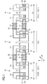
- the switchable capacitors 16 by means of interconnects 52 between the bottom electrodes 18, 22 and interconnects 54 between the substrate remote electrodes 24, 28 to the main capacitor 12 are electrically connected in parallel. Geometrically, however, the switchable capacitors 16 are arranged in a row.
- the interconnects 52 and 54 are in an upper metallization.
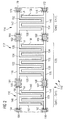
- FIG. 4 shows a transverse electrode 220, to which a recess 222 leads.
- the recess 222 extends approximately over the entire length of the transverse electrode 220. This makes it possible to interrupt the transverse electrode 220 at any point. In other words, the break points can be set continuously along the longitudinal axis of the transverse electrode 220.
Landscapes
- Semiconductor Integrated Circuits (AREA)
- Networks Using Active Elements (AREA)
Claims (6)
- Jeu de condensateurs (110) intégré,
comprenant au moins deux condensateurs intégrés qui sont fabriqués suivant de mêmes plans géométriques et qui comportent respectivement plusieurs électrodes transversales formant une partie principale du condensateur efficace du point de vue de la technique des circuits,
comprenant au moins deux (220) électrodes transversales de correction, disposées en de mêmes positions dans les condensateurs (110) et ayant des longueurs efficaces différentes du point de vue de la technique des circuits,
dans lequel la longueur efficace du point de vue de la technique des circuits d'une électrode (200) transversale de correction est, après la fabrication de la partie principale, diminuée par une interruption (206) isolante du point de vue électrique et/ou par évaporation d'une partie de l'électrode transversale de correction ou est augmentée par une production d'une liaison conductrice d'électricité et,
les condensateurs étant des condensateurs (110) à grille ayant des électrodes en forme de peigne, dont les dents s'interpénètrent. - Condensateurs (110) à grille suivant la revendication 1, caractérisés en ce que dans un matériau recouvrant l'électrode transversale de correction est ménagé au moins un évidement (206, 208 ; 222) qui mène à l'électrode transversale de correction et/ou à une partie sur laquelle l'électrode transversale de correction était disposée avant l'évaporation et/ou en ce que l'évidement (206, 208 ; 222) est rempli d'un matériau passivant.
- Condensateurs (110) à grille suivant la revendication 2, caractérisés en ce que plusieurs évidements (206, 208) mènent à une électrode (220) transversale de correction et,
ou en ce que un évidement, qui recouvre sensiblement toute la partie de l'électrode transversale de correction d'origine, mène a une électrode (220) transversale de correction. - Procédé de production d'un jeu de condensateurs (110) intégré,
dans lequel on fabrique au moins deux condensateurs intégrés suivant les mêmes plans géométriques et on les munit respectivement de plusieurs électrodes transversales qui forment une partie principale du condensateur efficace du point de vue de la technique des circuits,
dans lequel on forme au moins deux électrodes (220) transversales de correction disposées en de mêmes positions dans des électrodes qui sont disposées dans les condensateurs (110) et qui ont des longueurs efficaces différentes du point de vue de la technique des circuits,
et dans lequel on diminue la longueur efficace du point de vue de la technique des circuits d'une électrode (200) transversale de correction après la fabrication de la partie principale par une interruption (206) isolante du point de vue électrique et/ou par évaporation d'une partie de l'électrode transversale de correction ou on l'augmente par production d'une liaison conductrice de l'électricité,
les condensateurs étant des condensateurs (110) à grille ayant des électrodes en forme de peigne, dont les dents s'interpénètrent. - Procédé suivant la revendications 4, caractérisé en ce que l'on ménage dans un matériau recouvrant l'électrode transversale de correction au moins un évidement (206, 208 ; 222) qui mène à l'électrode transversale de correction et/ou à une partie sur laquelle l'électrode transversale de correction a été disposée avant l'évaporation,
et/ou en ce qu'on remplit l'évidement (206, 208 ; 222) d'un matériau passivant. - Procédé suivant la revendication 5, caractérisé en ce que plusieurs évidements (206, 208) mènent à une électrode (220) transversale de correction,
ou en ce que l'évidement qui recouvre sensiblement toute la partie de l'électrode transversale de correction d'origine, mène à une électrode (220) transversale de correction.
Applications Claiming Priority (3)
| Application Number | Priority Date | Filing Date | Title |
|---|---|---|---|
| DE10230697 | 2002-07-08 | ||
| DE10230697 | 2002-07-08 | ||
| EP03762398A EP1520299B1 (fr) | 2002-07-08 | 2003-06-12 | Ensemble d'agencements de condensateurs integres, en particulier de condensateurs de grille integres |
Related Parent Applications (1)
| Application Number | Title | Priority Date | Filing Date |
|---|---|---|---|
| EP03762398A Division EP1520299B1 (fr) | 2002-07-08 | 2003-06-12 | Ensemble d'agencements de condensateurs integres, en particulier de condensateurs de grille integres |
Publications (3)
| Publication Number | Publication Date |
|---|---|
| EP1587145A2 EP1587145A2 (fr) | 2005-10-19 |
| EP1587145A3 EP1587145A3 (fr) | 2007-05-16 |
| EP1587145B1 true EP1587145B1 (fr) | 2009-02-18 |
Family
ID=30009837
Family Applications (2)
| Application Number | Title | Priority Date | Filing Date |
|---|---|---|---|
| EP05106669A Expired - Lifetime EP1587145B1 (fr) | 2002-07-08 | 2003-06-12 | Ensemble d'agencements de condensateurs de grille intégrés et méthode de fabrication correspondante |
| EP03762398A Expired - Lifetime EP1520299B1 (fr) | 2002-07-08 | 2003-06-12 | Ensemble d'agencements de condensateurs integres, en particulier de condensateurs de grille integres |
Family Applications After (1)
| Application Number | Title | Priority Date | Filing Date |
|---|---|---|---|
| EP03762398A Expired - Lifetime EP1520299B1 (fr) | 2002-07-08 | 2003-06-12 | Ensemble d'agencements de condensateurs integres, en particulier de condensateurs de grille integres |
Country Status (7)
| Country | Link |
|---|---|
| US (2) | USRE41684E1 (fr) |
| EP (2) | EP1587145B1 (fr) |
| JP (1) | JP4409428B2 (fr) |
| CN (1) | CN100413074C (fr) |
| DE (2) | DE50311201D1 (fr) |
| TW (1) | TWI226125B (fr) |
| WO (1) | WO2004006334A2 (fr) |
Families Citing this family (8)
| Publication number | Priority date | Publication date | Assignee | Title |
|---|---|---|---|---|
| US20070235880A1 (en) * | 2006-03-30 | 2007-10-11 | Chin-Sheng Yang | Semiconductor device and method of fabricating the same |
| US20090014832A1 (en) * | 2007-07-09 | 2009-01-15 | Peter Baumgartner | Semiconductor Device with Reduced Capacitance Tolerance Value |
| JP2009170903A (ja) * | 2008-01-16 | 2009-07-30 | Hynix Semiconductor Inc | 複数のカッティング部を有するヒューズ及びこれを含むヒューズセット構造 |
| JP2016162925A (ja) * | 2015-03-03 | 2016-09-05 | 力晶科技股▲ふん▼有限公司 | Momキャパシタ回路及び半導体装置 |
| FR3053156B1 (fr) | 2016-06-28 | 2018-11-16 | Stmicroelectronics (Rousset) Sas | Composant a faible dispersion dans une puce electronique |
| US11145591B2 (en) * | 2019-11-18 | 2021-10-12 | International Business Machines Corporation | Integrated circuit (IC) device integral capacitor and anti-fuse |
| US11257750B2 (en) | 2020-02-06 | 2022-02-22 | International Business Machines Corporation | E-fuse co-processed with MIM capacitor |
| US11515247B2 (en) * | 2021-01-14 | 2022-11-29 | Qualcomm Incorporated | Capacitance fine tuning by fin capacitor design |
Family Cites Families (19)
| Publication number | Priority date | Publication date | Assignee | Title |
|---|---|---|---|---|
| US3766308A (en) | 1972-05-25 | 1973-10-16 | Microsystems Int Ltd | Joining conductive elements on microelectronic devices |
| US4152714A (en) * | 1978-01-16 | 1979-05-01 | Honeywell Inc. | Semiconductor apparatus |
| US4190854A (en) * | 1978-02-15 | 1980-02-26 | National Semiconductor Corporation | Trim structure for integrated capacitors |
| DE3124740A1 (de) | 1980-08-14 | 1982-04-08 | VEB Elektronik Gera, DDR 6500 Gera | Verfahren zum abgleichen der kapazitaet elektrischer kondensatoren |
| JPS60121757A (ja) | 1983-12-06 | 1985-06-29 | Nec Corp | 半導体集積回路装置 |
| JPS62155536A (ja) | 1985-12-27 | 1987-07-10 | Casio Comput Co Ltd | トリミング機能付半導体集積回路 |
| US5468680A (en) | 1994-03-18 | 1995-11-21 | Massachusetts Institute Of Technology | Method of making a three-terminal fuse |
| JPH097887A (ja) | 1995-06-16 | 1997-01-10 | Chichibu Onoda Cement Corp | コンデンサ |
| DE19652325C1 (de) | 1996-12-16 | 1998-05-07 | Siemens Ag | Integrierte Halbleiterschaltung mit Kapazitäts-Redundanz |
| JPH10303061A (ja) | 1997-04-25 | 1998-11-13 | Matsushita Electric Ind Co Ltd | 加熱導電性絶縁材料およびその加熱方法 |
| JPH11307389A (ja) * | 1998-04-24 | 1999-11-05 | Mitsubishi Electric Corp | パターンコンデンサ |
| US6198609B1 (en) | 1998-11-09 | 2001-03-06 | Read-Rite Corporation | CPP Magnetoresistive device with reduced edge effect and method for making same |
| JP3292175B2 (ja) | 1999-05-13 | 2002-06-17 | 日本電気株式会社 | 半導体装置 |
| DE19961675A1 (de) | 1999-12-21 | 2001-06-28 | Philips Corp Intellectual Pty | Bauteil mit Dünnschichtschaltkreis mit trimmbarem Kondensator |
| US6680520B2 (en) | 2000-03-14 | 2004-01-20 | International Business Machines Corporation | Method and structure for forming precision MIM fusible circuit elements using fuses and antifuses |
| JP2003535466A (ja) | 2000-06-02 | 2003-11-25 | コーニンクレッカ フィリップス エレクトロニクス エヌ ヴィ | 受動素子 |
| JP3737448B2 (ja) * | 2002-04-18 | 2006-01-18 | Necエレクトロニクス株式会社 | 半導体装置 |
| JP2003323664A (ja) | 2002-05-01 | 2003-11-14 | Nec Soft Ltd | カード決済システム |
| US6839263B2 (en) * | 2003-02-05 | 2005-01-04 | Hewlett-Packard Development Company, L.P. | Memory array with continuous current path through multiple lines |
-
2003
- 2003-05-23 TW TW092114097A patent/TWI226125B/zh not_active IP Right Cessation
- 2003-06-12 US US12/175,170 patent/USRE41684E1/en not_active Expired - Lifetime
- 2003-06-12 JP JP2004518391A patent/JP4409428B2/ja not_active Expired - Fee Related
- 2003-06-12 EP EP05106669A patent/EP1587145B1/fr not_active Expired - Lifetime
- 2003-06-12 DE DE50311201T patent/DE50311201D1/de not_active Expired - Lifetime
- 2003-06-12 EP EP03762398A patent/EP1520299B1/fr not_active Expired - Lifetime
- 2003-06-12 WO PCT/DE2003/001956 patent/WO2004006334A2/fr not_active Ceased
- 2003-06-12 DE DE50305508T patent/DE50305508D1/de not_active Expired - Lifetime
- 2003-06-12 CN CNB038160684A patent/CN100413074C/zh not_active Expired - Fee Related
- 2003-06-12 US US10/520,742 patent/US7079375B2/en not_active Ceased
Also Published As
| Publication number | Publication date |
|---|---|
| JP4409428B2 (ja) | 2010-02-03 |
| EP1587145A3 (fr) | 2007-05-16 |
| USRE41684E1 (en) | 2010-09-14 |
| CN1666343A (zh) | 2005-09-07 |
| EP1520299B1 (fr) | 2006-10-25 |
| WO2004006334A2 (fr) | 2004-01-15 |
| DE50305508D1 (de) | 2006-12-07 |
| EP1587145A2 (fr) | 2005-10-19 |
| TW200401431A (en) | 2004-01-16 |
| DE50311201D1 (de) | 2009-04-02 |
| TWI226125B (en) | 2005-01-01 |
| US7079375B2 (en) | 2006-07-18 |
| WO2004006334A3 (fr) | 2004-04-08 |
| EP1520299A2 (fr) | 2005-04-06 |
| JP2005538533A (ja) | 2005-12-15 |
| CN100413074C (zh) | 2008-08-20 |
| US20060097580A1 (en) | 2006-05-11 |
Similar Documents
| Publication | Publication Date | Title |
|---|---|---|
| EP1573819B1 (fr) | Procede de production d'un systeme condensateur et systeme condensateur | |
| DE4020195C2 (de) | Verfahren zur Vereinzelung von Halbleiterchips | |
| DE69621011T2 (de) | Kondensator für eine integrierte schaltung | |
| DE68917489T2 (de) | Abgleichwiderstandsnetzwerk. | |
| DE69526630T2 (de) | Verbesserungen in oder in Beziehung auf integrierte Schaltungen | |
| DE102008054073A1 (de) | Halbleiterbauelement mit elektronischen Sicherungen mit erhöhter Programmiereffizienz | |
| EP2122671A1 (fr) | Dispositif à semi-conducteurs comportant un condensateur à tranchées et procédé de fabrication | |
| DE112018000336T5 (de) | Kondensator | |
| DE10046910A1 (de) | Halbleitervorrichtung | |
| DE4341698B4 (de) | Halbleiterbauelement mit einem Speicherkondensator und Verfahren zu dessen Herstellung | |
| DE2901511A1 (de) | Halbleiteranordnung | |
| DE69226223T2 (de) | Kontaktausrichtung für Festwertspeicher | |
| EP1520299B1 (fr) | Ensemble d'agencements de condensateurs integres, en particulier de condensateurs de grille integres | |
| DE10158798A1 (de) | Kondensator und Verfahren zum Herstellen eines Kondensators | |
| WO2000042657A1 (fr) | Composant electronique et utilisation d'une structure de protection a l'interieur dudit composant | |
| DE102011100779B4 (de) | Elektronische Vorrichtung und Verfahren zur Herstellung einer elektronischen Vorrichtung | |
| EP2040298B1 (fr) | Circuits intégrés comprenant un condensateur qui résiste aux décharges électrostatiques et procédé de réalisation | |
| DE102018126026A1 (de) | Akkumulationsverstärkter bipolartransistor mit isolierter gate-elektrode (accumulation enhanced insulated gate bipolar transistor, aegt) und verfahren zu dessen verwendung | |
| DE102005046734B4 (de) | Halbleiterbauelement mit integrierter Kapazitätsstruktur | |
| EP1261989B1 (fr) | Condensateur metal-isolant-metal et son procede de production | |
| DE3930622C2 (de) | Statischer RAM | |
| DE102004060369A1 (de) | Halbleiterscheibe mit Teststruktur | |
| DE102020005807A1 (de) | Halbleitersicherungsstruktur und verfahren zum herstellen einer halbleitersicherungsstruktur | |
| EP0749156A1 (fr) | Dispositif semi-conducteur comportant des contacts auto-alignés et son procédé de fabrication | |
| WO2001063652A1 (fr) | Composant semi-conducteur et procede de fabrication dudit composant |
Legal Events
| Date | Code | Title | Description |
|---|---|---|---|
| PUAI | Public reference made under article 153(3) epc to a published international application that has entered the european phase |
Free format text: ORIGINAL CODE: 0009012 |
|
| AC | Divisional application: reference to earlier application |
Ref document number: 1520299 Country of ref document: EP Kind code of ref document: P |
|
| AK | Designated contracting states |
Kind code of ref document: A2 Designated state(s): DE FR |
|
| PUAL | Search report despatched |
Free format text: ORIGINAL CODE: 0009013 |
|
| AK | Designated contracting states |
Kind code of ref document: A3 Designated state(s): DE FR |
|
| 17P | Request for examination filed |
Effective date: 20070618 |
|
| 17Q | First examination report despatched |
Effective date: 20070806 |
|
| AKX | Designation fees paid |
Designated state(s): DE FR |
|
| GRAP | Despatch of communication of intention to grant a patent |
Free format text: ORIGINAL CODE: EPIDOSNIGR1 |
|
| RIC1 | Information provided on ipc code assigned before grant |
Ipc: H01L 27/08 20060101AFI20080814BHEP Ipc: H01L 21/02 20060101ALI20080814BHEP |
|
| RTI1 | Title (correction) |
Free format text: SET OF INTEGRATED GRID CAPACITORS AND METHOD OF MANUFACTURING THE SAME |
|
| GRAS | Grant fee paid |
Free format text: ORIGINAL CODE: EPIDOSNIGR3 |
|
| GRAA | (expected) grant |
Free format text: ORIGINAL CODE: 0009210 |
|
| AC | Divisional application: reference to earlier application |
Ref document number: 1520299 Country of ref document: EP Kind code of ref document: P |
|
| AK | Designated contracting states |
Kind code of ref document: B1 Designated state(s): DE FR |
|
| REF | Corresponds to: |
Ref document number: 50311201 Country of ref document: DE Date of ref document: 20090402 Kind code of ref document: P |
|
| PLBE | No opposition filed within time limit |
Free format text: ORIGINAL CODE: 0009261 |
|
| STAA | Information on the status of an ep patent application or granted ep patent |
Free format text: STATUS: NO OPPOSITION FILED WITHIN TIME LIMIT |
|
| 26N | No opposition filed |
Effective date: 20091119 |
|
| REG | Reference to a national code |
Ref country code: FR Ref legal event code: ST Effective date: 20100226 |
|
| PG25 | Lapsed in a contracting state [announced via postgrant information from national office to epo] |
Ref country code: FR Free format text: LAPSE BECAUSE OF NON-PAYMENT OF DUE FEES Effective date: 20090630 |
|
| PGFP | Annual fee paid to national office [announced via postgrant information from national office to epo] |
Ref country code: DE Payment date: 20170822 Year of fee payment: 15 |
|
| REG | Reference to a national code |
Ref country code: DE Ref legal event code: R119 Ref document number: 50311201 Country of ref document: DE |
|
| PG25 | Lapsed in a contracting state [announced via postgrant information from national office to epo] |
Ref country code: DE Free format text: LAPSE BECAUSE OF NON-PAYMENT OF DUE FEES Effective date: 20190101 |