EP1590721B1 - Elektronische vorrichtung - Google Patents
Elektronische vorrichtung Download PDFInfo
- Publication number
- EP1590721B1 EP1590721B1 EP04705146A EP04705146A EP1590721B1 EP 1590721 B1 EP1590721 B1 EP 1590721B1 EP 04705146 A EP04705146 A EP 04705146A EP 04705146 A EP04705146 A EP 04705146A EP 1590721 B1 EP1590721 B1 EP 1590721B1
- Authority
- EP
- European Patent Office
- Prior art keywords
- electrode
- electronic device
- transistor
- source
- active layer
- Prior art date
- Legal status (The legal status is an assumption and is not a legal conclusion. Google has not performed a legal analysis and makes no representation as to the accuracy of the status listed.)
- Expired - Lifetime
Links
Images


Classifications
-
- H—ELECTRICITY
- H10—SEMICONDUCTOR DEVICES; ELECTRIC SOLID-STATE DEVICES NOT OTHERWISE PROVIDED FOR
- H10K—ORGANIC ELECTRIC SOLID-STATE DEVICES
- H10K19/00—Integrated devices, or assemblies of multiple devices, comprising at least one organic element specially adapted for rectifying, amplifying, oscillating or switching, covered by group H10K10/00
- H10K19/10—Integrated devices, or assemblies of multiple devices, comprising at least one organic element specially adapted for rectifying, amplifying, oscillating or switching, covered by group H10K10/00 comprising field-effect transistors
-
- B—PERFORMING OPERATIONS; TRANSPORTING
- B82—NANOTECHNOLOGY
- B82Y—SPECIFIC USES OR APPLICATIONS OF NANOSTRUCTURES; MEASUREMENT OR ANALYSIS OF NANOSTRUCTURES; MANUFACTURE OR TREATMENT OF NANOSTRUCTURES
- B82Y10/00—Nanotechnology for information processing, storage or transmission, e.g. quantum computing or single electron logic
-
- H—ELECTRICITY
- H10—SEMICONDUCTOR DEVICES; ELECTRIC SOLID-STATE DEVICES NOT OTHERWISE PROVIDED FOR
- H10K—ORGANIC ELECTRIC SOLID-STATE DEVICES
- H10K10/00—Organic devices specially adapted for rectifying, amplifying, oscillating or switching; Organic capacitors or resistors having potential barriers
- H10K10/40—Organic transistors
- H10K10/46—Field-effect transistors, e.g. organic thin-film transistors [OTFT]
- H10K10/462—Insulated gate field-effect transistors [IGFETs]
- H10K10/466—Lateral bottom-gate IGFETs comprising only a single gate
-
- H—ELECTRICITY
- H10—SEMICONDUCTOR DEVICES; ELECTRIC SOLID-STATE DEVICES NOT OTHERWISE PROVIDED FOR
- H10K—ORGANIC ELECTRIC SOLID-STATE DEVICES
- H10K10/00—Organic devices specially adapted for rectifying, amplifying, oscillating or switching; Organic capacitors or resistors having potential barriers
- H10K10/40—Organic transistors
- H10K10/46—Field-effect transistors, e.g. organic thin-film transistors [OTFT]
- H10K10/462—Insulated gate field-effect transistors [IGFETs]
- H10K10/468—Insulated gate field-effect transistors [IGFETs] characterised by the gate dielectrics
-
- H—ELECTRICITY
- H10—SEMICONDUCTOR DEVICES; ELECTRIC SOLID-STATE DEVICES NOT OTHERWISE PROVIDED FOR
- H10K—ORGANIC ELECTRIC SOLID-STATE DEVICES
- H10K10/00—Organic devices specially adapted for rectifying, amplifying, oscillating or switching; Organic capacitors or resistors having potential barriers
- H10K10/40—Organic transistors
- H10K10/46—Field-effect transistors, e.g. organic thin-film transistors [OTFT]
- H10K10/462—Insulated gate field-effect transistors [IGFETs]
- H10K10/484—Insulated gate field-effect transistors [IGFETs] characterised by the channel regions
- H10K10/488—Insulated gate field-effect transistors [IGFETs] characterised by the channel regions the channel region comprising a layer of composite material having interpenetrating or embedded materials, e.g. a mixture of donor and acceptor moieties, that form a bulk heterojunction
-
- H—ELECTRICITY
- H10—SEMICONDUCTOR DEVICES; ELECTRIC SOLID-STATE DEVICES NOT OTHERWISE PROVIDED FOR
- H10K—ORGANIC ELECTRIC SOLID-STATE DEVICES
- H10K85/00—Organic materials used in the body or electrodes of devices covered by this subclass
- H10K85/10—Organic polymers or oligomers
- H10K85/111—Organic polymers or oligomers comprising aromatic, heteroaromatic, or aryl chains, e.g. polyaniline, polyphenylene or polyphenylene vinylene
- H10K85/114—Poly-phenylenevinylene; Derivatives thereof
-
- H—ELECTRICITY
- H10—SEMICONDUCTOR DEVICES; ELECTRIC SOLID-STATE DEVICES NOT OTHERWISE PROVIDED FOR
- H10K—ORGANIC ELECTRIC SOLID-STATE DEVICES
- H10K85/00—Organic materials used in the body or electrodes of devices covered by this subclass
- H10K85/10—Organic polymers or oligomers
- H10K85/111—Organic polymers or oligomers comprising aromatic, heteroaromatic, or aryl chains, e.g. polyaniline, polyphenylene or polyphenylene vinylene
- H10K85/115—Polyfluorene; Derivatives thereof
-
- H—ELECTRICITY
- H10—SEMICONDUCTOR DEVICES; ELECTRIC SOLID-STATE DEVICES NOT OTHERWISE PROVIDED FOR
- H10K—ORGANIC ELECTRIC SOLID-STATE DEVICES
- H10K85/00—Organic materials used in the body or electrodes of devices covered by this subclass
- H10K85/20—Carbon compounds, e.g. carbon nanotubes or fullerenes
- H10K85/211—Fullerenes, e.g. C60
-
- H—ELECTRICITY
- H10—SEMICONDUCTOR DEVICES; ELECTRIC SOLID-STATE DEVICES NOT OTHERWISE PROVIDED FOR
- H10K—ORGANIC ELECTRIC SOLID-STATE DEVICES
- H10K85/00—Organic materials used in the body or electrodes of devices covered by this subclass
- H10K85/30—Coordination compounds
- H10K85/331—Metal complexes comprising an iron-series metal, e.g. Fe, Co, Ni
-
- H—ELECTRICITY
- H10—SEMICONDUCTOR DEVICES; ELECTRIC SOLID-STATE DEVICES NOT OTHERWISE PROVIDED FOR
- H10K—ORGANIC ELECTRIC SOLID-STATE DEVICES
- H10K85/00—Organic materials used in the body or electrodes of devices covered by this subclass
- H10K85/60—Organic compounds having low molecular weight
-
- H—ELECTRICITY
- H10—SEMICONDUCTOR DEVICES; ELECTRIC SOLID-STATE DEVICES NOT OTHERWISE PROVIDED FOR
- H10K—ORGANIC ELECTRIC SOLID-STATE DEVICES
- H10K85/00—Organic materials used in the body or electrodes of devices covered by this subclass
- H10K85/60—Organic compounds having low molecular weight
- H10K85/615—Polycyclic condensed aromatic hydrocarbons, e.g. anthracene
- H10K85/626—Polycyclic condensed aromatic hydrocarbons, e.g. anthracene containing more than one polycyclic condensed aromatic rings, e.g. bis-anthracene
-
- H—ELECTRICITY
- H10—SEMICONDUCTOR DEVICES; ELECTRIC SOLID-STATE DEVICES NOT OTHERWISE PROVIDED FOR
- H10K—ORGANIC ELECTRIC SOLID-STATE DEVICES
- H10K85/00—Organic materials used in the body or electrodes of devices covered by this subclass
- H10K85/60—Organic compounds having low molecular weight
- H10K85/649—Aromatic compounds comprising a hetero atom
- H10K85/653—Aromatic compounds comprising a hetero atom comprising only oxygen as heteroatom
Definitions
- a disadvantage of the known device is that such a device with unipolar logics must be connected to an inverter unit.
- such a unit comprises two transistors whose drain electrodes are interconnected, and in which the gate of one transistor, the load transistor, is electrically connected with the drain electrodes. The drain electrodes are then connected with the output of the inverter, the source electrode of the load transistor to the supply voltage V dd , the gate electrode of the second, driver, transistor is connected with the input, and the source electrode of the control transistor is grounded.
- an active layer with in this instance a blend of polyphenylenevinylene and buckminsterfullerene has a known use in solar cells.
- the active layer is used to receive light and to convert a photon into an electron and a hole, which holes are subsequently transported to the electrodes. This creates simultaneous transport of electrons and holes in opposite directions.
- the device according to the invention may also be suitable for other applications; in particular for memory circuits, such as SRAM and DRAM, for ring oscillators, for identification purposes, etc., as is known to the specialist in the field of circuitry.
- memory circuits such as SRAM and DRAM, for ring oscillators, for identification purposes, etc., as is known to the specialist in the field of circuitry.
- the drain electrodes of the first and second transistor are common; that is to say that there is only one single drain electrode.
- the use of an interdigitated electrode pair is advantageous in that a greater channel width is achieved, whereas the surface of the transistor or the inverter does not increase accordingly. It is self-evidently simple to enlarge the finger-like structure of the drain electrode, so that both source electrodes connect to it.
- the source electrodes are not on the same voltage, which might lead to parasites and uncontrollable effects. In order to prevent this, the source electrodes are mutually screened by intermediate parts of the drain electrode. In this way the parasitic effects are controllable.
- the screening by the drain electrode is achieved for example in that two or more finger-like structures of the drain electrode are present between the source electrodes.
- the drain electrode preferably has a body with a first side and a second side turned away from this first side, which body on the first and second side has a finger-like structure.
- the source electrode is then located on the first side and forms an interdigitated electrode pair with the finger-like structure on this first side.
- the drain electrode is located on the second side and forms an interdigitated electrode pair with the finger-like structure on this second side.
- the intermediate layer 4 contains in general a photostructurable organic dielectric, such as benzocyclobutene, polyimide, polyvinylphenol or a photoresist, such as SU8.
- the intermediate layer may also contain an inorganic dielectric, such as for example SiO 2 , which was the case in a first experiment.
- the photoresist SU8 was applied as an intermediate layer.
- the first electrode layer 2 contains gold in this case.
- the first electrode layer 2 is applied by means of spin coating and structured by exposure.
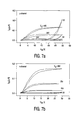
- Fig. 5 shows the transfer characteristics of the inverter according to the invention, where two identical transistors are applied.
- the applied transistors have an active layer with a blend of [6,6]-phenyl C61 butyric acid methylester and of OC 1 OC 10 -PPV.
- the applied transistors are described with reference to Fig. 2.
- the inverter operates according to the invention in the first or the third quadrant.
- An inverter based on unipolar logics on the other hand, operates only in the first quadrant.
- a small increase in the output voltage V out can be observed at low and at high values of the input voltage V IN .
Landscapes
- Chemical & Material Sciences (AREA)
- Engineering & Computer Science (AREA)
- Materials Engineering (AREA)
- Physics & Mathematics (AREA)
- Spectroscopy & Molecular Physics (AREA)
- Nanotechnology (AREA)
- Inorganic Chemistry (AREA)
- Mathematical Physics (AREA)
- Theoretical Computer Science (AREA)
- Crystallography & Structural Chemistry (AREA)
- Composite Materials (AREA)
- Thin Film Transistor (AREA)
- Metal-Oxide And Bipolar Metal-Oxide Semiconductor Integrated Circuits (AREA)
- Heterocyclic Carbon Compounds Containing A Hetero Ring Having Oxygen Or Sulfur (AREA)
- Fixed Capacitors And Capacitor Manufacturing Machines (AREA)
- Thermistors And Varistors (AREA)
- Surgical Instruments (AREA)
- Valve Device For Special Equipments (AREA)
- Noodles (AREA)
- Semiconductor Memories (AREA)
Claims (9)
- Elektronische Anordnung mit einer Wechselrichtereinheit (10) mit einem ersten (11) und einem zweiten (12) Feldeffekttransistor, welche jeweils eine Source- (21, 21') und eine Drainelektrode (22, 22') aufweisen, wobei die Elektroden der Feldeffekttransistoren in der gleichen Elektrodenschicht (2) aus elektrisch leitendem Material vorgesehen sind und das Source- und Drainelektrodenpaar durch einen ersten Kanal (23) vom n-Leitfähigkeitstyp und durch einen zweiten Kanal (23') vom p-Leitfähigkeitstyp untereinander verbunden sind, wobei die Kanäle in einer aktiven Schicht vorgesehen sind, welche organisches Halbleitermaterial enthält und welche von dem ersten und dem zweiten Transistor gemeinsam genutzt wird, wobei jeder der Transistoren eine Gateelektrode (24, 24') aufweist, welche durch eine dielektrische Schicht (4) von den Kanälen getrennt ist.
- Elektronische Anordnung nach Anspruch 1, dadurch gekennzeichnet, dass eine gemeinsame Gateelektrode für den ersten und den zweiten Transistor vorhanden ist.
- Elektronische Anordnung nach Anspruch 1 oder 2, dadurch gekennzeichnet, dass die Drainelektroden des ersten und des zweiten Transistors gemeinsam genutzt werden.
- Elektronische Anordnung nach Anspruch 3, dadurch gekennzeichnet, dass die Source- und Drainelektrode ein interdigitierendes Elektrodenpaar bilden, bei welchem die Sourceelektroden durch Zwischenteile der Drainelektrode gegenseitig geschützt sind.
- Elektronische Anordnung nach Anspruch 4, dadurch gekennzeichnet, dass die Drainelektrode einen Körper mit einer ersten Seite und einer von dieser ersten Seite abgewandten, zweiten Seite aufweist, welcher auf der ersten Seite und der zweiten Seite fingerartige Strukturen besitzt, wobei die Sourceelektrode auf der ersten Seite vorgesehen ist und zusammen mit der fingerartigen Struktur auf dieser ersten Seite ein interdigitierendes Elektrodenpaar bildet, und wobei die Drainelektrode auf der zweiten Seite vorgesehen ist und zusammen mit der fingerartigen Struktur auf dieser zweiten Seite ebenfalls ein interdigitierendes Elektrodenpaar bildet.
- Elektronische Anordnung nach Anspruch 1, dadurch gekennzeichnet, dass die aktive Schicht ein Gemisch aus einem organischen Trägermaterial, dem p-leitenden Halbleitermaterial und dem n-leitenden Halbleitermaterial enthält.
- Elektronische Anordnung nach Anspruch 1, dadurch gekennzeichnet, dass die Source- und Drainelektrode ein aus der Gruppe von Edelmetallen ausgewähltes Material enthalten.
- Elektronische Anordnung nach Anspruch 1, dadurch gekennzeichnet, dass das n- und p-leitende Halbleitermaterial eine Mobilität µn, µp in einem gegenseitigen Verhältnis im Bereich von 0,1 bis 10 aufweist.
- Verfahren zur Herstellung einer elektronischen Anordnung mit einer Wechselrichtereinheit mit einem ersten und einem zweiten Feldeffekttransistor mit einer gemeinsamen aktiven Schicht, welche ein funktionalisiertes, organisches, n-leitendes Halbleitermaterial und ein funktionalisiertes, organisches, p-leitendes Halbleitermaterial enthält, wobei die aktive Schicht aus einer Lösung auf ein Substrat aufgetragen wird.
Priority Applications (1)
| Application Number | Priority Date | Filing Date | Title |
|---|---|---|---|
| EP04705146A EP1590721B1 (de) | 2003-01-28 | 2004-01-26 | Elektronische vorrichtung |
Applications Claiming Priority (4)
| Application Number | Priority Date | Filing Date | Title |
|---|---|---|---|
| EP03100177 | 2003-01-28 | ||
| EP03100177 | 2003-01-28 | ||
| PCT/IB2004/050053 WO2004068267A2 (en) | 2003-01-28 | 2004-01-26 | Electronic device |
| EP04705146A EP1590721B1 (de) | 2003-01-28 | 2004-01-26 | Elektronische vorrichtung |
Publications (2)
| Publication Number | Publication Date |
|---|---|
| EP1590721A2 EP1590721A2 (de) | 2005-11-02 |
| EP1590721B1 true EP1590721B1 (de) | 2007-04-11 |
Family
ID=32798988
Family Applications (2)
| Application Number | Title | Priority Date | Filing Date |
|---|---|---|---|
| EP04705146A Expired - Lifetime EP1590721B1 (de) | 2003-01-28 | 2004-01-26 | Elektronische vorrichtung |
| EP04705480A Expired - Lifetime EP1590839B1 (de) | 2003-01-28 | 2004-01-27 | Elektronisches bauteil |
Family Applications After (1)
| Application Number | Title | Priority Date | Filing Date |
|---|---|---|---|
| EP04705480A Expired - Lifetime EP1590839B1 (de) | 2003-01-28 | 2004-01-27 | Elektronisches bauteil |
Country Status (8)
| Country | Link |
|---|---|
| US (2) | US20060243965A1 (de) |
| EP (2) | EP1590721B1 (de) |
| JP (1) | JP2006518938A (de) |
| KR (1) | KR20050096162A (de) |
| CN (2) | CN1742392A (de) |
| AT (2) | ATE359545T1 (de) |
| DE (2) | DE602004005824T2 (de) |
| WO (2) | WO2004068267A2 (de) |
Families Citing this family (21)
| Publication number | Priority date | Publication date | Assignee | Title |
|---|---|---|---|---|
| DE102004008784B3 (de) * | 2004-02-23 | 2005-09-15 | Infineon Technologies Ag | Verfahren zur Durchkontaktierung von Feldeffekttransistoren mit einer selbstorganisierten Monolage einer organischen Verbindung als Gatedielektrikum |
| JP4661065B2 (ja) * | 2004-03-22 | 2011-03-30 | セイコーエプソン株式会社 | 相補型有機半導体装置 |
| TWI228833B (en) * | 2004-05-04 | 2005-03-01 | Ind Tech Res Inst | Method for enhancing the electrical characteristics of organic electronic devices |
| DE102004059467A1 (de) * | 2004-12-10 | 2006-07-20 | Polyic Gmbh & Co. Kg | Gatter aus organischen Feldeffekttransistoren |
| KR100585629B1 (ko) * | 2005-02-04 | 2006-06-07 | 삼성전자주식회사 | 신뢰성을 향상시키는 안티퓨즈 회로 및 이를 이용한안티퓨징 방법 |
| DE102005034414B4 (de) * | 2005-07-22 | 2007-11-15 | Siemens Ag | Verwendung eines lösungsprozessierbaren Materials als aktive halbleitende Schicht in einem n-Typ-Transistor |
| US20070146426A1 (en) * | 2005-12-28 | 2007-06-28 | Nelson Brian K | All-inkjet printed thin film transistor |
| TWI345326B (en) * | 2006-03-29 | 2011-07-11 | Pioneer Corp | Organic thin film transistor device and manufacturing method therefor |
| US8247801B2 (en) * | 2006-03-31 | 2012-08-21 | Imec | Organic semi-conductor photo-detecting device |
| US20070286953A1 (en) * | 2006-05-20 | 2007-12-13 | Macpherson Charles D | Solution processible materials and their use in electronic devices |
| KR100943146B1 (ko) * | 2007-02-13 | 2010-02-18 | 주식회사 엘지화학 | 티아졸로티아졸 유도체를 이용한 유기 트랜지스터 및 이의제조방법 |
| US8129714B2 (en) * | 2007-02-16 | 2012-03-06 | Idemitsu Kosan Co., Ltd. | Semiconductor, semiconductor device, complementary transistor circuit device |
| GB0706756D0 (en) * | 2007-04-05 | 2007-05-16 | Imp Innovations Ltd | Improvements in organic field-effect transistors |
| US7652339B2 (en) * | 2007-04-06 | 2010-01-26 | Xerox Corporation | Ambipolar transistor design |
| DE102009043348B4 (de) * | 2009-09-29 | 2012-12-13 | Siemens Aktiengesellschaft | Material für eine photoaktive Schicht in organischen Photodioden, Verwendung dazu, sowie eine organische Photodiode |
| EP2810313B1 (de) * | 2012-02-02 | 2017-06-14 | Basf Se | Verfahren zur herstellung eines organischen halbleiterbauelements |
| US10005879B2 (en) | 2012-02-03 | 2018-06-26 | Basf Se | Method for producing an organic semiconductor device |
| US9147615B2 (en) | 2014-02-14 | 2015-09-29 | International Business Machines Corporation | Ambipolar synaptic devices |
| US10692863B2 (en) | 2016-09-30 | 2020-06-23 | Rohm Co., Ltd. | Semiconductor device and semiconductor package |
| US10475698B2 (en) * | 2017-03-31 | 2019-11-12 | Teresa Oh | Ambipolar transistor and electronic sensor of high sensitivity using the same |
| KR102363387B1 (ko) * | 2020-01-21 | 2022-02-15 | 금오공과대학교 산학협력단 | 불소 처리 그래핀을 이용한 2차원 구조 센서 |
Family Cites Families (19)
| Publication number | Priority date | Publication date | Assignee | Title |
|---|---|---|---|---|
| JP2813428B2 (ja) * | 1989-08-17 | 1998-10-22 | 三菱電機株式会社 | 電界効果トランジスタ及び該電界効果トランジスタを用いた液晶表示装置 |
| JP3522771B2 (ja) * | 1991-03-22 | 2004-04-26 | 三菱電機株式会社 | インバータ |
| US5380807A (en) * | 1992-01-15 | 1995-01-10 | U.S. Philips Corporation | Electrically conductive alternating copolymer and method of preparing such a copolymer |
| JP3246189B2 (ja) * | 1994-06-28 | 2002-01-15 | 株式会社日立製作所 | 半導体表示装置 |
| US6278127B1 (en) * | 1994-12-09 | 2001-08-21 | Agere Systems Guardian Corp. | Article comprising an organic thin film transistor adapted for biasing to form a N-type or a P-type transistor |
| US5574291A (en) * | 1994-12-09 | 1996-11-12 | Lucent Technologies Inc. | Article comprising a thin film transistor with low conductivity organic layer |
| TW293172B (de) * | 1994-12-09 | 1996-12-11 | At & T Corp | |
| JPH0974217A (ja) * | 1995-09-07 | 1997-03-18 | Nippon Shokubai Co Ltd | 有機太陽電池 |
| US5625199A (en) * | 1996-01-16 | 1997-04-29 | Lucent Technologies Inc. | Article comprising complementary circuit with inorganic n-channel and organic p-channel thin film transistors |
| EP0968537B1 (de) * | 1997-08-22 | 2012-05-02 | Creator Technology B.V. | Feld-effekt-transistor, der im wesentlichen aus organischen materialien besteht |
| JP2004538618A (ja) * | 1999-10-11 | 2004-12-24 | コーニンクレッカ フィリップス エレクトロニクス エヌ ヴィ | 集積回路 |
| US6284562B1 (en) * | 1999-11-17 | 2001-09-04 | Agere Systems Guardian Corp. | Thin film transistors |
| US6429040B1 (en) * | 2000-04-06 | 2002-08-06 | Agere Systems Guardian Corp. | Device comprising a bipolar semi-conducting film |
| US6452207B1 (en) * | 2001-03-30 | 2002-09-17 | Lucent Technologies Inc. | Organic semiconductor devices |
| JP2002326305A (ja) * | 2001-04-27 | 2002-11-12 | Nisshinbo Ind Inc | 透視性電磁波シールド板、その製造方法及びディスプレイ装置 |
| US6794220B2 (en) * | 2001-09-05 | 2004-09-21 | Konica Corporation | Organic thin-film semiconductor element and manufacturing method for the same |
| JP2005505142A (ja) * | 2001-10-01 | 2005-02-17 | コーニンクレッカ フィリップス エレクトロニクス エヌ ヴィ | 電子デバイス及び構成並びに方法 |
| EP1306909A1 (de) * | 2001-10-24 | 2003-05-02 | Interuniversitair Micro-Elektronica Centrum | Ambipolarer organischer Transistor |
| US6555411B1 (en) * | 2001-12-18 | 2003-04-29 | Lucent Technologies Inc. | Thin film transistors |
-
2004
- 2004-01-26 US US10/543,277 patent/US20060243965A1/en not_active Abandoned
- 2004-01-26 CN CN200480002935.8A patent/CN1742392A/zh active Pending
- 2004-01-26 DE DE602004005824T patent/DE602004005824T2/de not_active Expired - Fee Related
- 2004-01-26 KR KR1020057013847A patent/KR20050096162A/ko not_active Withdrawn
- 2004-01-26 AT AT04705146T patent/ATE359545T1/de not_active IP Right Cessation
- 2004-01-26 EP EP04705146A patent/EP1590721B1/de not_active Expired - Lifetime
- 2004-01-26 JP JP2006502543A patent/JP2006518938A/ja active Pending
- 2004-01-26 WO PCT/IB2004/050053 patent/WO2004068267A2/en not_active Ceased
- 2004-01-27 CN CN200480002930.5A patent/CN1742393B/zh not_active Expired - Fee Related
- 2004-01-27 WO PCT/IB2004/050055 patent/WO2004068609A1/en not_active Ceased
- 2004-01-27 US US10/543,276 patent/US7750339B2/en not_active Expired - Fee Related
- 2004-01-27 AT AT04705480T patent/ATE489730T1/de not_active IP Right Cessation
- 2004-01-27 EP EP04705480A patent/EP1590839B1/de not_active Expired - Lifetime
- 2004-01-27 DE DE602004030214T patent/DE602004030214D1/de not_active Expired - Lifetime
Also Published As
| Publication number | Publication date |
|---|---|
| US20060163561A1 (en) | 2006-07-27 |
| CN1742392A (zh) | 2006-03-01 |
| US7750339B2 (en) | 2010-07-06 |
| DE602004005824D1 (de) | 2007-05-24 |
| EP1590839B1 (de) | 2010-11-24 |
| WO2004068609A1 (en) | 2004-08-12 |
| CN1742393B (zh) | 2011-12-28 |
| EP1590721A2 (de) | 2005-11-02 |
| DE602004005824T2 (de) | 2008-01-10 |
| ATE489730T1 (de) | 2010-12-15 |
| CN1742393A (zh) | 2006-03-01 |
| WO2004068267A3 (en) | 2004-09-16 |
| US20060243965A1 (en) | 2006-11-02 |
| WO2004068267A2 (en) | 2004-08-12 |
| DE602004030214D1 (de) | 2011-01-05 |
| KR20050096162A (ko) | 2005-10-05 |
| EP1590839A1 (de) | 2005-11-02 |
| JP2006518938A (ja) | 2006-08-17 |
| ATE359545T1 (de) | 2007-05-15 |
Similar Documents
| Publication | Publication Date | Title |
|---|---|---|
| US20060243965A1 (en) | Electronic device | |
| KR100970186B1 (ko) | 유기 전계 효과 트랜지스터 | |
| KR101943595B1 (ko) | 액티브 매트릭스 감쇄 소스 인에이블형 수직 유기 발광 트랜지스터 | |
| US9741901B2 (en) | Two-terminal electronic devices and their methods of fabrication | |
| US7208756B2 (en) | Organic semiconductor devices having low contact resistance | |
| US7476893B2 (en) | Vertical organic field effect transistor | |
| EP1051762A1 (de) | X-y adressierbare elektrische mikroschalteranordnung und seine verwendung in sensormatrizen | |
| EP1665355B1 (de) | Elektronische bauelemente | |
| US8569746B2 (en) | Organic field effect transistor | |
| KR20090040199A (ko) | 다층 바이폴라 전계효과 트랜지스터 및 그의 제조방법 | |
| KR20070085953A (ko) | 유기 전계 효과 트랜지스터 게이트 | |
| CN1674320B (zh) | 有机场效应晶体管及制造方法和含该晶体管的平板显示器 | |
| US8552421B2 (en) | Organic microelectronic device and fabrication method therefor | |
| US7321133B2 (en) | Heteroatomic regioregular poly(3-substitutedthiophenes) as thin film conductors in diodes which are not light emitting or photovoltaic | |
| JP2008243911A (ja) | 有機薄膜トランジスタ及びディスプレイ | |
| EP1648040B1 (de) | Chemischer Dünnschichttransistor und seine Herstellung | |
| US8642379B2 (en) | Thin film transistor | |
| US20070241325A1 (en) | Schottky Gate Organic Field Effect Transistor and Fabrication Method of the Same | |
| US20040262601A1 (en) | Organic field-effect transistor and method of manufacturing same | |
| Larsson | Empirical parameterization of organic electrochemical transistors | |
| US20090146136A1 (en) | Organic memory device and method of fabricating the same |
Legal Events
| Date | Code | Title | Description |
|---|---|---|---|
| PUAI | Public reference made under article 153(3) epc to a published international application that has entered the european phase |
Free format text: ORIGINAL CODE: 0009012 |
|
| 17P | Request for examination filed |
Effective date: 20050829 |
|
| AK | Designated contracting states |
Kind code of ref document: A2 Designated state(s): AT BE BG CH CY CZ DE DK EE ES FI FR GB GR HU IE IT LI LU MC NL PT RO SE SI SK TR |
|
| AX | Request for extension of the european patent |
Extension state: AL LT LV MK |
|
| DAX | Request for extension of the european patent (deleted) | ||
| GRAP | Despatch of communication of intention to grant a patent |
Free format text: ORIGINAL CODE: EPIDOSNIGR1 |
|
| GRAS | Grant fee paid |
Free format text: ORIGINAL CODE: EPIDOSNIGR3 |
|
| GRAA | (expected) grant |
Free format text: ORIGINAL CODE: 0009210 |
|
| AK | Designated contracting states |
Kind code of ref document: B1 Designated state(s): AT BE BG CH CY CZ DE DK EE ES FI FR GB GR HU IE IT LI LU MC NL PT RO SE SI SK TR |
|
| PG25 | Lapsed in a contracting state [announced via postgrant information from national office to epo] |
Ref country code: LI Free format text: LAPSE BECAUSE OF FAILURE TO SUBMIT A TRANSLATION OF THE DESCRIPTION OR TO PAY THE FEE WITHIN THE PRESCRIBED TIME-LIMIT Effective date: 20070411 Ref country code: SI Free format text: LAPSE BECAUSE OF FAILURE TO SUBMIT A TRANSLATION OF THE DESCRIPTION OR TO PAY THE FEE WITHIN THE PRESCRIBED TIME-LIMIT Effective date: 20070411 Ref country code: FI Free format text: LAPSE BECAUSE OF FAILURE TO SUBMIT A TRANSLATION OF THE DESCRIPTION OR TO PAY THE FEE WITHIN THE PRESCRIBED TIME-LIMIT Effective date: 20070411 Ref country code: CH Free format text: LAPSE BECAUSE OF FAILURE TO SUBMIT A TRANSLATION OF THE DESCRIPTION OR TO PAY THE FEE WITHIN THE PRESCRIBED TIME-LIMIT Effective date: 20070411 |
|
| REG | Reference to a national code |
Ref country code: GB Ref legal event code: FG4D |
|
| REG | Reference to a national code |
Ref country code: CH Ref legal event code: EP |
|
| REG | Reference to a national code |
Ref country code: IE Ref legal event code: FG4D |
|
| REF | Corresponds to: |
Ref document number: 602004005824 Country of ref document: DE Date of ref document: 20070524 Kind code of ref document: P |
|
| PG25 | Lapsed in a contracting state [announced via postgrant information from national office to epo] |
Ref country code: SE Free format text: LAPSE BECAUSE OF FAILURE TO SUBMIT A TRANSLATION OF THE DESCRIPTION OR TO PAY THE FEE WITHIN THE PRESCRIBED TIME-LIMIT Effective date: 20070711 |
|
| PG25 | Lapsed in a contracting state [announced via postgrant information from national office to epo] |
Ref country code: ES Free format text: LAPSE BECAUSE OF FAILURE TO SUBMIT A TRANSLATION OF THE DESCRIPTION OR TO PAY THE FEE WITHIN THE PRESCRIBED TIME-LIMIT Effective date: 20070722 |
|
| PG25 | Lapsed in a contracting state [announced via postgrant information from national office to epo] |
Ref country code: PT Free format text: LAPSE BECAUSE OF FAILURE TO SUBMIT A TRANSLATION OF THE DESCRIPTION OR TO PAY THE FEE WITHIN THE PRESCRIBED TIME-LIMIT Effective date: 20070911 |
|
| ET | Fr: translation filed | ||
| NLV1 | Nl: lapsed or annulled due to failure to fulfill the requirements of art. 29p and 29m of the patents act | ||
| REG | Reference to a national code |
Ref country code: CH Ref legal event code: PL |
|
| PG25 | Lapsed in a contracting state [announced via postgrant information from national office to epo] |
Ref country code: AT Free format text: LAPSE BECAUSE OF FAILURE TO SUBMIT A TRANSLATION OF THE DESCRIPTION OR TO PAY THE FEE WITHIN THE PRESCRIBED TIME-LIMIT Effective date: 20070411 |
|
| PG25 | Lapsed in a contracting state [announced via postgrant information from national office to epo] |
Ref country code: BE Free format text: LAPSE BECAUSE OF FAILURE TO SUBMIT A TRANSLATION OF THE DESCRIPTION OR TO PAY THE FEE WITHIN THE PRESCRIBED TIME-LIMIT Effective date: 20070411 |
|
| PG25 | Lapsed in a contracting state [announced via postgrant information from national office to epo] |
Ref country code: NL Free format text: LAPSE BECAUSE OF FAILURE TO SUBMIT A TRANSLATION OF THE DESCRIPTION OR TO PAY THE FEE WITHIN THE PRESCRIBED TIME-LIMIT Effective date: 20070411 Ref country code: CZ Free format text: LAPSE BECAUSE OF FAILURE TO SUBMIT A TRANSLATION OF THE DESCRIPTION OR TO PAY THE FEE WITHIN THE PRESCRIBED TIME-LIMIT Effective date: 20070411 Ref country code: DK Free format text: LAPSE BECAUSE OF FAILURE TO SUBMIT A TRANSLATION OF THE DESCRIPTION OR TO PAY THE FEE WITHIN THE PRESCRIBED TIME-LIMIT Effective date: 20070411 Ref country code: BG Free format text: LAPSE BECAUSE OF FAILURE TO SUBMIT A TRANSLATION OF THE DESCRIPTION OR TO PAY THE FEE WITHIN THE PRESCRIBED TIME-LIMIT Effective date: 20070711 |
|
| PLBE | No opposition filed within time limit |
Free format text: ORIGINAL CODE: 0009261 |
|
| STAA | Information on the status of an ep patent application or granted ep patent |
Free format text: STATUS: NO OPPOSITION FILED WITHIN TIME LIMIT |
|
| PG25 | Lapsed in a contracting state [announced via postgrant information from national office to epo] |
Ref country code: SK Free format text: LAPSE BECAUSE OF FAILURE TO SUBMIT A TRANSLATION OF THE DESCRIPTION OR TO PAY THE FEE WITHIN THE PRESCRIBED TIME-LIMIT Effective date: 20070411 |
|
| 26N | No opposition filed |
Effective date: 20080114 |
|
| PG25 | Lapsed in a contracting state [announced via postgrant information from national office to epo] |
Ref country code: GR Free format text: LAPSE BECAUSE OF FAILURE TO SUBMIT A TRANSLATION OF THE DESCRIPTION OR TO PAY THE FEE WITHIN THE PRESCRIBED TIME-LIMIT Effective date: 20070712 Ref country code: IT Free format text: LAPSE BECAUSE OF FAILURE TO SUBMIT A TRANSLATION OF THE DESCRIPTION OR TO PAY THE FEE WITHIN THE PRESCRIBED TIME-LIMIT Effective date: 20070411 |
|
| PG25 | Lapsed in a contracting state [announced via postgrant information from national office to epo] |
Ref country code: RO Free format text: LAPSE BECAUSE OF FAILURE TO SUBMIT A TRANSLATION OF THE DESCRIPTION OR TO PAY THE FEE WITHIN THE PRESCRIBED TIME-LIMIT Effective date: 20070411 |
|
| PG25 | Lapsed in a contracting state [announced via postgrant information from national office to epo] |
Ref country code: MC Free format text: LAPSE BECAUSE OF NON-PAYMENT OF DUE FEES Effective date: 20080131 |
|
| PG25 | Lapsed in a contracting state [announced via postgrant information from national office to epo] |
Ref country code: IE Free format text: LAPSE BECAUSE OF NON-PAYMENT OF DUE FEES Effective date: 20080128 Ref country code: EE Free format text: LAPSE BECAUSE OF FAILURE TO SUBMIT A TRANSLATION OF THE DESCRIPTION OR TO PAY THE FEE WITHIN THE PRESCRIBED TIME-LIMIT Effective date: 20070411 |
|
| PG25 | Lapsed in a contracting state [announced via postgrant information from national office to epo] |
Ref country code: CY Free format text: LAPSE BECAUSE OF FAILURE TO SUBMIT A TRANSLATION OF THE DESCRIPTION OR TO PAY THE FEE WITHIN THE PRESCRIBED TIME-LIMIT Effective date: 20070411 |
|
| PGFP | Annual fee paid to national office [announced via postgrant information from national office to epo] |
Ref country code: FR Payment date: 20090731 Year of fee payment: 6 |
|
| PGFP | Annual fee paid to national office [announced via postgrant information from national office to epo] |
Ref country code: DE Payment date: 20090731 Year of fee payment: 6 Ref country code: GB Payment date: 20090731 Year of fee payment: 6 |
|
| PG25 | Lapsed in a contracting state [announced via postgrant information from national office to epo] |
Ref country code: LU Free format text: LAPSE BECAUSE OF NON-PAYMENT OF DUE FEES Effective date: 20080126 Ref country code: HU Free format text: LAPSE BECAUSE OF FAILURE TO SUBMIT A TRANSLATION OF THE DESCRIPTION OR TO PAY THE FEE WITHIN THE PRESCRIBED TIME-LIMIT Effective date: 20071012 |
|
| PG25 | Lapsed in a contracting state [announced via postgrant information from national office to epo] |
Ref country code: TR Free format text: LAPSE BECAUSE OF FAILURE TO SUBMIT A TRANSLATION OF THE DESCRIPTION OR TO PAY THE FEE WITHIN THE PRESCRIBED TIME-LIMIT Effective date: 20070411 |
|
| GBPC | Gb: european patent ceased through non-payment of renewal fee |
Effective date: 20100126 |
|
| REG | Reference to a national code |
Ref country code: FR Ref legal event code: ST Effective date: 20100930 |
|
| PG25 | Lapsed in a contracting state [announced via postgrant information from national office to epo] |
Ref country code: FR Free format text: LAPSE BECAUSE OF NON-PAYMENT OF DUE FEES Effective date: 20100201 |
|
| PG25 | Lapsed in a contracting state [announced via postgrant information from national office to epo] |
Ref country code: DE Free format text: LAPSE BECAUSE OF NON-PAYMENT OF DUE FEES Effective date: 20100803 |
|
| PG25 | Lapsed in a contracting state [announced via postgrant information from national office to epo] |
Ref country code: GB Free format text: LAPSE BECAUSE OF NON-PAYMENT OF DUE FEES Effective date: 20100126 |