EP1590933B1 - Leiteranordnung für eine übertragungsleitung - Google Patents
Leiteranordnung für eine übertragungsleitung Download PDFInfo
- Publication number
- EP1590933B1 EP1590933B1 EP04705144A EP04705144A EP1590933B1 EP 1590933 B1 EP1590933 B1 EP 1590933B1 EP 04705144 A EP04705144 A EP 04705144A EP 04705144 A EP04705144 A EP 04705144A EP 1590933 B1 EP1590933 B1 EP 1590933B1
- Authority
- EP
- European Patent Office
- Prior art keywords
- signal conductors
- conductors
- signal
- stack
- planes
- Prior art date
- Legal status (The legal status is an assumption and is not a legal conclusion. Google has not performed a legal analysis and makes no representation as to the accuracy of the status listed.)
- Expired - Lifetime
Links
- 239000004020 conductor Substances 0.000 title claims abstract description 148
- 230000005540 biological transmission Effects 0.000 title claims abstract description 22
- 238000012545 processing Methods 0.000 claims abstract description 6
- 230000008878 coupling Effects 0.000 claims description 18
- 238000010168 coupling process Methods 0.000 claims description 18
- 238000005859 coupling reaction Methods 0.000 claims description 18
- 238000006880 cross-coupling reaction Methods 0.000 description 6
- 230000003247 decreasing effect Effects 0.000 description 4
- 238000004891 communication Methods 0.000 description 3
- 230000007423 decrease Effects 0.000 description 3
- 238000001514 detection method Methods 0.000 description 3
- 239000000463 material Substances 0.000 description 3
- 238000013461 design Methods 0.000 description 2
- 230000001010 compromised effect Effects 0.000 description 1
- 238000004590 computer program Methods 0.000 description 1
- 230000001934 delay Effects 0.000 description 1
- 230000003993 interaction Effects 0.000 description 1
- 238000004519 manufacturing process Methods 0.000 description 1
- 239000011159 matrix material Substances 0.000 description 1
- 238000000034 method Methods 0.000 description 1
- 230000008054 signal transmission Effects 0.000 description 1
- 230000011664 signaling Effects 0.000 description 1
- 239000000758 substrate Substances 0.000 description 1
- 238000012546 transfer Methods 0.000 description 1
Images
Classifications
-
- H—ELECTRICITY
- H04—ELECTRIC COMMUNICATION TECHNIQUE
- H04L—TRANSMISSION OF DIGITAL INFORMATION, e.g. TELEGRAPHIC COMMUNICATION
- H04L25/00—Baseband systems
- H04L25/02—Details ; arrangements for supplying electrical power along data transmission lines
- H04L25/0264—Arrangements for coupling to transmission lines
- H04L25/0272—Arrangements for coupling to multiple lines, e.g. for differential transmission
-
- H—ELECTRICITY
- H04—ELECTRIC COMMUNICATION TECHNIQUE
- H04L—TRANSMISSION OF DIGITAL INFORMATION, e.g. TELEGRAPHIC COMMUNICATION
- H04L25/00—Baseband systems
- H04L25/02—Details ; arrangements for supplying electrical power along data transmission lines
-
- H—ELECTRICITY
- H04—ELECTRIC COMMUNICATION TECHNIQUE
- H04L—TRANSMISSION OF DIGITAL INFORMATION, e.g. TELEGRAPHIC COMMUNICATION
- H04L25/00—Baseband systems
- H04L25/02—Details ; arrangements for supplying electrical power along data transmission lines
- H04L25/08—Modifications for reducing interference; Modifications for reducing effects due to line faults ; Receiver end arrangements for detecting or overcoming line faults
-
- H—ELECTRICITY
- H04—ELECTRIC COMMUNICATION TECHNIQUE
- H04L—TRANSMISSION OF DIGITAL INFORMATION, e.g. TELEGRAPHIC COMMUNICATION
- H04L25/00—Baseband systems
- H04L25/02—Details ; arrangements for supplying electrical power along data transmission lines
- H04L25/08—Modifications for reducing interference; Modifications for reducing effects due to line faults ; Receiver end arrangements for detecting or overcoming line faults
- H04L25/085—Arrangements for reducing interference in line transmission systems, e.g. by differential transmission
-
- H—ELECTRICITY
- H04—ELECTRIC COMMUNICATION TECHNIQUE
- H04L—TRANSMISSION OF DIGITAL INFORMATION, e.g. TELEGRAPHIC COMMUNICATION
- H04L5/00—Arrangements affording multiple use of the transmission path
- H04L5/20—Arrangements affording multiple use of the transmission path using different combinations of lines, e.g. phantom working
-
- H—ELECTRICITY
- H05—ELECTRIC TECHNIQUES NOT OTHERWISE PROVIDED FOR
- H05K—PRINTED CIRCUITS; CASINGS OR CONSTRUCTIONAL DETAILS OF ELECTRIC APPARATUS; MANUFACTURE OF ASSEMBLAGES OF ELECTRICAL COMPONENTS
- H05K1/00—Printed circuits
- H05K1/02—Details
- H05K1/0213—Electrical arrangements not otherwise provided for
- H05K1/0237—High frequency adaptations
- H05K1/0245—Lay-out of balanced signal pairs, e.g. differential lines or twisted lines
-
- H—ELECTRICITY
- H04—ELECTRIC COMMUNICATION TECHNIQUE
- H04L—TRANSMISSION OF DIGITAL INFORMATION, e.g. TELEGRAPHIC COMMUNICATION
- H04L25/00—Baseband systems
- H04L25/02—Details ; arrangements for supplying electrical power along data transmission lines
- H04L25/0264—Arrangements for coupling to transmission lines
- H04L25/028—Arrangements specific to the transmitter end
-
- H—ELECTRICITY
- H04—ELECTRIC COMMUNICATION TECHNIQUE
- H04L—TRANSMISSION OF DIGITAL INFORMATION, e.g. TELEGRAPHIC COMMUNICATION
- H04L25/00—Baseband systems
- H04L25/02—Details ; arrangements for supplying electrical power along data transmission lines
- H04L25/0264—Arrangements for coupling to transmission lines
- H04L25/0292—Arrangements specific to the receiver end
-
- H—ELECTRICITY
- H05—ELECTRIC TECHNIQUES NOT OTHERWISE PROVIDED FOR
- H05K—PRINTED CIRCUITS; CASINGS OR CONSTRUCTIONAL DETAILS OF ELECTRIC APPARATUS; MANUFACTURE OF ASSEMBLAGES OF ELECTRICAL COMPONENTS
- H05K2201/00—Indexing scheme relating to printed circuits covered by H05K1/00
- H05K2201/09—Shape and layout
- H05K2201/09209—Shape and layout details of conductors
- H05K2201/09218—Conductive traces
- H05K2201/09236—Parallel layout
-
- H—ELECTRICITY
- H05—ELECTRIC TECHNIQUES NOT OTHERWISE PROVIDED FOR
- H05K—PRINTED CIRCUITS; CASINGS OR CONSTRUCTIONAL DETAILS OF ELECTRIC APPARATUS; MANUFACTURE OF ASSEMBLAGES OF ELECTRICAL COMPONENTS
- H05K2201/00—Indexing scheme relating to printed circuits covered by H05K1/00
- H05K2201/09—Shape and layout
- H05K2201/09209—Shape and layout details of conductors
- H05K2201/09654—Shape and layout details of conductors covering at least two types of conductors provided for in H05K2201/09218 - H05K2201/095
- H05K2201/09672—Superposed layout, i.e. in different planes
-
- H—ELECTRICITY
- H05—ELECTRIC TECHNIQUES NOT OTHERWISE PROVIDED FOR
- H05K—PRINTED CIRCUITS; CASINGS OR CONSTRUCTIONAL DETAILS OF ELECTRIC APPARATUS; MANUFACTURE OF ASSEMBLAGES OF ELECTRICAL COMPONENTS
- H05K2201/00—Indexing scheme relating to printed circuits covered by H05K1/00
- H05K2201/09—Shape and layout
- H05K2201/09209—Shape and layout details of conductors
- H05K2201/09654—Shape and layout details of conductors covering at least two types of conductors provided for in H05K2201/09218 - H05K2201/095
- H05K2201/09727—Varying width along a single conductor; Conductors or pads having different widths
Definitions
- the invention relates to a data processing circuit with a driver and a receiver that are connected by four signal conductors, over which successive signals are communicated so that the sum of currents through the signal conductors are substantially constant as a function of time.
- US patent No. 6,359,931 describes a more advanced apparatus that uses N>2 signal conductors for communicating symbols and uses current differences between all N(N-1)/2 possible combinations of two signal conductors to encode signals.
- a signal conductor is not just connected to a single comparator, together with another signal conductor with which it forms a pair, rather, each signal conductor is connected to the input of N-1 comparators, in combination with each of the N-1 remaining signal conductors respectively.
- Mutually different signal currents are supplied to a respective one of the N conductors.
- Different symbols are encoded by controlling which of a predetermined set of currents is supplied to which conductor.
- the comparators in the receiver detect which of the conductors in each of the N(N-1)/2 combinations of two conductors carries the most current and the symbol is decoded from the detection results.
- N faculty a higher transmission capacity (N faculty) can be realized with a given number ofN conductors than when a similar number of N conductors is used for transmitting N/2 differential signals (2 to the power N).
- the circuit according to the invention is set forth in Claim 1.
- four signal conductors are placed in a spatial arrangement in which two signal conductors are arranged in a stack between two shield planes and two other signal conductors are arranged on mutually opposite sides of the stack, each midway between the shield planes.
- the width of each particular signal conductor is set so that the particular conductor has substantially the same transmission impedance in the transmission line formed by that particular conductor and the shield planes.
- the transmission impedance of a conductor between shield planes depends on the width of the conductor and the distance to the shield planes.
- conductors at different distances from the shield planes have the same transmission impedance provided that their width is progressively decreased as they are closer to one of the shield planes.
- the invention uses conductors of different widths to create a higher symmetry for interchange of signals on the signal conductors.
- the signal conductors are substantially rectangular in shape, the width being set in a direction parallel to the shield planes. Arrangements of rectangular signal conductors are easier to manufacture.
- a shield conductor is included in the stack midway between the shield planes.
- the distances between the stack and signal conductors on opposite sides of the stack are set so that mutual coupling between the conductors is substantially equal.
- the distance to the stack can be used to control symmetry of coupling.
- the mutual distance of the signal conductors in the stack is adapted as well, so that their mutual coupling equals that between the signal conductors on opposite sides of the stack.
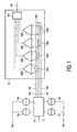
- Fig. 1 shows a circuit with a data communication connection.
- the circuit contains a driver 10 and a receiver 16 coupled via four signal conductors 14a-d.
- Driver 10 is supplied from four current sources 12a-d and has a signal input 11.
- Receiver 16 contains impedances 162a-d in the signal conductors 14a-d and four sense circuits 160a-d for sensing currents via signal conductors 14a-d, through voltage drops over impedances 162a-d.
- a decoder 164 is coupled to the outputs of the sense circuits. An output of the decoder is an output of receiver 16.
- Input 11 of driver 10 and output 166 of receiver 16 may be coupled to functional further circuits (not shown) which produce and use the signals transmitted via signal conductors 14a-d respectively.
- driver 10 supplies current from current sources 12a-d to signal conductors 14a-d.
- Driver 10 basically performs the function of a switch matrix, which determines which combinations of current sources 12a-d are connected to which signal conductors 14a-d, under the control of input signals supplied to input 11.
- a switch matrix which determines which combinations of current sources 12a-d are connected to which signal conductors 14a-d, under the control of input signals supplied to input 11.
- current combinations like (I,I,-I,-I), (2I,0,I,-I) etc and permutations thereof may be supplied to the signal conductors (the currents between a pair of brackets indicating currents to respective ones of the signal conductors 14a-d in a specific combination).
- Receiver 16 senses the currents through the various signal conductors and signals the sensed currents to decoder 164, which reconstructs the input signals and supplies reconstructed signals to output 166.
- the net sum of currents through signal conductors is zero at all times.
- no common impedance to ground need be connected to the common point 168 of the signal conductors (a high impedance bleeder resistance may be included to cope with inaccuracies).
- the important point, however, is that the net sum of the currents is constant. This makes it possible to communicate data symbols over signal conductors 14a-d at a high rate. If the sum is non-zero an impedance may be connected to the common point.
- Signal conductors 14a-d can be relatively long. To ensure that no significant signal distortion occurs it is desirable that there are little or no reflections over signal conductors 14a-d and that there is little or no cross-coupling, or at least that the cross-coupling is symmetrical in the sense that interchanging the currents of any two signal conductors does not significantly affect transmission properties.
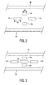
- Fig. 2 shows a cross section of signal conductors 14a-d in a plane perpendicular to the direction of propagation from driver 10 to receiver 16.
- Signal conductors 14a-d are included between conducting shield planes 20, 22 which extend in parallel to each other and to signal conductors 14a-d along most or all of the distance from driver 10 to receiver 16 in the direction perpendicular to the plane of cross-section that is shown in Fig. 2.
- Shield planes 20, 22 are electrically connected to each other, at least for signals in the frequency range used on signal conductors 14a-d. This may be realized for example by connecting both shield planes 20, 22 to ground or to a power supply connection Vdd or Vss.
- the region of the space between shield planes 20,22 that contains signal conductors 14a-d contains a non-conducting medium surrounding signal conductors 14a-d.
- the medium may be a conventional material used for printed circuit boards.
- the medium is preferably homogeneous between planes 20, 22 or stratified in layers parallel to the planes 20, 22.
- Two of the signal conductors 14b,c are stacked symmetrically in a perpendicular column between the planes 20, 22.
- the two other signal conductors 14a,d are provided midway between the planes, symmetrically on mutually opposite sides of the stack of signal conductors 14b,c.
- the width W2 of signal conductors 14b,c in the stack is smaller than the width W1 of conductors 14a,d on mutually opposite sides of the stack.
- Each of the signal conductors 14a-d forms a transmission line in combination with shield planes 20, 22.
- the transmission impedances of the transmission line formed by a signal conductor 14a-d depend on the distance between the signal conductors 14a-d and the shield planes 20, 22 and the width W1, W2 of the signal conductor 14a-d. For a given distance, the transmission impedance decreases as the width W1, W2 increases and for a given width W1, W2 the impedance decreases when the distance to the closest shield plane 20, 22 decreases.
- the same transmission impedance can be realized with a signal conductor 14b,c close to the shield planes as with a wider signals conductor 14a,d at a greater distance from shield planes 20, 22. This is used in the arrangement of Fig. 2 by choosing widths W1 and W2 so that each signal conductor 14a-d has the same transmission line impedance relative to shield planes 20, 22.
- the required width W1 or W2 can be determined experimentally for example by measuring the impedances individually and increasing or decreasing the widths of one pair of signal conductors 14a-d until matching of the impedances is realized.
- the impedance of a signal conductor 14a-d is a continuously decreasing function of its width: consequently it is always clear in which direction any width should be changed to reduce the difference in impedance.
- the impedance may be computed using a known computer program for solving Maxwell's equations.
- the impedances will also depend on the relative location of the various signal conductors 14a-d, the distance between planes 20, 22 and the material used for the medium surrounding the signal conductors. This makes it desirable to determine the required widths for each different design of the arrangement of signal conductors 14a-d separately.
- the distance between the signal conductors 14a-d is chosen to provide equal coupling strength between each pair of signal conductors 14a-d.
- the distance between the signal conductors 14b,c in the stack there are also three parameters of the structure that can be set: the distance between the signal conductors 14b,c in the stack, the distance between the signal conductors 14a,d on opposite sides of the stack and the widths W1, W2 which may be varied as long as the transmission line impedances of all signal conductors 14a-d vary in the same way. As a result, these distances and widths can be set so that all coupling strengths become substantially equal. As a further parameter to adjust the coupling strengths relative to one another, the distance between planes 20, 22 may be varied.
- Signal conductors 14a-d are not shown to scale. However, as shown, signal conductors 14a-d are preferably rectangular in shape, all having the same height.
- the required distances and impedances can be determined experimentally, by measuring impedances and cross coupling strength and adjusting the distances can be found by gradually increasing or decreasing the distances until the cross-coupling strengths and the impedances are found to be equal.
- each cross-coupling strength increases continuously as the distance between the relevant signal conductors 14a-d is reduced. Consequently, the direction of changes in distance that are required to reduce the difference can readily be determined.
- the cross coupling strengths will also depend on the relative location of the various signal conductors 14a-d, the distance between planes 20, 22 and the material used for the medium surrounding the signal conductors. This makes it desirable to determine the required distances and widths for each different design of the arrangement of signal conductors 14a-d separately.
- Fig. 3 shows a cross section of an arrangement of signal conductors 14a-d.
- a shield conductor 30 has been added, which is located in the stack of signal conductors 14b,c, midway between planes 20, 22.
- Shield conductor 30 is electrically connected to shield planes, at least for signals in the frequency range of the signals on signal conductors 14a-d.
- Shield conductor 30 serves to reduce the coupling strength between signal conductors 14a-d.
- shield conductor 30 is wider than the signal conductors 14c,d in the stack.
- the widths of signal conductors 14a-d are chosen so that substantially equal transmission impedances of the transmission lines formed by, on the one hand, shield planes 20, 22 and shield conductor 30 and, on the other hand, respective ones of the signal conductors 14a-d are realized.
- additional conductors may be added, for example shield conductors midway between planes 20, 22 on opposite sides of the arrangement of the four signal conductors 14a-d. Additional sets of four signal conductors may be added in parallel for transmitting more signals in parallel.
- the signal conductors 14a-d may be applied for example on printed circuit boards, or the substrate of a multi component module (MCM) to couple a driver 10 in one integrated circuit chip to a receiver in another integrated circuit chip, or in the packages of BGA ICs for proper signal transfer from the die to the PCB.
- MCM multi component module
Landscapes
- Engineering & Computer Science (AREA)
- Signal Processing (AREA)
- Computer Networks & Wireless Communication (AREA)
- Power Engineering (AREA)
- Microelectronics & Electronic Packaging (AREA)
- Dc Digital Transmission (AREA)
- Structure Of Printed Boards (AREA)
- Cable Transmission Systems, Equalization Of Radio And Reduction Of Echo (AREA)
- Near-Field Transmission Systems (AREA)
- Ladders (AREA)
Claims (4)
- Datenverarbeitungsschaltung, umfassend:- einen Treiber mit vier Signalausgängen;- einen Empfänger mit vier Eingängen;- einen ersten, zweiten, dritten und vierten Signalleiter, wobei jeder zwischen einem jeweiligen der Eingänge und Ausgänge in verbundener Weise angeordnet ist;- erste und zweite gegenseitig gekoppelte leitende Abschirmungsebenen, dadurch gekennzeichnet, dass die ersten und zweiten Signalleiter einen symmetrischen Stapel in einer Spalte zwischen der ersten und der zweiten Ebene bilden, die dritten und vierten Signalleiter im Wesentlichen in der Mitte zwischen der ersten und der zweiten Ebene auf gegenseitig entgegengesetzten Seiten des Stapels angeordnet sind, die ersten, zweiten, dritten und vierten Signalleiter jeweilige Breiten derart aufweisen, dass jeweilige Übertragungsleitungs-Impedanzen von Übertragungsleitungen zwischen jedem einzelnen der ersten, zweiten, dritten und vierten Signalleiter und der ersten und zweiten Ebenen im Wesentlichen gegenseitig gleich sind.
- Datenverarbeitungsschaltung nach Anspruch 1, die einen Abschirmungsleiter umfasst, der sich zwischen dem ersten und dem zweiten Signalleiter in der Mitte zwischen der ersten und der zweiten Ebene befindet.
- Datenverarbeitungsschaltung nach Anspruch 2, wobei sich der Abschirmungsleiter weiter in einer Richtung parallel zu der ersten und der zweiten Ebene und senkrecht zu einer Ausbreitungsrichtung erstreckt als der erste und der zweite der Leiter.
- Datenverarbeitungsschaltung nach Anspruch 1, wobei ein erster Abstand zwischen den ersten und zweiten Signalleitern im Stapel, ein zweiter Abstand zwischen den dritten und vierten Signalleitern und die Breiten der ersten, zweiten, dritten und vierten Signalleiter derart ausgewählt worden sind, dass es wesentliche Gleichheit zwischen einer ersten Kopplungsstärke zwischen den ersten und zweiten Signalleitern, einer zweiten Kopplungsstärke zwischen den dritten und vierten Signalleitern und einer dritten Kopplungsstärke zwischen den dritten oder vierten Signalleitern und dem ersten oder zweiten Signalleiter gibt.
Priority Applications (1)
| Application Number | Priority Date | Filing Date | Title |
|---|---|---|---|
| EP04705144A EP1590933B1 (de) | 2003-01-29 | 2004-01-26 | Leiteranordnung für eine übertragungsleitung |
Applications Claiming Priority (4)
| Application Number | Priority Date | Filing Date | Title |
|---|---|---|---|
| EP03100183 | 2003-01-29 | ||
| EP03100183 | 2003-01-29 | ||
| EP04705144A EP1590933B1 (de) | 2003-01-29 | 2004-01-26 | Leiteranordnung für eine übertragungsleitung |
| PCT/IB2004/050052 WO2004068812A2 (en) | 2003-01-29 | 2004-01-26 | Transmission line conductor arrangement |
Publications (2)
| Publication Number | Publication Date |
|---|---|
| EP1590933A2 EP1590933A2 (de) | 2005-11-02 |
| EP1590933B1 true EP1590933B1 (de) | 2006-11-22 |
Family
ID=32798990
Family Applications (1)
| Application Number | Title | Priority Date | Filing Date |
|---|---|---|---|
| EP04705144A Expired - Lifetime EP1590933B1 (de) | 2003-01-29 | 2004-01-26 | Leiteranordnung für eine übertragungsleitung |
Country Status (8)
| Country | Link |
|---|---|
| US (1) | US7535963B2 (de) |
| EP (1) | EP1590933B1 (de) |
| JP (1) | JP2006516860A (de) |
| KR (1) | KR20050103480A (de) |
| CN (1) | CN100525265C (de) |
| AT (1) | ATE346443T1 (de) |
| DE (1) | DE602004003337T2 (de) |
| WO (1) | WO2004068812A2 (de) |
Families Citing this family (4)
| Publication number | Priority date | Publication date | Assignee | Title |
|---|---|---|---|---|
| RU2369977C2 (ru) * | 2005-03-23 | 2009-10-10 | Квэлкомм Инкорпорейтед | Устройство сопряжения токового режима для высокоскоростной связи вне микросхем |
| DE102010039716B4 (de) * | 2010-08-24 | 2012-09-20 | Gcd Hard- & Software Gmbh | Verfahren zur Übertragung eines Nutzsignals |
| CN102802339B (zh) * | 2011-05-23 | 2017-05-24 | 永捷电子(始兴)有限公司 | 印刷电路板 |
| CN114357934A (zh) * | 2021-12-29 | 2022-04-15 | 海光信息技术股份有限公司 | 电路布线方法及电路 |
Family Cites Families (7)
| Publication number | Priority date | Publication date | Assignee | Title |
|---|---|---|---|---|
| US5412689A (en) * | 1992-12-23 | 1995-05-02 | International Business Machines Corporation | Modal propagation of information through a defined transmission medium |
| US6005895A (en) * | 1996-12-20 | 1999-12-21 | Rambus Inc. | Apparatus and method for multilevel signaling |
| US6556628B1 (en) * | 1999-04-29 | 2003-04-29 | The University Of North Carolina At Chapel Hill | Methods and systems for transmitting and receiving differential signals over a plurality of conductors |
| US6486405B2 (en) * | 2000-12-01 | 2002-11-26 | Hon Hai Precision Ind. Co., Ltd. | Arrangement of differential pair for eliminating crosstalk in high speed application |
| US6987822B2 (en) * | 2001-03-13 | 2006-01-17 | Micron Technology, Inc. | Circuit and method for reducing noise interference in digital differential input receivers |
| US6444902B1 (en) * | 2001-04-10 | 2002-09-03 | Hon Hai Precision Ind. Co., Ltd. | Electrical cable |
| JP2004254155A (ja) * | 2003-02-21 | 2004-09-09 | Kanji Otsuka | 信号伝送装置および配線構造 |
-
2004
- 2004-01-26 EP EP04705144A patent/EP1590933B1/de not_active Expired - Lifetime
- 2004-01-26 US US10/543,433 patent/US7535963B2/en not_active Expired - Fee Related
- 2004-01-26 CN CNB2004800029517A patent/CN100525265C/zh not_active Expired - Fee Related
- 2004-01-26 AT AT04705144T patent/ATE346443T1/de not_active IP Right Cessation
- 2004-01-26 DE DE602004003337T patent/DE602004003337T2/de not_active Expired - Lifetime
- 2004-01-26 KR KR1020057013902A patent/KR20050103480A/ko not_active Abandoned
- 2004-01-26 WO PCT/IB2004/050052 patent/WO2004068812A2/en not_active Ceased
- 2004-01-26 JP JP2006502542A patent/JP2006516860A/ja active Pending
Also Published As
| Publication number | Publication date |
|---|---|
| JP2006516860A (ja) | 2006-07-06 |
| DE602004003337D1 (de) | 2007-01-04 |
| US20060140283A1 (en) | 2006-06-29 |
| EP1590933A2 (de) | 2005-11-02 |
| WO2004068812A2 (en) | 2004-08-12 |
| US7535963B2 (en) | 2009-05-19 |
| WO2004068812A3 (en) | 2004-09-16 |
| ATE346443T1 (de) | 2006-12-15 |
| KR20050103480A (ko) | 2005-10-31 |
| CN100525265C (zh) | 2009-08-05 |
| CN1742470A (zh) | 2006-03-01 |
| DE602004003337T2 (de) | 2007-06-21 |
Similar Documents
| Publication | Publication Date | Title |
|---|---|---|
| EP1629391B1 (de) | Kompakter elektromagnetischer koppler zur verwendung mit digitalen übertragungssystemen | |
| CN104051425B (zh) | 用于减少通道串扰的耦合通孔 | |
| US6420778B1 (en) | Differential electrical transmission line structures employing crosstalk compensation and related methods | |
| US6359931B1 (en) | Apparatus and method for multilevel signaling | |
| US5365205A (en) | Backplane databus utilizing directional couplers | |
| US7038555B2 (en) | Printed wiring board for controlling signal transmission using paired inductance and capacitance | |
| US8609996B2 (en) | Printed circuit board and layout method thereof | |
| US20110007487A1 (en) | Lsi package, printed board and electronic device | |
| CN102142420A (zh) | 互连结构 | |
| CN100555850C (zh) | 用于数字器件互连的装置、方法和网络 | |
| US7535963B2 (en) | Data processing circuit with a driver and a receiver | |
| US7371966B2 (en) | High speed active flex cable link | |
| US20030128079A1 (en) | Digital network | |
| US20040103383A1 (en) | Design, layout and method of manufacture for a circuit that taps a differential signal | |
| KR20190088523A (ko) | 비아-리스 빔 형성기를 위한 회로 및 기법 | |
| CN101686068B (zh) | 一种功分网络装置 | |
| US7292449B2 (en) | Virtual ground return for reduction of radiated emissions | |
| US20070093080A1 (en) | Pin contact with direct in-line connection to equalization component | |
| TW201141332A (en) | Printed circuit board and layout method thereof | |
| US20250175368A1 (en) | Scalable routing topologies that enable increased loads on single-ended or differential channels | |
| US20230209726A1 (en) | Printed circuit board having a differential pair routing topology with negative plane routing and impedance correction structures | |
| Chi et al. | A low cost dual-CPW differential line for two layer PCBs | |
| JPH04181416A (ja) | ラジアル・バス | |
| HK1235150A1 (en) | Semiconductor device | |
| TWM379261U (en) | Electrical connector with crosstalk compensation |
Legal Events
| Date | Code | Title | Description |
|---|---|---|---|
| PUAI | Public reference made under article 153(3) epc to a published international application that has entered the european phase |
Free format text: ORIGINAL CODE: 0009012 |
|
| 17P | Request for examination filed |
Effective date: 20050829 |
|
| AK | Designated contracting states |
Kind code of ref document: A2 Designated state(s): AT BE BG CH CY CZ DE DK EE ES FI FR GB GR HU IE IT LI LU MC NL PT RO SE SI SK TR |
|
| AX | Request for extension of the european patent |
Extension state: AL LT LV MK |
|
| GRAP | Despatch of communication of intention to grant a patent |
Free format text: ORIGINAL CODE: EPIDOSNIGR1 |
|
| DAX | Request for extension of the european patent (deleted) | ||
| GRAS | Grant fee paid |
Free format text: ORIGINAL CODE: EPIDOSNIGR3 |
|
| GRAA | (expected) grant |
Free format text: ORIGINAL CODE: 0009210 |
|
| AK | Designated contracting states |
Kind code of ref document: B1 Designated state(s): AT BE BG CH CY CZ DE DK EE ES FI FR GB GR HU IE IT LI LU MC NL PT RO SE SI SK TR |
|
| PG25 | Lapsed in a contracting state [announced via postgrant information from national office to epo] |
Ref country code: SK Free format text: LAPSE BECAUSE OF FAILURE TO SUBMIT A TRANSLATION OF THE DESCRIPTION OR TO PAY THE FEE WITHIN THE PRESCRIBED TIME-LIMIT Effective date: 20061122 Ref country code: SI Free format text: LAPSE BECAUSE OF FAILURE TO SUBMIT A TRANSLATION OF THE DESCRIPTION OR TO PAY THE FEE WITHIN THE PRESCRIBED TIME-LIMIT Effective date: 20061122 Ref country code: RO Free format text: LAPSE BECAUSE OF FAILURE TO SUBMIT A TRANSLATION OF THE DESCRIPTION OR TO PAY THE FEE WITHIN THE PRESCRIBED TIME-LIMIT Effective date: 20061122 Ref country code: NL Free format text: LAPSE BECAUSE OF FAILURE TO SUBMIT A TRANSLATION OF THE DESCRIPTION OR TO PAY THE FEE WITHIN THE PRESCRIBED TIME-LIMIT Effective date: 20061122 Ref country code: LI Free format text: LAPSE BECAUSE OF FAILURE TO SUBMIT A TRANSLATION OF THE DESCRIPTION OR TO PAY THE FEE WITHIN THE PRESCRIBED TIME-LIMIT Effective date: 20061122 Ref country code: IT Free format text: LAPSE BECAUSE OF FAILURE TO SUBMIT A TRANSLATION OF THE DESCRIPTION OR TO PAY THE FEE WITHIN THE PRESCRIBED TIME-LIMIT;WARNING: LAPSES OF ITALIAN PATENTS WITH EFFECTIVE DATE BEFORE 2007 MAY HAVE OCCURRED AT ANY TIME BEFORE 2007. THE CORRECT EFFECTIVE DATE MAY BE DIFFERENT FROM THE ONE RECORDED. Effective date: 20061122 Ref country code: FI Free format text: LAPSE BECAUSE OF FAILURE TO SUBMIT A TRANSLATION OF THE DESCRIPTION OR TO PAY THE FEE WITHIN THE PRESCRIBED TIME-LIMIT Effective date: 20061122 Ref country code: CZ Free format text: LAPSE BECAUSE OF FAILURE TO SUBMIT A TRANSLATION OF THE DESCRIPTION OR TO PAY THE FEE WITHIN THE PRESCRIBED TIME-LIMIT Effective date: 20061122 Ref country code: CH Free format text: LAPSE BECAUSE OF FAILURE TO SUBMIT A TRANSLATION OF THE DESCRIPTION OR TO PAY THE FEE WITHIN THE PRESCRIBED TIME-LIMIT Effective date: 20061122 Ref country code: BE Free format text: LAPSE BECAUSE OF FAILURE TO SUBMIT A TRANSLATION OF THE DESCRIPTION OR TO PAY THE FEE WITHIN THE PRESCRIBED TIME-LIMIT Effective date: 20061122 Ref country code: AT Free format text: LAPSE BECAUSE OF FAILURE TO SUBMIT A TRANSLATION OF THE DESCRIPTION OR TO PAY THE FEE WITHIN THE PRESCRIBED TIME-LIMIT Effective date: 20061122 |
|
| REG | Reference to a national code |
Ref country code: GB Ref legal event code: FG4D |
|
| REG | Reference to a national code |
Ref country code: CH Ref legal event code: EP |
|
| REG | Reference to a national code |
Ref country code: IE Ref legal event code: FG4D |
|
| REF | Corresponds to: |
Ref document number: 602004003337 Country of ref document: DE Date of ref document: 20070104 Kind code of ref document: P |
|
| PG25 | Lapsed in a contracting state [announced via postgrant information from national office to epo] |
Ref country code: IE Free format text: LAPSE BECAUSE OF NON-PAYMENT OF DUE FEES Effective date: 20070126 |
|
| PG25 | Lapsed in a contracting state [announced via postgrant information from national office to epo] |
Ref country code: MC Free format text: LAPSE BECAUSE OF NON-PAYMENT OF DUE FEES Effective date: 20070131 |
|
| PG25 | Lapsed in a contracting state [announced via postgrant information from national office to epo] |
Ref country code: SE Free format text: LAPSE BECAUSE OF FAILURE TO SUBMIT A TRANSLATION OF THE DESCRIPTION OR TO PAY THE FEE WITHIN THE PRESCRIBED TIME-LIMIT Effective date: 20070222 Ref country code: DK Free format text: LAPSE BECAUSE OF FAILURE TO SUBMIT A TRANSLATION OF THE DESCRIPTION OR TO PAY THE FEE WITHIN THE PRESCRIBED TIME-LIMIT Effective date: 20070222 Ref country code: BG Free format text: LAPSE BECAUSE OF FAILURE TO SUBMIT A TRANSLATION OF THE DESCRIPTION OR TO PAY THE FEE WITHIN THE PRESCRIBED TIME-LIMIT Effective date: 20070222 |
|
| PG25 | Lapsed in a contracting state [announced via postgrant information from national office to epo] |
Ref country code: ES Free format text: LAPSE BECAUSE OF FAILURE TO SUBMIT A TRANSLATION OF THE DESCRIPTION OR TO PAY THE FEE WITHIN THE PRESCRIBED TIME-LIMIT Effective date: 20070305 |
|
| PG25 | Lapsed in a contracting state [announced via postgrant information from national office to epo] |
Ref country code: PT Free format text: LAPSE BECAUSE OF FAILURE TO SUBMIT A TRANSLATION OF THE DESCRIPTION OR TO PAY THE FEE WITHIN THE PRESCRIBED TIME-LIMIT Effective date: 20070423 |
|
| NLV1 | Nl: lapsed or annulled due to failure to fulfill the requirements of art. 29p and 29m of the patents act | ||
| ET | Fr: translation filed | ||
| REG | Reference to a national code |
Ref country code: CH Ref legal event code: PL |
|
| PLBE | No opposition filed within time limit |
Free format text: ORIGINAL CODE: 0009261 |
|
| STAA | Information on the status of an ep patent application or granted ep patent |
Free format text: STATUS: NO OPPOSITION FILED WITHIN TIME LIMIT |
|
| 26N | No opposition filed |
Effective date: 20070823 |
|
| PG25 | Lapsed in a contracting state [announced via postgrant information from national office to epo] |
Ref country code: GR Free format text: LAPSE BECAUSE OF FAILURE TO SUBMIT A TRANSLATION OF THE DESCRIPTION OR TO PAY THE FEE WITHIN THE PRESCRIBED TIME-LIMIT Effective date: 20070223 |
|
| REG | Reference to a national code |
Ref country code: GB Ref legal event code: 732E |
|
| PG25 | Lapsed in a contracting state [announced via postgrant information from national office to epo] |
Ref country code: EE Free format text: LAPSE BECAUSE OF FAILURE TO SUBMIT A TRANSLATION OF THE DESCRIPTION OR TO PAY THE FEE WITHIN THE PRESCRIBED TIME-LIMIT Effective date: 20061122 |
|
| REG | Reference to a national code |
Ref country code: FR Ref legal event code: TP |
|
| PG25 | Lapsed in a contracting state [announced via postgrant information from national office to epo] |
Ref country code: LU Free format text: LAPSE BECAUSE OF NON-PAYMENT OF DUE FEES Effective date: 20070126 Ref country code: CY Free format text: LAPSE BECAUSE OF FAILURE TO SUBMIT A TRANSLATION OF THE DESCRIPTION OR TO PAY THE FEE WITHIN THE PRESCRIBED TIME-LIMIT Effective date: 20061122 |
|
| PG25 | Lapsed in a contracting state [announced via postgrant information from national office to epo] |
Ref country code: TR Free format text: LAPSE BECAUSE OF FAILURE TO SUBMIT A TRANSLATION OF THE DESCRIPTION OR TO PAY THE FEE WITHIN THE PRESCRIBED TIME-LIMIT Effective date: 20061122 Ref country code: HU Free format text: LAPSE BECAUSE OF FAILURE TO SUBMIT A TRANSLATION OF THE DESCRIPTION OR TO PAY THE FEE WITHIN THE PRESCRIBED TIME-LIMIT Effective date: 20070523 |
|
| PGFP | Annual fee paid to national office [announced via postgrant information from national office to epo] |
Ref country code: GB Payment date: 20121224 Year of fee payment: 10 |
|
| GBPC | Gb: european patent ceased through non-payment of renewal fee |
Effective date: 20140126 |
|
| PG25 | Lapsed in a contracting state [announced via postgrant information from national office to epo] |
Ref country code: GB Free format text: LAPSE BECAUSE OF NON-PAYMENT OF DUE FEES Effective date: 20140126 |
|
| REG | Reference to a national code |
Ref country code: FR Ref legal event code: PLFP Year of fee payment: 12 |
|
| REG | Reference to a national code |
Ref country code: FR Ref legal event code: PLFP Year of fee payment: 13 |
|
| REG | Reference to a national code |
Ref country code: FR Ref legal event code: PLFP Year of fee payment: 14 |
|
| REG | Reference to a national code |
Ref country code: FR Ref legal event code: PLFP Year of fee payment: 15 |
|
| PGFP | Annual fee paid to national office [announced via postgrant information from national office to epo] |
Ref country code: FR Payment date: 20191219 Year of fee payment: 17 |
|
| PGFP | Annual fee paid to national office [announced via postgrant information from national office to epo] |
Ref country code: DE Payment date: 20191218 Year of fee payment: 17 |
|
| REG | Reference to a national code |
Ref country code: DE Ref legal event code: R119 Ref document number: 602004003337 Country of ref document: DE |
|
| PG25 | Lapsed in a contracting state [announced via postgrant information from national office to epo] |
Ref country code: FR Free format text: LAPSE BECAUSE OF NON-PAYMENT OF DUE FEES Effective date: 20210131 |
|
| PG25 | Lapsed in a contracting state [announced via postgrant information from national office to epo] |
Ref country code: DE Free format text: LAPSE BECAUSE OF NON-PAYMENT OF DUE FEES Effective date: 20210803 |