EP1591777B1 - Capteur d'hydrogène et procédé de détection d'hydrogène - Google Patents
Capteur d'hydrogène et procédé de détection d'hydrogène Download PDFInfo
- Publication number
- EP1591777B1 EP1591777B1 EP05009229.5A EP05009229A EP1591777B1 EP 1591777 B1 EP1591777 B1 EP 1591777B1 EP 05009229 A EP05009229 A EP 05009229A EP 1591777 B1 EP1591777 B1 EP 1591777B1
- Authority
- EP
- European Patent Office
- Prior art keywords
- hydrogen
- semiconductor
- absorber
- gas
- resistance
- Prior art date
- Legal status (The legal status is an assumption and is not a legal conclusion. Google has not performed a legal analysis and makes no representation as to the accuracy of the status listed.)
- Expired - Lifetime
Links
- 239000001257 hydrogen Substances 0.000 title claims description 279
- 229910052739 hydrogen Inorganic materials 0.000 title claims description 279
- UFHFLCQGNIYNRP-UHFFFAOYSA-N Hydrogen Chemical compound [H][H] UFHFLCQGNIYNRP-UHFFFAOYSA-N 0.000 title claims description 205
- 150000002431 hydrogen Chemical class 0.000 title claims description 115
- 238000000034 method Methods 0.000 title claims description 17
- 239000004065 semiconductor Substances 0.000 claims description 134
- 239000006096 absorbing agent Substances 0.000 claims description 87
- 239000010408 film Substances 0.000 claims description 58
- 230000008859 change Effects 0.000 claims description 37
- 238000001514 detection method Methods 0.000 claims description 35
- 239000000758 substrate Substances 0.000 claims description 27
- KDLHZDBZIXYQEI-UHFFFAOYSA-N Palladium Chemical compound [Pd] KDLHZDBZIXYQEI-UHFFFAOYSA-N 0.000 claims description 22
- 239000002245 particle Substances 0.000 claims description 19
- 239000010409 thin film Substances 0.000 claims description 13
- 229910002601 GaN Inorganic materials 0.000 claims description 10
- JMASRVWKEDWRBT-UHFFFAOYSA-N Gallium nitride Chemical compound [Ga]#N JMASRVWKEDWRBT-UHFFFAOYSA-N 0.000 claims description 10
- BASFCYQUMIYNBI-UHFFFAOYSA-N platinum Chemical compound [Pt] BASFCYQUMIYNBI-UHFFFAOYSA-N 0.000 claims description 9
- 238000010521 absorption reaction Methods 0.000 claims description 8
- VYPSYNLAJGMNEJ-UHFFFAOYSA-N Silicium dioxide Chemical compound O=[Si]=O VYPSYNLAJGMNEJ-UHFFFAOYSA-N 0.000 claims description 7
- XUIMIQQOPSSXEZ-UHFFFAOYSA-N Silicon Chemical compound [Si] XUIMIQQOPSSXEZ-UHFFFAOYSA-N 0.000 claims description 7
- 229910052710 silicon Inorganic materials 0.000 claims description 7
- 239000010703 silicon Substances 0.000 claims description 7
- JBRZTFJDHDCESZ-UHFFFAOYSA-N AsGa Chemical compound [As]#[Ga] JBRZTFJDHDCESZ-UHFFFAOYSA-N 0.000 claims description 4
- 229910001218 Gallium arsenide Inorganic materials 0.000 claims description 4
- 229910000577 Silicon-germanium Inorganic materials 0.000 claims description 4
- 239000012466 permeate Substances 0.000 claims description 4
- HBMJWWWQQXIZIP-UHFFFAOYSA-N silicon carbide Chemical compound [Si+]#[C-] HBMJWWWQQXIZIP-UHFFFAOYSA-N 0.000 claims description 4
- 229910010271 silicon carbide Inorganic materials 0.000 claims description 4
- 229910001252 Pd alloy Inorganic materials 0.000 claims description 3
- 229910001260 Pt alloy Inorganic materials 0.000 claims description 3
- 229910052581 Si3N4 Inorganic materials 0.000 claims description 3
- 229910052763 palladium Inorganic materials 0.000 claims description 3
- 239000004642 Polyimide Substances 0.000 claims description 2
- LEVVHYCKPQWKOP-UHFFFAOYSA-N [Si].[Ge] Chemical compound [Si].[Ge] LEVVHYCKPQWKOP-UHFFFAOYSA-N 0.000 claims description 2
- 239000010432 diamond Substances 0.000 claims description 2
- 229910003460 diamond Inorganic materials 0.000 claims description 2
- 229910052732 germanium Inorganic materials 0.000 claims description 2
- GNPVGFCGXDBREM-UHFFFAOYSA-N germanium atom Chemical compound [Ge] GNPVGFCGXDBREM-UHFFFAOYSA-N 0.000 claims description 2
- 229910052697 platinum Inorganic materials 0.000 claims description 2
- 229920001721 polyimide Polymers 0.000 claims description 2
- HQVNEWCFYHHQES-UHFFFAOYSA-N silicon nitride Chemical compound N12[Si]34N5[Si]62N3[Si]51N64 HQVNEWCFYHHQES-UHFFFAOYSA-N 0.000 claims description 2
- 229910052814 silicon oxide Inorganic materials 0.000 claims description 2
- 239000007789 gas Substances 0.000 description 76
- IJGRMHOSHXDMSA-UHFFFAOYSA-N Atomic nitrogen Chemical compound N#N IJGRMHOSHXDMSA-UHFFFAOYSA-N 0.000 description 19
- 229910001873 dinitrogen Inorganic materials 0.000 description 19
- 238000010438 heat treatment Methods 0.000 description 16
- ATUOYWHBWRKTHZ-UHFFFAOYSA-N Propane Chemical compound CCC ATUOYWHBWRKTHZ-UHFFFAOYSA-N 0.000 description 15
- 239000000463 material Substances 0.000 description 15
- 239000001301 oxygen Substances 0.000 description 15
- 229910052760 oxygen Inorganic materials 0.000 description 15
- QVGXLLKOCUKJST-UHFFFAOYSA-N atomic oxygen Chemical compound [O] QVGXLLKOCUKJST-UHFFFAOYSA-N 0.000 description 14
- 230000003247 decreasing effect Effects 0.000 description 14
- 238000005259 measurement Methods 0.000 description 14
- VNWKTOKETHGBQD-UHFFFAOYSA-N methane Chemical compound C VNWKTOKETHGBQD-UHFFFAOYSA-N 0.000 description 14
- LFQSCWFLJHTTHZ-UHFFFAOYSA-N Ethanol Chemical compound CCO LFQSCWFLJHTTHZ-UHFFFAOYSA-N 0.000 description 12
- 239000003054 catalyst Substances 0.000 description 9
- 238000006243 chemical reaction Methods 0.000 description 9
- 230000007246 mechanism Effects 0.000 description 8
- CURLTUGMZLYLDI-UHFFFAOYSA-N Carbon dioxide Chemical compound O=C=O CURLTUGMZLYLDI-UHFFFAOYSA-N 0.000 description 7
- 239000003795 chemical substances by application Substances 0.000 description 7
- 238000009434 installation Methods 0.000 description 7
- 230000003647 oxidation Effects 0.000 description 7
- 238000007254 oxidation reaction Methods 0.000 description 7
- 231100000572 poisoning Toxicity 0.000 description 7
- 230000000607 poisoning effect Effects 0.000 description 7
- 239000001294 propane Substances 0.000 description 7
- 229910002091 carbon monoxide Inorganic materials 0.000 description 6
- PJXISJQVUVHSOJ-UHFFFAOYSA-N indium(III) oxide Inorganic materials [O-2].[O-2].[O-2].[In+3].[In+3] PJXISJQVUVHSOJ-UHFFFAOYSA-N 0.000 description 6
- NNPPMTNAJDCUHE-UHFFFAOYSA-N isobutane Chemical compound CC(C)C NNPPMTNAJDCUHE-UHFFFAOYSA-N 0.000 description 6
- 230000003252 repetitive effect Effects 0.000 description 6
- 230000035945 sensitivity Effects 0.000 description 6
- 235000019441 ethanol Nutrition 0.000 description 5
- 229910045601 alloy Inorganic materials 0.000 description 4
- 239000000956 alloy Substances 0.000 description 4
- 229910002092 carbon dioxide Inorganic materials 0.000 description 4
- -1 electrode Substances 0.000 description 4
- 150000002500 ions Chemical class 0.000 description 4
- 229910052751 metal Inorganic materials 0.000 description 4
- 239000002184 metal Substances 0.000 description 4
- 238000004544 sputter deposition Methods 0.000 description 4
- UGFAIRIUMAVXCW-UHFFFAOYSA-N Carbon monoxide Chemical compound [O+]#[C-] UGFAIRIUMAVXCW-UHFFFAOYSA-N 0.000 description 3
- 239000011358 absorbing material Substances 0.000 description 3
- 230000015572 biosynthetic process Effects 0.000 description 3
- 239000001569 carbon dioxide Substances 0.000 description 3
- 239000000919 ceramic Substances 0.000 description 3
- 230000008030 elimination Effects 0.000 description 3
- 238000003379 elimination reaction Methods 0.000 description 3
- 239000011521 glass Substances 0.000 description 3
- 239000001282 iso-butane Substances 0.000 description 3
- 230000001681 protective effect Effects 0.000 description 3
- 238000012360 testing method Methods 0.000 description 3
- 238000001771 vacuum deposition Methods 0.000 description 3
- GWEVSGVZZGPLCZ-UHFFFAOYSA-N Titan oxide Chemical compound O=[Ti]=O GWEVSGVZZGPLCZ-UHFFFAOYSA-N 0.000 description 2
- PNEYBMLMFCGWSK-UHFFFAOYSA-N aluminium oxide Inorganic materials [O-2].[O-2].[O-2].[Al+3].[Al+3] PNEYBMLMFCGWSK-UHFFFAOYSA-N 0.000 description 2
- 239000000969 carrier Substances 0.000 description 2
- 230000003197 catalytic effect Effects 0.000 description 2
- 229910052681 coesite Inorganic materials 0.000 description 2
- 230000000052 comparative effect Effects 0.000 description 2
- 229910052593 corundum Inorganic materials 0.000 description 2
- 229910052906 cristobalite Inorganic materials 0.000 description 2
- AMGQUBHHOARCQH-UHFFFAOYSA-N indium;oxotin Chemical compound [In].[Sn]=O AMGQUBHHOARCQH-UHFFFAOYSA-N 0.000 description 2
- 239000011810 insulating material Substances 0.000 description 2
- 229910044991 metal oxide Inorganic materials 0.000 description 2
- 150000004706 metal oxides Chemical class 0.000 description 2
- 238000006479 redox reaction Methods 0.000 description 2
- 238000006722 reduction reaction Methods 0.000 description 2
- 239000000377 silicon dioxide Substances 0.000 description 2
- 229910052682 stishovite Inorganic materials 0.000 description 2
- 229910052905 tridymite Inorganic materials 0.000 description 2
- 229910001845 yogo sapphire Inorganic materials 0.000 description 2
- QGZKDVFQNNGYKY-UHFFFAOYSA-O Ammonium Chemical compound [NH4+] QGZKDVFQNNGYKY-UHFFFAOYSA-O 0.000 description 1
- MYMOFIZGZYHOMD-UHFFFAOYSA-N Dioxygen Chemical compound O=O MYMOFIZGZYHOMD-UHFFFAOYSA-N 0.000 description 1
- XLOMVQKBTHCTTD-UHFFFAOYSA-N Zinc monoxide Chemical compound [Zn]=O XLOMVQKBTHCTTD-UHFFFAOYSA-N 0.000 description 1
- 229910052782 aluminium Inorganic materials 0.000 description 1
- 229910052785 arsenic Inorganic materials 0.000 description 1
- 239000012298 atmosphere Substances 0.000 description 1
- 239000002800 charge carrier Substances 0.000 description 1
- 239000004020 conductor Substances 0.000 description 1
- 239000000470 constituent Substances 0.000 description 1
- BERDEBHAJNAUOM-UHFFFAOYSA-N copper(I) oxide Inorganic materials [Cu]O[Cu] BERDEBHAJNAUOM-UHFFFAOYSA-N 0.000 description 1
- KRFJLUBVMFXRPN-UHFFFAOYSA-N cuprous oxide Chemical compound [O-2].[Cu+].[Cu+] KRFJLUBVMFXRPN-UHFFFAOYSA-N 0.000 description 1
- 230000001419 dependent effect Effects 0.000 description 1
- 238000000151 deposition Methods 0.000 description 1
- 230000008021 deposition Effects 0.000 description 1
- 229910001882 dioxygen Inorganic materials 0.000 description 1
- 230000000694 effects Effects 0.000 description 1
- 230000005611 electricity Effects 0.000 description 1
- 239000012776 electronic material Substances 0.000 description 1
- 238000011156 evaluation Methods 0.000 description 1
- 230000006870 function Effects 0.000 description 1
- 229910052737 gold Inorganic materials 0.000 description 1
- 230000006872 improvement Effects 0.000 description 1
- 239000011261 inert gas Substances 0.000 description 1
- 238000011835 investigation Methods 0.000 description 1
- 229910052746 lanthanum Inorganic materials 0.000 description 1
- 229910052749 magnesium Inorganic materials 0.000 description 1
- 239000007769 metal material Substances 0.000 description 1
- 150000002739 metals Chemical class 0.000 description 1
- 239000002105 nanoparticle Substances 0.000 description 1
- 229910000510 noble metal Inorganic materials 0.000 description 1
- 230000002093 peripheral effect Effects 0.000 description 1
- 229910052698 phosphorus Inorganic materials 0.000 description 1
- 238000000206 photolithography Methods 0.000 description 1
- 230000009993 protective function Effects 0.000 description 1
- 239000010453 quartz Substances 0.000 description 1
- 229910052761 rare earth metal Inorganic materials 0.000 description 1
- 150000002910 rare earth metals Chemical class 0.000 description 1
- 238000010405 reoxidation reaction Methods 0.000 description 1
- 230000027756 respiratory electron transport chain Effects 0.000 description 1
- 238000007650 screen-printing Methods 0.000 description 1
- 238000001179 sorption measurement Methods 0.000 description 1
- 229910052719 titanium Inorganic materials 0.000 description 1
- XLYOFNOQVPJJNP-UHFFFAOYSA-N water Substances O XLYOFNOQVPJJNP-UHFFFAOYSA-N 0.000 description 1
- 229910052726 zirconium Inorganic materials 0.000 description 1
Images


Classifications
-
- G—PHYSICS
- G01—MEASURING; TESTING
- G01N—INVESTIGATING OR ANALYSING MATERIALS BY DETERMINING THEIR CHEMICAL OR PHYSICAL PROPERTIES
- G01N27/00—Investigating or analysing materials by the use of electric, electrochemical, or magnetic means
- G01N27/02—Investigating or analysing materials by the use of electric, electrochemical, or magnetic means by investigating impedance
- G01N27/04—Investigating or analysing materials by the use of electric, electrochemical, or magnetic means by investigating impedance by investigating resistance
- G01N27/12—Investigating or analysing materials by the use of electric, electrochemical, or magnetic means by investigating impedance by investigating resistance of a solid body in dependence upon absorption of a fluid; of a solid body in dependence upon reaction with a fluid, for detecting components in the fluid
- G01N27/125—Composition of the body, e.g. the composition of its sensitive layer
-
- G—PHYSICS
- G01—MEASURING; TESTING
- G01N—INVESTIGATING OR ANALYSING MATERIALS BY DETERMINING THEIR CHEMICAL OR PHYSICAL PROPERTIES
- G01N33/00—Investigating or analysing materials by specific methods not covered by groups G01N1/00 - G01N31/00
- G01N33/0004—Gaseous mixtures, e.g. polluted air
- G01N33/0009—General constructional details of gas analysers, e.g. portable test equipment
- G01N33/0027—General constructional details of gas analysers, e.g. portable test equipment concerning the detector
- G01N33/0036—General constructional details of gas analysers, e.g. portable test equipment concerning the detector specially adapted to detect a particular component
- G01N33/005—H2
-
- Y—GENERAL TAGGING OF NEW TECHNOLOGICAL DEVELOPMENTS; GENERAL TAGGING OF CROSS-SECTIONAL TECHNOLOGIES SPANNING OVER SEVERAL SECTIONS OF THE IPC; TECHNICAL SUBJECTS COVERED BY FORMER USPC CROSS-REFERENCE ART COLLECTIONS [XRACs] AND DIGESTS
- Y10—TECHNICAL SUBJECTS COVERED BY FORMER USPC
- Y10S—TECHNICAL SUBJECTS COVERED BY FORMER USPC CROSS-REFERENCE ART COLLECTIONS [XRACs] AND DIGESTS
- Y10S436/00—Chemistry: analytical and immunological testing
- Y10S436/806—Electrical property or magnetic property
-
- Y—GENERAL TAGGING OF NEW TECHNOLOGICAL DEVELOPMENTS; GENERAL TAGGING OF CROSS-SECTIONAL TECHNOLOGIES SPANNING OVER SEVERAL SECTIONS OF THE IPC; TECHNICAL SUBJECTS COVERED BY FORMER USPC CROSS-REFERENCE ART COLLECTIONS [XRACs] AND DIGESTS
- Y10—TECHNICAL SUBJECTS COVERED BY FORMER USPC
- Y10T—TECHNICAL SUBJECTS COVERED BY FORMER US CLASSIFICATION
- Y10T436/00—Chemistry: analytical and immunological testing
- Y10T436/22—Hydrogen, per se
Definitions
- the present invention relates to a hydrogen sensor and a method for detecting hydrogen, the hydrogen sensor being able to simply detect hydrogen at room temperature and to detect only hydrogen without receiving any influence from the presence of flammable gases such as a methane gas and an alcohol.
- gas detection elements using metal oxide semiconductors such as SnO 2 and In 2 O 3 as a gas sensitive member have been known, and among the gas detection elements of this type, as an element which is devised so as to selectively detect a H 2 gas, for example, a hydrogen gas detection element described in Japanese Unexamined Patent Application Publication No. 3-259736 has been known.
- the hydrogen gas detection element disclosed in Japanese Unexamined Patent Application Publication No. 3-259736 has the structure in which an insulating substrate, an Sn oxide layer, comb-shaped electrodes, and a catalytic layer made of palladium are sequentially provided in that order on a heating element.
- a final step of forming the above element by performing heat treatment, besides improvement in sensitivity to a H 2 gas, the sensitivity to gases other than a H2 gas is decreased.
- the hydrogen gas detection element described above has the structure in which comb-shaped Au electrodes are formed on a semiconductive Sn oxide film (SnO 2 ), and on the films mentioned above, a catalytic layer of Pd (palladium) or Pt (platinum) formed by vacuum deposition and having a mass film thickness of approximately 1 to 5 nm is provided.
- the hydrogen gas detection element described above responds to an ethanol gas (C 2 H 5 OH), a propane gas (C 3 H 8 ), and a carbon monoxide gas (CO) besides a hydrogen gas.
- a hydrogen sensor having a different structure from the above structure for example, the structure has been proposed in which on a surface of a gas sensitive member made of a metal oxide semiconductor such as SnO 2 or In 2 O 3 , a thin film made of a non-flammable material such as Al 2 O 3 , SiO 2 , or Si 3 N 4 , is formed, the thin film preventing molecules other than hydrogen from permeating therethrough and easily permitting hydrogen molecules to permeate.
- a hydrogen sensor having the structure described above aims to realize a highly sensitive hydrogen selective sensor by forming a dense, uniform, continuous thin film (hydrogen selective permeable film) on a surface of a gas sensitive member so as to reduce interference caused by gases other than hydrogen.
- a hydrogen sensor having another structure as disclosed in Japanese Unexamined Patent Application Publication No. 6-148112 , the structure has been known in which comb-shaped electrodes of Pt, a thin-film gas sensitive member of In 2 O 3 , a powdered catalyst of Pd, and a partly poisoning agent of a Si oxide adhering to the exterior surface of the powdered catalyst are provided in that order on an insulating substrate to form a laminate structure.
- 6-148112 is formed by sputtering on the surface of the gas sensitive member and that of the powdered catalyst, and in one example of the above Japanese Unexamined Patent Application Publication, the structure has been disclosed which is formed by the steps of forming comb-shaped electrodes of Pt having a mass film thickness of 500 ⁇ and a catalyst of Pd having a mass film thickness of 10 ⁇ on a gas sensitive member of In 2 O 3 having a mass film thickness of 126 ⁇ , and on these films thus formed, further forming a partly poisoning agent (mass film thickness of 10 to 12,000 ⁇ ).
- a hydrogen sensor having the structure in which an insulating layer incorporating a heating element is provided on a silicon substrate, comb-shaped electrodes and a gas sensitive film are further provided thereon, and on this gas sensitive film, catalyst clusters and a partly poisoning agent are dispersed.
- 2002-328108 disclosed that TiO 2 , ZnO, Cu 2 O, NiO, FeO, WO 3 , and the like may be used as the oxide semiconductor forming the gas sensitive film. According to description of performance evaluation, in a sample in which catalyst clusters (thickness of 2 nm) of Pd and a partly poisoning agent (Si film thickness of 2, 20, 50 nm) of a Si oxide film are formed on a gas sensitive film (thickness of 7, 13, 20 nm) of SnO 2 , detection of a hydrogen gas can be efficiently performed in a state heated to 220° C.
- Japanese Unexamined Patent Application Publication No. 2002-328109 in the structure similar to that in Japanese Unexamined Patent Application Publication No. 2002-328108 , the invention has been disclosed in which the film thickness of the partly poisoning agent is specified in a particular range.
- the conventional hydrogen gas sensors described in Japanese Unexamined Patent Application Publication Nos. 3-259736 , 6-148112 , 2002-328108 , and 2002-328109 each have been well known as a sensor using the following basic principle.
- this basic principle when the reducing gases (flammable gases) described above act on an oxide semiconductor material such as SnO 2 or In 2 O 3 , since the reducing gases serve to pull oxygen out of the oxide semiconductor material, and hence electrons trapped with oxygen are allowed to remain in the semiconductor, the thickness of an electrical depletion layer is decreased, and a region in which charged carriers are present is increased, thereby causing the change in resistance.
- the technique described above relate to a technique in which the selectivity of hydrogen is improved as much as possible by decreasing influence of flammable gases other than hydrogen.
- the hydrogen gas sensors having the conventional structure surely also react with reducing gases other than hydrogen, and hence a problem has occurred in that it is not possible to selectively detect only hydrogen.
- the hydrogen gas sensors of the conventional structure each have a problem in that after the hydrogen sensor once reacts with a hydrogen gas, in an environment other than an oxygen-containing environment such as the atmospheric environment or an oxygen gas environment, the resistance of the sensor is not allowed to return to an original level.
- the sensors described above cannot be used when detection of hydrogen is to be continuously and repeatedly performed in an environment in which oxygen is not present, such as an inert gas environment.
- the hydrogen sensors having the conventional structure described above use a reaction between an oxide material and a reducing gas, the sensitivity tends to be improved at a high temperature, such as 200 to 300° C.
- a heater is generally incorporated in the hydrogen sensor so that detection operation is performed in a heated state, and in other words, this type of hydrogen sensor is difficult to be used at room temperature.
- the oxide material must be heated to a high temperature, electricity must be applied to the heater, and as a result, electric power consumption is disadvantageously increased.
- the present invention was made in consideration of the situations described above, and an object of the present invention is to provide a hydrogen sensor and a method for detecting hydrogen, the hydrogen sensor being able to detect a hydrogen gas at room temperature, to be operated without heating, to have an electrical power-saving structure, to be repeatedly used after hydrogen detection is once completed, and to be used for a long period of time.
- a hydrogen sensor comprising the features of claim 1.
- the hydrogen absorber a material composed of a metal may be used, and when being simply formed into a film, a metal hydrogen absorber has a resistance much lower than that of the semiconductor and is placed in an electrical conduction state, resulting in significant decrease in resistance of the semiconductor between the pair of electrodes.
- the hydrogen absorber when being formed on the semiconductor, the hydrogen absorber is formed to have a thickness smaller than that forming a film in which particles are connected to each other, so that the hydrogen absorber is put in a non-conduction state. That is, a hydrogen absorber in a non-electrical conduction state in which particles are dispersed in the form of islands is formed on the semiconductor.
- the hydrogen absorption into the hydrogen absorber influences the semiconductor layer, the resistance thereof is changed thereby, and as a result, detection of hydrogen can be performed.
- This hydrogen detection can be performed without heating, and in addition, the resistance of the semiconductor easily returns to the original level after hydrogen is eliminated from the hydrogen absorber. Hence, since measurement can be repeatedly performed and can be performed at room temperature without heating, compared to the conventional hydrogen sensors, an electrical power-saving structure can be formed.
- the semiconductor described above may be a layer-shaped semiconductor provided on an insulating substrate.
- the semiconductor when a layer-shaped material provided on the insulating substrate is used, a semiconductor having a required thickness can be easily formed on the insulating substrate by a film forming method such as deposition or sputtering, and miniaturization of the hydrogen sensor can also be easily performed.
- the hydrogen absorber may be provided at the surface of the semiconductor so as to be in contact therewith.
- the hydrogen absorber is preferably formed so as to be in direct contact with the surface of the semiconductor, and by the direct contact therewith, hydrogen absorbed into the hydrogen absorber directly influences the semiconductor, and as a result, the change in resistance can be reliably detected.
- the hydrogen absorber may be provided at the surface of the semiconductor with a thin-film insulating layer interposed therebetween.
- the thin-film insulating layer may be formed therebetween.
- the hydrogen absorber formed above the semiconductor with the thin-film insulating layer interposed therebetween influences the semiconductor through the thin-film insulating layer and changes the resistance of the semiconductor. Also in this case, as is the case described above, since the resistance is changed by the presence of hydrogen, detection of hydrogen can be performed.
- the thin-film insulating layer is formed on the surface of the semiconductor, a protective function for the surface of the semiconductor can be secured.
- an exposed surface of the hydrogen detection portion may be covered with a hydrogen permeable film through which hydrogen permeates.
- Hydrogen in environment reaches the hydrogen absorber through the hydrogen permeable film through which hydrogen permeates and is absorbed into the hydrogen absorber, thereby causing the change in resistance of the semiconductor.
- the hydrogen permeable film serves as a protective film for the hydrogen detection portion.
- room-temperature operation can be performed, and no change in resistance between the electrodes occurs by the presence of a flammable gas, such as a methane gas, a propane gas, and ethyl alcohol.
- a flammable gas such as a methane gas, a propane gas, and ethyl alcohol.
- operation can be performed in an oxygen-free environment, and a resistance of the semiconductor, which is changed from an initial state due to hydrogen absorption into the hydrogen absorber, can return to the initial state by elimination of hydrogen from the hydrogen absorber.
- the hydrogen sensor By the elimination of hydrogen from the hydrogen absorber, since the resistance returns to the initial state, an effect can be obtained in which the hydrogen sensor can be repeatedly used after hydrogen detection is performed once.
- the hydrogen sensor may only be placed in a hydrogen-free environment. Since hydrogen is eliminated from the hydrogen absorber when the hydrogen sensor is simply placed in a hydrogen-free environment, the hydrogen sensor can be repeatedly used without performing any particular treatment for forcedly eliminating hydrogen from the hydrogen absorber.
- the semiconductor may be a non-oxide semiconductor.
- the non-oxide semiconductor may be a non-oxide semiconductor primarily composed of one of Si (silicon), SiC (silicon carbide), Ge (germanium), SiGe (silicon germanium), GaAs (gallium arsenide), GaN (gallium nitride), and C (diamond).
- the change in resistance which occurs by the presence of hydrogen absorbed in the hydrogen absorber is not caused by a reaction mechanism in which the change in thickness of the electrical depletion layer occurs along with an oxidation or a reduction reaction including hydrogen as in the case of an oxide type semiconductor.
- a silicon nitride, a silicon oxide, or a polyimide may be used as the hydrogen permeable film.
- the pair of electrodes is provided so as not be electrically connected to each other with the hydrogen absorber, and from the change in resistance of the semiconductor caused by hydrogen absorption into the hydrogen absorber, which is measured by the above pair of electrodes, the presence of hydrogen is detected.
- the change in resistance generated by influence on the semiconductor, which is resulting from the hydrogen absorption into the hydrogen absorber can be reliably detected, and as a result, detection of hydrogen can be performed.
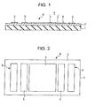
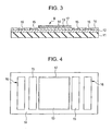
- Figs. 1 and 2 are views showing the structure of the first embodiment of a hydrogen sensor according to the present invention
- a hydrogen sensor A of this embodiment has the following structure. That is, on the approximately entire upper surface of an insulating substrate (insulating base body) 1, a semiconductor layer (semiconductor) 2 is provided, and at a central portion on the upper surface of this semiconductor layer 2, a hydrogen absorber 3 is formed in which particles are dispersed and arranged in the form of islands.
- inside electrodes 5 and 5 and outside electrodes 6 and 6 are provided on the surface of the semiconductor layer 2, the inside electrodes 5 and 5 being located at two sides of the hydrogen absorber 3, the outside electrodes 6 and 6 being located at two sides of the inside electrodes 5 and 5 so as to be further from the center.
- the semiconductor layer 2 and the hydrogen absorber 3 form a hydrogen detection portion 4.
- the insulating substrate (insulating base body) 1 may be a substrate formed of an insulating material, and for example, as the substrate, there may be mentioned a glass and a quartz substrate, such as SiO 2 , a ceramic substrate such as Al 2 O 3 , and a Si substrate used as an insulating substrate which is not doped with ions. Since this insulating substrate 1 may only have insulating properties at an upper surface side thereof, a conductive substrate provided with an insulating layer on the surface thereof may also be used.
- the semiconductor layer 2 has a layer shape formed of a semiconductor, such as ITO (indium tin oxide), GaN, or an n-type Si doped with P.
- a semiconductor material formed by doping an intrinsically insulating material with ions is preferably used.
- this type of semiconductor for example, there may be used an n-type semiconductor formed by doping ions of a V-group element, such as P, As, or Sb, into silicon, or a p-type semiconductor formed by doping ions of a III-group element such as B into silicon.
- an n-type or a p-type SiC, Ge, SiGe, GaAs, or GaN may also be used.
- the hydrogen absorber (hydrogen absorbing material member) 3 preferably has the structure in which particles made of Pd, a Pd alloy, Pt, or a Pt alloy, particles made of another platinum-group element, or particles of an alloy made of the aforementioned element are dispersed and arranged in the form of islands.
- This hydrogen absorber 3 absorbs hydrogen when being placed in an installation environment in which hydrogen is present, and on the contrary, the hydrogen absorber 3 releases absorbed hydrogen when hydrogen is depleted in the installation environment.
- an alloy containing La, Ti, Zr, Mg, a rare earth metal, Ca, V, or the like, which is generally known as an hydrogen absorbing alloy may also be used.
- the hydrogen absorber 3 is composed of a hydrogen-absorbing material, such as the aforementioned metal or the alloy thereof, and when a film is formed on the semiconductor layer 2 using the hydrogen-absorbing material, a pattern thereof must be formed so that electrodes to be formed in a subsequent step are not electrically connected to each other.
- a photolithographic method is preferably used.
- the state is preferably formed in which particles are dispersed in the form of islands which are isolated from each other so that electrical conductivity is not obtained as a whole.
- this hydrogen absorber 3 is simply shown in the form of a film ; however, the hydrogen absorber 3 is preferably formed to have a thickness so as to function as an insulating member. That is, when being magnified, this insulating layer is an aggregate preferably made of particles separately dispersed in the form of islands.
- this insulating layer is an aggregate preferably made of particles separately dispersed in the form of islands.
- an insulating member having a resistance of approximately 1 M ⁇ be used, and that the thickness of the hydrogen absorber 3 be in the range of approximately 0.5 to 5 nm.
- the hydrogen absorber 3 dispersed in the form of islands can be formed using a film-forming method, such as a vacuum deposition method or a sputtering method, in which when particles are deposited on the semiconductor layer 2, the film formation is stopped in a state before the particles are formed into a film.
- a film-forming method such as a vacuum deposition method or a sputtering method, in which when particles are deposited on the semiconductor layer 2, the film formation is stopped in a state before the particles are formed into a film.
- a conductive member is formed.
- the hydrogen absorber 3 can be formed on the semiconductor layer 2 to have a dispersed island structure in which a plurality of particles is dispersed and arranged in the form of islands.
- the hydrogen absorber 3 when being formed to have a thickness in the range described above, can be formed on the semiconductor layer 2 as an insulating member.
- the hydrogen absorber 3 has a longitudinal length slightly smaller than that of the insulating substrate 1 and has a lateral length one severalth of that of the insulating substrate 1. Hence, at the two sides of the hydrogen absorber 3 shown in Figs. 1 and 2 in the lateral direction, the semiconductor layer 2 is exposed.
- the inside electrodes 5 described above are formed on the upper surface of the semiconductor layer 2 so as to be disposed at the two sides of the hydrogen absorber 3 with spaces therefrom.
- the inside electrodes 5 are composed of a good conductive metal material such as Au or Al and are formed by a film-forming method such as a vacuum deposition method, a sputtering method, or a screen-printing method.
- the outside electrodes 6 described above are formed at two end sides of the semiconductor layer 2 so as to sandwich the inside electrodes 5 and 5 from the two sides thereof.
- the hydrogen sensor A In detecting hydrogen using the hydrogen sensor A formed as described above, the hydrogen sensor A is placed in a measurement environment and is used for measurement of the change in electrical resistance of the semiconductor layer 2 itself by measuring the voltage between the inside electrodes 5 and 5 while a predetermined current is applied between the outside electrodes 6 and 6. In this case, what measured by the inside electrodes 5 and 5 corresponds to the change in electrical resistance of the semiconductor layer 2 itself.
- the installation environment of the hydrogen sensor A may be room temperature, and in addition, even in an environment at a temperature slightly higher than that, any problem may not occur.
- conventional hydrogen sensors are generally operated at a high temperature and cannot be reused when reoxidation is not performed at a high temperature such as approximately 200 to 300° C after detection of hydrogen, the hydrogen sensor A having the above structure can be reused when being simply placed in a room-temperature environment after detection of hydrogen.
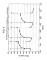
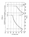
- Figs. 3 and 4 are views showing the structure of the second embodiment of a hydrogen sensor according to the present invention, and a hydrogen sensor B of this embodiment has the following structure. That is, on the approximately entire upper surface of an insulating substrate 11, a semiconductor layer 12 is provided, and inside electrodes 15 and 15 and outside electrodes 16 and 16 are formed at places located at two sides of a central portion on the upper surface of this semiconductor layer 12, the places being equivalent to those of the case of the hydrogen sensor A of the above first embodiment when viewed in plan.
- a thin-film insulating layer 14 is provided so as to cover the peripheral portions of the electrodes 15 and 16 and the other areas, that is, the upper surface of the semiconductor layer 12, and a hydrogen absorber 13 having the structure in which particles are dispersed and arranged in the form of islands is formed so as to be located at the central portion of the upper surface side of the semiconductor layer 12 when viewed in plan. Furthermore, a hydrogen permeable protective film 17 is formed so as to cover the hydrogen absorber 13.
- the hydrogen absorber 13 of this embodiment is formed of a material equivalent to that of the hydrogen absorber 3 of the first embodiment described above, and the size and the shape thereof are formed to be equivalent to those described above.
- the inside electrodes 15 of this embodiment are also formed of a material equivalent to that of the inside electrodes 15 of the first embodiment described above, and the size and the shape thereof are formed to be equivalent to those described above.
- the outside electrodes 16 of this embodiment are also formed of a material equivalent to that of the outside electrodes 16 of the first embodiment described above, and the size and the shape thereof are formed to be equivalent to those described above.
- the hydrogen sensor B of this second embodiment can be used in the same manner as that of the hydrogen sensor A of the first embodiment described above. That is, when the hydrogen sensor B is installed in an environment at room temperature or an environment in which a temperature slightly higher than that is required, and a hydrogen gas is present in this installation environment, hydrogen is absorbed into the hydrogen absorber 13 through the protective film 17, and as a result, the resistance of the semiconductor layer 12 is changed.
- the thin-film insulating layer 14 provided between the semiconductor layer 12 and the hydrogen absorber 13 must have a thickness so as not to interfere with the influence on the semiconductor layer 12 which is generated by hydrogen absorption into the hydrogen absorber 13.
- the thin-film insulating layer 14 at least a part thereof which is used as an underlying layer for the hydrogen absorber 13 preferably has a thickness in the range of approximately 1 to 100 nm.
- the hydrogen sensor A of the first embodiment when being measured by a four-terminal method using the outside electrodes 16 and 16 and the inside electrodes 15 and 15, the change in resistance of the semiconductor layer 12 described above can be accurately measured, and hence hydrogen can be detected.
- the form of the semiconductor as the hydrogen detection portion is not limited to a film.
- the following structure may be formed in which a massive semiconductor or a molded semiconductor having a desired shape formed by compacting semiconductor particles is provided, a pattern of a hydrogen absorber is provided, which does not allow a pair of electrodes to be electrically connected to each other, on a part of the massive semiconductor or the molded semiconductor, and subsequently, inside electrodes and outside electrodes are formed so as to detect the resistance of the semiconductor which is the massive semiconductor or the molded semiconductor.
- An ITO film (indium tin oxide film) having a thickness of 0.01 ⁇ m was formed on a glass substrate 16 mm long and 9 mm wide, and at a central portion of this ITO film, an island-shaped hydrogen absorber film of Pd was formed having a thickness of 12 ⁇ and having a rectangular shape 5 mm long and 7 mm wide.
- the film of this hydrogen absorber was an insulating member on the glass substrate.
- inside electrodes (inside electrodes each having a laminate structure formed of a Ti layer as an underlayer and a Au layer provided thereon) having a size of 1.2 by 7.5 mm made of a Ti/Au layer were first formed on the ITO film and at two sides of the hydrogen absorber with spaces therefrom, and furthermore, outside electrodes made of a Ti/Au layer were formed outside of the inside electrodes at a distance of 1 mm therefrom.
- the hydrogen sensor having this structure was placed in a measuring chamber, and a repetitive hydrogen gas-detection test was performed in which, at a temperature of 30° C (approximately room temperature), the atmospheric environment (100% of air) and a hydrogen gas-containing air environment (1% of a hydrogen gas and 99% of air) were alternately switched over therebetween at every predetermined time interval.
- a temperature of 30° C approximately room temperature
- the atmospheric environment (100% of air) and a hydrogen gas-containing air environment 1% of a hydrogen gas and 99% of air
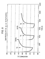
- Fig. 6 is a graph showing the change in resistance in the case in which a hydrogen sensor having the same structure as that of the hydrogen sensor in Example 1 described above was used.
- the environment in the chamber in which this hydrogen sensor was placed was repeatedly and alternately switched over between a nitrogen gas environment containing 1% of a hydrogen gas and a 100% nitrogen gas environment.
- the hydrogen sensor of the present invention and the hydrogen sensor having the conventional structure are compared with each other for further investigation.
- a hydrogen sensor using a conventional oxide semiconductor has been realized by the mechanism in which detection of hydrogen is performed by using a redox reaction, and the detection of hydrogen is performed using a phenomenon in which when a part of the semiconductor is reduced by hydrogen adsorption to form a state in which oxygen is removed, the thickness of the electrical depletion layer of the oxide semiconductor is changed, and as a result, the resistance is changed.
- the oxide semiconductor must be oxidized by heating to a high temperature so that the reduced part thereof is allowed to return to the original state.
- the hydrogen sensor of the present invention even when the environment returns to a 100% nitrogen gas environment, the resistance returns to the original level.
- the change in resistance of the semiconductor layer is not caused by a redox reaction, and the change in resistance is caused, by an electrical conduction mechanism of the semiconductor layer on which the hydrogen absorption into the hydrogen absorber directly acts. Accordingly, it is apparently found that, in the hydrogen sensor of the present invention, the mechanism in which the resistance of the semiconductor is changed is completely different from that of the conventional hydrogen sensor.
- Fig. 7 is a graph showing the change in resistance of a hydrogen sensor having the structure in which a hydrogen absorber of Pd having a thickness of 12 ⁇ was provided on a GaN (Si doped) film having a thickness of 1 ⁇ m used as the semiconductor layer (the thickness and the size of the substrate, electrode, and hydrogen absorber were the same as those in Example 1), the change in resistance being obtained when the environment in the chamber in which this hydrogen sensor was placed was repeatedly and alternately switched over between an atmospheric environment containing 1% of a hydrogen gas and a 100% atmospheric environment at a temperature of 30° C.
- Fig. 8 is a graph showing the change in resistance of a hydrogen sensor having the structure in which a hydrogen absorber of Pd having a thickness of 12 ⁇ was provided on a GaN (Si doped) film having a thickness of 1 ⁇ m used as the semiconductor layer (the thickness and the size of the substrate, electrode, and hydrogen absorber were the same as those in Example 1), the change in resistance being obtained when the environment in the chamber in which this hydrogen sensor was placed was repeatedly and alternately switched over between a nitrogen gas environment containing 1% of a hydrogen gas and a 100% nitrogen gas environment at a temperature of 30° C.
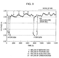
- Fig. 9 is a graph showing the result of the change in resistance of a hydrogen sensor having the structure in which a hydrogen absorber of Pd having a thickness of 12 ⁇ was provided on a GaN (Si doped) film having a thickness of 1 ⁇ m used as the semiconductor layer (the thickness and the size of the substrate, electrode, and hydrogen absorber were the same as those in Example 1), the change in resistance being obtained when the environment in the chamber in which this hydrogen sensor was placed was changed as described below.
- the change in resistance was obtained by switching over twice between an atmospheric environment containing 0.5% of a hydrogen gas and a 100% atmospheric environment at a temperature of 130° C; subsequently, the change in resistance was obtained by supplying gases other than hydrogen, that is, a methane gas (10,000 ppm), a propane gas (10,000 ppm), an isobutane gas (10,000 ppm), and carbon dioxide (8,000 ppm), into the chamber in a time sequential manner, and then allowing the environment to return to the atmosphere after the supply of each of the aforementioned gases; the change in resistance was then obtained by switching over twice between an atmospheric environment containing 0.5% of a hydrogen gas and a 100% atmospheric environment at a temperature of 130° C; and next, a noise component was measured while 100% of air was simply allowed to flow.
- gases other than hydrogen that is, a methane gas (10,000 ppm), a propane gas (10,000 ppm), an isobutane gas (10,000 ppm), and carbon dioxide (8,000 ppm
- the hydrogen sensor of the present invention has an ability of detecting only hydrogen. Comparative Example
- Fig. 10 is a graph showing typical examples of sensitivity of a gas sensor to various gases, the gas sensor having a conventional structure using an SnO 2 oxide semiconductor (for example, see “ Densi Zairyo Ceramic” (Electronic Material Ceramic), first edition, p. 128, published by Ohmsha Ltd. ).
- an n-type oxide semiconductor semiconductor using electrons as charge carriers
- SnO 2 or ZnO semiconductor using electrons as charge carriers
- oxygen is generally adsorbed.
- This adsorbed oxygen pulls electrons out of the semiconductor and are adsorbed as a negative charge, and hence, in the case of an n-type semiconductor, an electrical depletion layer having a thickness of several to several tens nanometers is formed in the surface thereof.
- the adsorbed oxygen ions are in the form of O - or O 2- at a temperature of 200 to 400° C at which the sensor is to be used. When a flammable gas is present in this case, the adsorbed oxygen reacts therewith.
- a reaction theory of a general semiconductor gas sensor has been construed as described above, and this type of semiconductor sensor surely reacts with the various gases as shown in Fig. 10 besides hydrogen.
- the hydrogen sensor according to the present invention reacts with only hydrogen without receiving any influence from other gases, and even when this hydrogen sensor is operated in an oxygen-free environment and is then allowed to return to a 100% nitrogen gas environment which contains no oxygen, the resistance thereof returns to the original level. From the comparison described above, it is apparent that the hydrogen sensor of the present invention is operated in accordance with a mechanism completely different from that for the sensor using an oxide semiconductor described in the conventional example.
Landscapes
- Chemical & Material Sciences (AREA)
- Health & Medical Sciences (AREA)
- Life Sciences & Earth Sciences (AREA)
- Analytical Chemistry (AREA)
- General Health & Medical Sciences (AREA)
- Pathology (AREA)
- Immunology (AREA)
- Physics & Mathematics (AREA)
- Engineering & Computer Science (AREA)
- Biochemistry (AREA)
- General Physics & Mathematics (AREA)
- Combustion & Propulsion (AREA)
- Medicinal Chemistry (AREA)
- Food Science & Technology (AREA)
- Chemical Kinetics & Catalysis (AREA)
- Electrochemistry (AREA)
- Investigating Or Analyzing Materials By The Use Of Fluid Adsorption Or Reactions (AREA)
Claims (10)
- Détecteur d'hydrogène comportant un moyen de détection d'hydrogène composé d'un semi-conducteur (2, 12) et d'un absorbeur d'hydrogène (3, 13) disposés sur au moins une partie d'une surface du semi-conducteur (2, 12), et une paire d'électrodes (5, 15; 6, 16) disposées à la surface du semi-conducteur (2, 12) de façon que l'absorbeur d'hydrogène soit intercalé entre elles et de façon à ne pas être connectées électriquement l'une à l'autre avec l'absorbeur d'hydrogène (3, 13), l'absorbeur d'hydrogène étant placé sur le semi-conducteur afin d'avoir une structure en îlots dispersés dans laquelle une pluralité de particules sont dispersées et organisées sous la forme d'îlots.
- Détecteur d'hydrogène selon la revendication 1, dans lequel le semi-conducteur est un semi-conducteur en forme de couche (2, 12) disposé sur un substrat isolant (1, 11).
- Détecteur d'hydrogène selon la revendication 1 ou 2, dans lequel l'absorbeur d'hydrogène (3) est disposé à la surface du semi-conducteur (2) de manière à être au contact de celle-ci.
- Détecteur d'hydrogène selon la revendication 1 ou 2, dans lequel l'absorbeur d'hydrogène (13) est disposé à la surface du semi-conducteur (12), une couche isolante en film mince (14) étant intercalée entre ceux-ci.
- Détecteur d'hydrogène selon l'une quelconque des revendications 1 à 4, dans lequel une surface découverte du moyen de détection d'hydrogène est couverte par un film (17) perméable à l'hydrogène qui laisse passer l'hydrogène à travers celui-ci.
- Détecteur d'hydrogène selon l'une quelconque des revendications 1 à 5, dans lequel le semi-conducteur est un semi-conducteur non constitué par un oxyde.
- Détecteur d'hydrogène selon la revendication 6, dans lequel le semi-conducteur non constitué par un oxyde est un semi-conducteur non constitué par un oxyde principalement composé d'un semi-conducteur parmi le silicium, le carbure de silicium, le germanium, l'alliage silicium-germanium, le nitrure de gallium et le diamant.
- Détecteur d'hydrogène selon la revendication 5, dans lequel le film perméable à l'hydrogène est composé de nitrure de silicium, d'oxyde de silicium ou de polyimide.
- Procédé pour détecter de l'hydrogène, comportant les étapes de réalisation d'un moyen de détection d'hydrogène composé d'un semi-conducteur (2, 12) et d'un absorbeur d'hydrogène (3, 13) disposés sur au moins une partie d'une surface du semi-conducteur, et une paire d'électrodes (5, 15; 6, 16) disposées à la surface du semi-conducteur de façon que l'absorbeur d'hydrogène (3, 13) soit intercalé entre elles et de façon à ne pas être connectées électriquement l'une à l'autre avec l'absorbeur d'hydrogène, l'absorbeur d'hydrogène (3, 13) étant placé sur le semi-conducteur (2, 12) afin d'avoir une structure en îlots dispersés dans laquelle une pluralité de particules sont dispersées et organisées sous la forme d'îlots ; et de mesure du changement de résistance du semi-conducteur, provoquée par l'absorption d'hydrogène dans l'absorbeur d'hydrogène, le changement étant mesuré entre les deux électrodes, grâce à quoi la présence d'hydrogène est détectée.
- Procédé pour détecter de l'hydrogène selon la revendication 9, dans lequel l'absorbeur d'hydrogène est composé d'un métal parmi le palladium, un alliage de palladium, le platine et un alliage de platine.
Applications Claiming Priority (2)
| Application Number | Priority Date | Filing Date | Title |
|---|---|---|---|
| JP2004133339A JP4056987B2 (ja) | 2004-04-28 | 2004-04-28 | 水素センサ及び水素の検知方法 |
| JP2004133339 | 2004-04-28 |
Publications (2)
| Publication Number | Publication Date |
|---|---|
| EP1591777A1 EP1591777A1 (fr) | 2005-11-02 |
| EP1591777B1 true EP1591777B1 (fr) | 2015-02-25 |
Family
ID=34935824
Family Applications (1)
| Application Number | Title | Priority Date | Filing Date |
|---|---|---|---|
| EP05009229.5A Expired - Lifetime EP1591777B1 (fr) | 2004-04-28 | 2005-04-27 | Capteur d'hydrogène et procédé de détection d'hydrogène |
Country Status (3)
| Country | Link |
|---|---|
| US (1) | US8025843B2 (fr) |
| EP (1) | EP1591777B1 (fr) |
| JP (1) | JP4056987B2 (fr) |
Families Citing this family (22)
| Publication number | Priority date | Publication date | Assignee | Title |
|---|---|---|---|---|
| DE102005057214A1 (de) * | 2005-11-29 | 2007-06-14 | Justus-Liebig-Universität Giessen | Erfindung betreffend Gassensoren |
| US7389675B1 (en) * | 2006-05-12 | 2008-06-24 | The United States Of America As Represented By The National Aeronautics And Space Administration | Miniaturized metal (metal alloy)/ PdOx/SiC hydrogen and hydrocarbon gas sensors |
| JP2008032458A (ja) * | 2006-07-27 | 2008-02-14 | Toyota Central Res & Dev Lab Inc | 水素ガスセンサ |
| WO2008081921A1 (fr) * | 2006-12-28 | 2008-07-10 | Mikuni Corporation | Capteur d'hydrogène et son procédé de fabrication |
| KR100895071B1 (ko) | 2007-07-27 | 2009-04-27 | 재단법인 포항산업과학연구원 | 측온저항체를 이용한 수소 누설 검지센서 및 그 제조방법 |
| US9606078B2 (en) * | 2007-11-11 | 2017-03-28 | University Of North Florida Board Of Trustees | Nanocrystalline indum tin oxide sensors and arrays |
| WO2009126568A1 (fr) * | 2008-04-06 | 2009-10-15 | H2Scan Corporation | Revêtements protecteurs pour capteurs de gaz à semi-conducteurs utilisant des métaux catalytiques |
| WO2011145492A1 (fr) * | 2010-05-17 | 2011-11-24 | 本田技研工業株式会社 | Capteur de gaz de type à combustion catalytique |
| US8839659B2 (en) | 2010-10-08 | 2014-09-23 | Board Of Trustees Of Northern Illinois University | Sensors and devices containing ultra-small nanowire arrays |
| US9618465B2 (en) * | 2013-05-01 | 2017-04-11 | Board Of Trustees Of Northern Illinois University | Hydrogen sensor |
| US10473604B2 (en) * | 2015-06-30 | 2019-11-12 | GM Global Technology Operations LLC | Method of determining deformation location |
| US10054575B2 (en) | 2015-09-25 | 2018-08-21 | General Electric Company | Hydrogen detector and hydrogen detection method |
| JP6840170B2 (ja) * | 2016-12-15 | 2021-03-10 | ヌヴォトンテクノロジージャパン株式会社 | 水素検出装置、燃料電池自動車、水素漏洩監視システム、複合センサモジュール、水素検出方法、およびプログラム |
| WO2019087390A1 (fr) * | 2017-11-06 | 2019-05-09 | キヤノンアネルバ株式会社 | Structure et son procédé de production |
| EP3754329B1 (fr) * | 2019-06-21 | 2023-07-26 | Materion GmbH | Capteur d'hydrogène et son procédé de fabrication, dispositif de mesure et procédé de mesure dune concentration d'hydrogène |
| CN110763413A (zh) * | 2019-10-16 | 2020-02-07 | 顺德职业技术学院 | 产品的捡漏装置及检测方法 |
| JP7486123B2 (ja) * | 2020-07-02 | 2024-05-17 | パナソニックIpマネジメント株式会社 | ガスセンサ装置 |
| CN112345615A (zh) * | 2020-11-03 | 2021-02-09 | 大连理工大学 | 一种氮化镓基高电子迁移率晶体管的氢气传感器 |
| DE102021101360A1 (de) | 2021-01-22 | 2022-07-28 | Vaillant Gmbh | Verfahren und Anordnung zum Erkennen und/oder Beobachten von Flammen in einem Heizgerät |
| CN113155904B (zh) * | 2021-02-02 | 2023-06-20 | 浙江工业大学 | 一种用于空气环境中的高灵敏氢气传感器及其制备方法 |
| CN113406147B (zh) * | 2021-05-08 | 2022-11-29 | 中北大学 | 一种氢气敏感元件及制备方法 |
| US20220404302A1 (en) * | 2021-06-09 | 2022-12-22 | Carrier Corporation | Hydrogen gas sensor assembly |
Family Cites Families (13)
| Publication number | Priority date | Publication date | Assignee | Title |
|---|---|---|---|---|
| GB2043913B (en) | 1979-02-15 | 1983-01-26 | Emi Ltd | Gas detector |
| JPS59120945A (ja) | 1982-12-28 | 1984-07-12 | Shinkosumosu Denki Kk | 水素選択性センサ |
| JPS60211348A (ja) | 1984-04-06 | 1985-10-23 | Matsushita Electric Ind Co Ltd | 水素ガスセンサ− |
| JPH03259736A (ja) | 1990-03-09 | 1991-11-19 | Kurabe Ind Co Ltd | 水素ガス検知素子 |
| US5229610A (en) * | 1991-02-06 | 1993-07-20 | Colorado School Of Mines | Method and apparatus for detecting hydrogen-containing compounds |
| JP3259736B2 (ja) | 1992-05-18 | 2002-02-25 | 株式会社安川電機 | 数値制御ネジ切り装置 |
| JPH06148112A (ja) | 1992-10-30 | 1994-05-27 | Kurabe Ind Co Ltd | 水素ガス検知素子 |
| US5520753A (en) | 1994-12-30 | 1996-05-28 | The United States Of America As Represented By The Administrator Of The National Aeronautics And Space Administration | PDTI metal alloy as a hydrogen or hydrocarbon sensitive metal |
| DE10105581C1 (de) | 2001-02-07 | 2002-11-28 | Siemens Ag | Resistiver Galliumoxid-Wasserstoffsensor |
| JP2002328109A (ja) | 2001-05-02 | 2002-11-15 | Ngk Spark Plug Co Ltd | 水素ガス検出素子及びその製造方法 |
| JP2002328108A (ja) | 2001-05-02 | 2002-11-15 | Ngk Spark Plug Co Ltd | 水素ガス検出素子及びその製造方法 |
| JP3698679B2 (ja) * | 2002-03-27 | 2005-09-21 | 株式会社日立製作所 | ガス流量計及びその製造方法 |
| JP5401817B2 (ja) * | 2008-03-25 | 2014-01-29 | 富士通セミコンダクター株式会社 | 半導体装置の製造方法及び半導体装置 |
-
2004
- 2004-04-28 JP JP2004133339A patent/JP4056987B2/ja not_active Expired - Fee Related
-
2005
- 2005-04-22 US US11/112,231 patent/US8025843B2/en not_active Expired - Fee Related
- 2005-04-27 EP EP05009229.5A patent/EP1591777B1/fr not_active Expired - Lifetime
Also Published As
| Publication number | Publication date |
|---|---|
| JP4056987B2 (ja) | 2008-03-05 |
| EP1591777A1 (fr) | 2005-11-02 |
| JP2005315700A (ja) | 2005-11-10 |
| US8025843B2 (en) | 2011-09-27 |
| US20050258051A1 (en) | 2005-11-24 |
Similar Documents
| Publication | Publication Date | Title |
|---|---|---|
| EP1591777B1 (fr) | Capteur d'hydrogène et procédé de détection d'hydrogène | |
| EP2044424B1 (fr) | Procédé pour fabriquer un détecteur de gaz présentant des nanostructures d'oxyde de zinc | |
| Traversa | Design of ceramic materials for chemical sensors with novel properties | |
| US4892834A (en) | Chemical sensor | |
| Gardner et al. | Integrated tin oxide odour sensors | |
| EP3786627B1 (fr) | Élément de détection de gaz à semi-conducteur de type mems | |
| Gas' Kov et al. | Nature of gas sensitivity in nanocrystalline metal oxides | |
| JP3128114B2 (ja) | 窒素酸化物検出装置 | |
| JP2011203256A (ja) | センシング用アモルファス薄膜 | |
| US20110138882A1 (en) | Semiconductor gas sensor having low power consumption | |
| EP1693667B1 (fr) | Capteur de gaz | |
| KR20110066849A (ko) | 저전력소모형 반도체 가스 센서 | |
| JP3812215B2 (ja) | 薄膜ガスセンサ | |
| Liu et al. | A low power bridge-type gas sensor with enhanced sensitivity to ethanol by sandwiched ZnO/Au/ZnO film sputtered in O₂ atmosphere | |
| WO1998032007A1 (fr) | Procede de detection d'oxydes d'azote et element de capteur permettant de detecter des oxydes azotes | |
| Sulz et al. | Ni, In and Sb implanted Pt and V catalysed thin-film SnO2 gas sensors | |
| CN118090867B (zh) | 一种fet氢气传感器及其制备方法 | |
| JP4355300B2 (ja) | 水素透過膜、水素センサおよび水素の検知方法 | |
| JP2005030907A (ja) | ガスセンサ | |
| KR20090011631A (ko) | 가스 센서 및 그 제조 방법 | |
| JP3075070B2 (ja) | 一酸化炭素ガスセンサ | |
| JP4340639B2 (ja) | 水素センサ及び水素の検知方法 | |
| EP2466298A1 (fr) | Procédé de fabrication d'une structure conductrice électrique, procédé de fabrication d'un capteur de gaz, capteur de gaz obtenu avec le procédé et utilisation du capteur de gaz permettant de détecter un gaz | |
| CN116990374B (en) | MOSFET gas sensor and preparation method thereof | |
| Nakamura et al. | Electric Control of the Chemical Reaction in Ceramic–Ceramic Contact Interface—Modeling of the Reaction Scheme |
Legal Events
| Date | Code | Title | Description |
|---|---|---|---|
| PUAI | Public reference made under article 153(3) epc to a published international application that has entered the european phase |
Free format text: ORIGINAL CODE: 0009012 |
|
| AK | Designated contracting states |
Kind code of ref document: A1 Designated state(s): AT BE BG CH CY CZ DE DK EE ES FI FR GB GR HU IE IS IT LI LT LU MC NL PL PT RO SE SI SK TR |
|
| AX | Request for extension of the european patent |
Extension state: AL BA HR LV MK YU |
|
| 17P | Request for examination filed |
Effective date: 20051124 |
|
| AKX | Designation fees paid |
Designated state(s): DE FR GB SE |
|
| 17Q | First examination report despatched |
Effective date: 20090213 |
|
| GRAP | Despatch of communication of intention to grant a patent |
Free format text: ORIGINAL CODE: EPIDOSNIGR1 |
|
| INTG | Intention to grant announced |
Effective date: 20140911 |
|
| GRAS | Grant fee paid |
Free format text: ORIGINAL CODE: EPIDOSNIGR3 |
|
| GRAA | (expected) grant |
Free format text: ORIGINAL CODE: 0009210 |
|
| AK | Designated contracting states |
Kind code of ref document: B1 Designated state(s): DE FR GB SE |
|
| REG | Reference to a national code |
Ref country code: GB Ref legal event code: FG4D |
|
| REG | Reference to a national code |
Ref country code: DE Ref legal event code: R096 Ref document number: 602005045869 Country of ref document: DE Effective date: 20150409 |
|
| PG25 | Lapsed in a contracting state [announced via postgrant information from national office to epo] |
Ref country code: SE Free format text: LAPSE BECAUSE OF FAILURE TO SUBMIT A TRANSLATION OF THE DESCRIPTION OR TO PAY THE FEE WITHIN THE PRESCRIBED TIME-LIMIT Effective date: 20150225 |
|
| PGFP | Annual fee paid to national office [announced via postgrant information from national office to epo] |
Ref country code: DE Payment date: 20150421 Year of fee payment: 11 |
|
| REG | Reference to a national code |
Ref country code: DE Ref legal event code: R097 Ref document number: 602005045869 Country of ref document: DE |
|
| PLBE | No opposition filed within time limit |
Free format text: ORIGINAL CODE: 0009261 |
|
| STAA | Information on the status of an ep patent application or granted ep patent |
Free format text: STATUS: NO OPPOSITION FILED WITHIN TIME LIMIT |
|
| GBPC | Gb: european patent ceased through non-payment of renewal fee |
Effective date: 20150525 |
|
| REG | Reference to a national code |
Ref country code: FR Ref legal event code: ST Effective date: 20151231 |
|
| 26N | No opposition filed |
Effective date: 20151126 |
|
| PG25 | Lapsed in a contracting state [announced via postgrant information from national office to epo] |
Ref country code: FR Free format text: LAPSE BECAUSE OF NON-PAYMENT OF DUE FEES Effective date: 20150430 |
|
| PG25 | Lapsed in a contracting state [announced via postgrant information from national office to epo] |
Ref country code: GB Free format text: LAPSE BECAUSE OF NON-PAYMENT OF DUE FEES Effective date: 20150525 |
|
| REG | Reference to a national code |
Ref country code: DE Ref legal event code: R119 Ref document number: 602005045869 Country of ref document: DE |
|
| PG25 | Lapsed in a contracting state [announced via postgrant information from national office to epo] |
Ref country code: DE Free format text: LAPSE BECAUSE OF NON-PAYMENT OF DUE FEES Effective date: 20161101 |