EP1592076A2 - Dispositif optoélectronique à plusieurs couches de diffusion de courant - Google Patents
Dispositif optoélectronique à plusieurs couches de diffusion de courant Download PDFInfo
- Publication number
- EP1592076A2 EP1592076A2 EP05008670A EP05008670A EP1592076A2 EP 1592076 A2 EP1592076 A2 EP 1592076A2 EP 05008670 A EP05008670 A EP 05008670A EP 05008670 A EP05008670 A EP 05008670A EP 1592076 A2 EP1592076 A2 EP 1592076A2
- Authority
- EP
- European Patent Office
- Prior art keywords
- current spreading
- layer
- spreading layer
- optoelectronic component
- component according
- Prior art date
- Legal status (The legal status is an assumption and is not a legal conclusion. Google has not performed a legal analysis and makes no representation as to the accuracy of the status listed.)
- Granted
Links
Images

Classifications
-
- H—ELECTRICITY
- H10—SEMICONDUCTOR DEVICES; ELECTRIC SOLID-STATE DEVICES NOT OTHERWISE PROVIDED FOR
- H10H—INORGANIC LIGHT-EMITTING SEMICONDUCTOR DEVICES HAVING POTENTIAL BARRIERS
- H10H20/00—Individual inorganic light-emitting semiconductor devices having potential barriers, e.g. light-emitting diodes [LED]
- H10H20/80—Constructional details
- H10H20/83—Electrodes
- H10H20/832—Electrodes characterised by their material
-
- H—ELECTRICITY
- H10—SEMICONDUCTOR DEVICES; ELECTRIC SOLID-STATE DEVICES NOT OTHERWISE PROVIDED FOR
- H10H—INORGANIC LIGHT-EMITTING SEMICONDUCTOR DEVICES HAVING POTENTIAL BARRIERS
- H10H20/00—Individual inorganic light-emitting semiconductor devices having potential barriers, e.g. light-emitting diodes [LED]
- H10H20/80—Constructional details
- H10H20/81—Bodies
- H10H20/822—Materials of the light-emitting regions
- H10H20/824—Materials of the light-emitting regions comprising only Group III-V materials, e.g. GaP
- H10H20/825—Materials of the light-emitting regions comprising only Group III-V materials, e.g. GaP containing nitrogen, e.g. GaN
-
- H—ELECTRICITY
- H10—SEMICONDUCTOR DEVICES; ELECTRIC SOLID-STATE DEVICES NOT OTHERWISE PROVIDED FOR
- H10H—INORGANIC LIGHT-EMITTING SEMICONDUCTOR DEVICES HAVING POTENTIAL BARRIERS
- H10H20/00—Individual inorganic light-emitting semiconductor devices having potential barriers, e.g. light-emitting diodes [LED]
- H10H20/80—Constructional details
- H10H20/83—Electrodes
- H10H20/831—Electrodes characterised by their shape
-
- Y—GENERAL TAGGING OF NEW TECHNOLOGICAL DEVELOPMENTS; GENERAL TAGGING OF CROSS-SECTIONAL TECHNOLOGIES SPANNING OVER SEVERAL SECTIONS OF THE IPC; TECHNICAL SUBJECTS COVERED BY FORMER USPC CROSS-REFERENCE ART COLLECTIONS [XRACs] AND DIGESTS
- Y10—TECHNICAL SUBJECTS COVERED BY FORMER USPC
- Y10S—TECHNICAL SUBJECTS COVERED BY FORMER USPC CROSS-REFERENCE ART COLLECTIONS [XRACs] AND DIGESTS
- Y10S438/00—Semiconductor device manufacturing: process
- Y10S438/942—Masking
- Y10S438/947—Subphotolithographic processing
Definitions
- the invention relates to an optoelectronic device according to the preamble of claim 1 and a method to its production.
- the contacting of radiation-emitting optoelectronic Components is usually done by applying a metallic terminal on the semiconductor chip, the contains the active zone. Often that is for contacting provided surface of the semiconductor chip simultaneously to Radiation extraction provided, so that for the emitted radiation not transparent terminal contact only can be applied to a portion of the surface.
- Such current spreading layers should be ohmic Ensure contact with the semiconductor as well as transparent, be temperature and aging stable. Further should be the application of such a current spreading layer in easy way into the manufacturing process of can be integrated optoelectronic component. These multiple requirements limit the choice of materials for Such current spreading layers significantly.
- a homogeneous current density over the chip area can in particular by a large-scale current spreading layer, which reaches as far as the side edges of the semiconductor chip, be achieved.
- electrostatic discharges ESD - Electro Static Discharge
- This danger exists especially in the case of radiation-emitting semiconductor chips the base of III-V nitride compound semiconductors, since these comparatively high internal electric fields occur.
- the invention is based on the object Specify optoelectronic component, which is characterized by a as homogeneous as possible lateral distribution of the current density and characterized at the same time by a high ESD resistance.
- An optoelectronic component with a semiconductor chip the one semiconductor layer sequence with a radiation-emitting active zone, wherein the Semiconductor layer sequence has side edges, and a Connection contact for current injection into the active zone, contains according to the invention between the Semiconductor layer sequence and the terminal contact a first, to a semiconductor layer of the semiconductor layer sequence adjacent current spreading layer, and a second Current spreading layer, wherein the first Current spreading layer a greater sheet resistance than having the second current spreading layer and a ohmic contact with the adjacent semiconductor layer forms and the second current spreading layer on a Part of the first current spreading layer applied is, which is spaced from the side edges, preferably such that the partial area does not touch the side flanks borders.
- the sheet resistance is a quantity related to a square unit area and is therefore often referred to as a square resistor or indicated in the added unit ⁇ / square.
- the SI unit ⁇ without characteristic additives is continuously used for the sheet resistance.
- the risk of voltage flashovers on the side edges of the semiconductor chip is advantageously reduced and thus increases the ESD resistance.
- the first current spreading layer advantageously has a spacing of less than 3 ⁇ m in the lateral direction to the side flanks of the semiconductor layer sequence or even extends as far as the side flanks.
- the first current spreading layer can also be applied over the whole area to the semiconductor layer sequence.
- the sheet resistance of the first current spreading layer is preferably more than 1000 ⁇ to a high ESD strength to achieve. Such a high sheet resistance can be achieved, for example, that a very thin first current impurity layer is used. Prefers For example, the first current spreading layer is less than 2 nm thick.
- the sheet resistance of the second Current spreading layer should be as low as possible.
- the second current spreading layer may be from the semiconductor chip seen from one or more others Followed by current spreading layers.
- the several Stromaufweitungs slaughteren are preferably stepped Applied to each other, so that each subsequent Current spreading layer only a portion of her previous Stromaufweitungs slaughter covered.
- the invention is not limited to a particular embodiment the semiconductor layer sequence limited, in particular the optoelectronic device any for LEDs or Have laser diodes known semiconductor layer sequence.
- the invention is particularly advantageous for optoelectronic Components in which the semiconductor layer sequence is a III-V nitride compound semiconductor material contains. Bei on this Semiconductor materials based optoelectronic Components is at risk of ESD voltage flashover the side edges particularly high, as in these electrical Fields with an electric field strength of a few MV / cm may occur.
- the adjacent to the first current spreading layer Semiconductor layer may in particular a p-doped Semiconductor layer of a III-V nitride compound semiconductor be.
- a p-doped III-V nitride compound semiconductor the transverse conductivity is so low that without the Inserting current spreading layers of the current flow in the essential to an area below the Terminal would limit, and therefore a large Part of the emitted radiation due to absorption in the Connection contact would be lost.
- the semiconductor layer sequence may include the III-V nitride compound semiconductor material Al x Ga y In 1-xy N, where 0 ⁇ x ⁇ 1, 0 ⁇ y ⁇ 1, and x + y ⁇ 1.
- the first current spreading layer preferably contains one of Materials platinum, palladium or nickel. These are advantageous for forming an ohmic contact on a III-V nitride compound semiconductor material suitable. Thereby, that the ohmic contact with the first Stromaufweitungs slaughter is made, consists in the second Stromaufffles harsh greater freedom of Material selection. This can in particular Au, Pd, ZnO or ITO contain.
- the invention is particularly advantageous for optoelectronic components which have a semiconductor layer sequence with a width of 200 ⁇ m or less, since these components require the most homogeneous possible distribution of the current density into the vicinity of the side edges in order to effectively effect the comparatively small area of the semiconductor chip exploit.
- an inventive optoelectronic component becomes a substrate provided a semiconductor layer sequence on the Substrate applied, at least two Current spreading layers on the semiconductor layer sequence applied and then a mask layer on the Current spreading layers applied and patterned.
- a Protective layer of a silicon oxide, a silicon nitride or a Siliziumoxidnitrid on the last applied Stromaufweitungstik be applied to the Semiconductor layer sequence when removing the mask layer to protect.
- This protective layer can be in a later following Etching process are removed.
- the structuring of the first current spreading layer takes place by an etching process, preferably by a Dry etching process in which the side flanks of the Mask layer less undercut than the following described structuring the second Current spreading layer.
- the side flanks are preferred the mask layer when structuring the first Current spreading layer not undercut at all.
- this process step ie with the same mask layer, also the Semiconductor string sequence is structured. Of the Production costs are reduced.
- the second current spreading layer is replaced by a Etched process structured in which the side edges of the Mask layer are undercut. This is preferably done with a wet-chemical etching process. This is an etchant used by the first current spreading layer and the semiconductor layer sequence is not etched. The optionally applied protective layer is subsequently in a further etching process of the Current spreading layers removed.
- the specified process steps do not have to necessarily in the order described above be performed.
- the second Current spreading layer by means of an etching process, in which the mask layer is undercut, and then the first Current spreading layer with an etching process in which the Mask layer is less or not undercut, be structured.
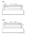
- Optoelectronic component includes a substrate 2 on which a semiconductor layer sequence 6 is applied.
- the Semiconductor layer sequence 6 contains at least one n-doped Semiconductor layer 3 and at least one p-doped Semiconductor layer 5, between which an active zone. 4 is trained.
- the semiconductor layer sequence 6 has a Mesastructure, which in the lateral direction through the Side edges 10 is limited. The side edges 10 must not, as shown in Figure 1, perpendicular to the Semiconductor layer sequence 6 run, but can alternatively also obliquely to the semiconductor layer sequence 6 be curved or curved.
- first Current spreading layer 7 On the p-type semiconductor layer 5 is a first Current spreading layer 7 applied. On a subarea the first current spreading layer 7, which in lateral Direction a distance d of more than 100 nm to the Side flanks 10 of the mesa structure is a second Current spreading layer 8 applied. The sheet resistance the first current spreading layer 7 is at least one Factor 10 greater than the sheet resistance of the second Stromaufweitungstik 8. For electrical contacting of the Optoelectronic device are a first Terminal contact 1 on the of the semiconductor layer sequence. 6 opposite side of the substrate 2 and a second Terminal contact 9 on a portion of the second Current spreading layer 8 is provided.
- Such a stepped arrangement of at least two Stromaufweitungs slaughteren 7, 8 between the Semiconductor layer sequence 6 and the terminal contact 9 acts beneficial in several ways to the operation of the radiation-emitting optoelectronic component.
- a comparatively homogeneous Current density distribution close to the side edges of the Mesa structure reaches 10. This can be a high brightness of the component and a relatively low Forward voltage can be achieved.
- the Current density within the second current spreading layer 8 at an operating current of, for example, about 20 mA by about 5% to 30% from center to edge.
- This Current density gradient increases within the first Current spreading layer 7.
- high currents of, for example, about 1 A. occurs then decrease in current density to the sidewalls 10 of the mesa structure sufficiently large that no Arcing on the side edges 10 done.
- the illustrated in Figure 2 embodiment of the invention differs from that shown in Figure 1 by that between the second current spreading layer 8 and the Terminal 9 a third current spreading layer 11th is included, which refers to a subsection of the second Current spreading layer 8 is applied.
- the third current spreading layer 11 in the direction to the second terminal contact 9 also still be downstream of further Stromaufweitungs slaughteren, wherein it is advantageous if each subordinate Stromaufweitungs slaughter each a portion of hers covered preceding Stromaufweitungstik and a has lower sheet resistance than yours preceding current spreading layer.
- This step-shaped Arrangement of several current spreading layers 7, 8, 11 causes a particularly homogeneous lateral distribution of the current density in the optoelectronic component.
- first Current spreading layer 7 is preferably less than 2 nm thick metal layer, for example, Pt, Pd or Ni contains.
- Preferred materials for the second Current spreading layer are Au, Pd, ZnO and ITO.
- the Stromaufweitungs slaughteren 7, 8, 11 can only be applied selectively or for example due to a very small thickness, a network or island-like structure exhibit. In this case, within the Stromaufweitungs slaughteren in the lateral direction not necessarily formed closed current paths.
- a semitransparent execution of Stromaufweitungs slaughteren 7, 8, 11 is useful if through the areas covered by the current spreading layers Radiation decoupled from the optoelectronic component shall be.
- one or more of the Stromaufweitungs slaughteren 7, 8, 11 also as a reflective Layers are performed, for example, absorption emitted radiation in the terminal contact 9 to prevent.
- This design is also advantageous when it comes to the optoelectronic component is an LED at the radiation in the lateral direction or through the Substrate 2 is coupled out.
- one or more of the Stromaufweitungs slaughter 7, 8, 11 in the lateral direction a variable layer thickness and / or composition exhibit. This is another beneficial option the current density distribution in the lateral direction targeted adjust.
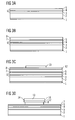
- Figures 3a to 3g are various intermediate stages a method according to the invention for producing a Optoelectronic device shown.
- FIG. 3 a shows a semiconductor substrate 2 onto which a Semiconductor layer sequence 6 is applied, the at least an n-doped semiconductor layer 3 and at least one p-doped Semiconductor layer 5, between which a radiation-emitting active zone 4 is formed.
- the Surface of the semiconductor layer sequence 6 can before the subsequent application of the current spreading layers be roughened.
- the of the semiconductor layer sequence 6th remote from the rear side of the substrate 2 is a first Connection contact 1 provided.
- first current spreading layer 7 for example, about 0.3 nm thick platinum layer
- second Current spreading layer 8 for example, about 6 nm thick gold layer
- a mask layer 13 for example, a photoresist layer applied.
- the protective layer 12 is about 150, for example nm thick.
- it contains a silica, a Silicon nitride or in silicon nitride.
- the second current spreading layer 8 and the protective layer 12 by a wet chemical etching process in which the Side flanks 14 of the mask layer 13 are undercut, been structured.
- An etchant is used through which the first current spreading layer 7 is not or only is slightly attacked.
- the material of the second Stromaufweitungs slaughter 8 must therefore wet-chemically selective to first current spreading layer be etchable.
- the first current spreading layer 7 structured.
- the side edges 14 of Mask layer 13 very little or not at all undercut, so that the structure of the mask layer 13 on the first current spreading layer 7 is transmitted. It forms a step between the first current spreading layer. 7 and the second current spreading layer 8.
- the mesa structure of Semiconductor layer sequence 6 is generated so that the in FIG 3e structure shown.
- the stage between the first current spreading layer 7 and the second Stromaufweitungstik 8 should be at least as wide that the second current spreading layer is an 8 distance from at least 100 nm to the side edges. Perhaps it may be necessary to the second Current spreading layer 8 after forming the mesa structure nachzeticianen wet-chemically.
- the invention is not by the description based on the Embodiments limited. Rather, the includes Invention every new feature as well as every combination of Characteristics, which in particular any combination of features in the patent claims, even if this feature or that combination itself is not explicit in the Claims or embodiments is given.
Landscapes
- Led Devices (AREA)
- Semiconductor Lasers (AREA)
Applications Claiming Priority (4)
| Application Number | Priority Date | Filing Date | Title |
|---|---|---|---|
| DE102004021419 | 2004-04-30 | ||
| DE102004021419 | 2004-04-30 | ||
| DE102004025610A DE102004025610A1 (de) | 2004-04-30 | 2004-05-25 | Optoelektronisches Bauelement mit mehreren Stromaufweitungsschichten und Verfahren zu dessen Herstellung |
| DE102004025610 | 2004-05-25 |
Publications (3)
| Publication Number | Publication Date |
|---|---|
| EP1592076A2 true EP1592076A2 (fr) | 2005-11-02 |
| EP1592076A3 EP1592076A3 (fr) | 2007-10-17 |
| EP1592076B1 EP1592076B1 (fr) | 2009-06-10 |
Family
ID=34935474
Family Applications (1)
| Application Number | Title | Priority Date | Filing Date |
|---|---|---|---|
| EP05008670A Expired - Lifetime EP1592076B1 (fr) | 2004-04-30 | 2005-04-20 | Dispositif optoélectronique à plusieurs couches de diffusion de courant |
Country Status (4)
| Country | Link |
|---|---|
| US (2) | US7227191B2 (fr) |
| EP (1) | EP1592076B1 (fr) |
| JP (1) | JP4970739B2 (fr) |
| DE (2) | DE102004025610A1 (fr) |
Families Citing this family (18)
| Publication number | Priority date | Publication date | Assignee | Title |
|---|---|---|---|---|
| WO2007081719A2 (fr) | 2006-01-05 | 2007-07-19 | Illumitex, Inc. | Dispositif optique séparé pour diriger de la lumière depuis une del |
| US8087960B2 (en) | 2006-10-02 | 2012-01-03 | Illumitex, Inc. | LED system and method |
| WO2008073400A1 (fr) | 2006-12-11 | 2008-06-19 | The Regents Of The University Of California | Diodes électroluminescentes transparentes |
| TWI366291B (en) * | 2007-03-30 | 2012-06-11 | Epistar Corp | Semiconductor light-emitting device having stacked transparent electrodes |
| JP4805887B2 (ja) * | 2007-09-05 | 2011-11-02 | 株式会社東芝 | 半導体レーザ装置 |
| DE102007043681B4 (de) | 2007-09-13 | 2022-01-20 | OSRAM Opto Semiconductors Gesellschaft mit beschränkter Haftung | Optoelektronisches Bauelement |
| JP2011512037A (ja) | 2008-02-08 | 2011-04-14 | イルミテックス, インコーポレイテッド | エミッタ層成形のためのシステムおよび方法 |
| DE102008035110A1 (de) | 2008-07-28 | 2010-02-11 | Osram Opto Semiconductors Gmbh | Optoelektronischer Halbleiterchip |
| TW201034256A (en) | 2008-12-11 | 2010-09-16 | Illumitex Inc | Systems and methods for packaging light-emitting diode devices |
| US8449128B2 (en) | 2009-08-20 | 2013-05-28 | Illumitex, Inc. | System and method for a lens and phosphor layer |
| US8585253B2 (en) | 2009-08-20 | 2013-11-19 | Illumitex, Inc. | System and method for color mixing lens array |
| DE102012112771A1 (de) * | 2012-12-20 | 2014-06-26 | Osram Opto Semiconductors Gmbh | Verfahren zur Herstellung eines optoelektronischen Halbleiterchips und optoelektronischer Halbleiterchip |
| DE102013104272A1 (de) * | 2013-04-26 | 2014-10-30 | Osram Opto Semiconductors Gmbh | Optoelektronisches Bauelement und Verfahren zu seiner Herstellung |
| DE102014111482B4 (de) * | 2014-08-12 | 2025-12-11 | OSRAM Opto Semiconductors Gesellschaft mit beschränkter Haftung | Verfahren zur Herstellung eines optoelektronischen Halbleiterchips |
| KR102506957B1 (ko) * | 2016-02-02 | 2023-03-08 | 쑤저우 레킨 세미컨덕터 컴퍼니 리미티드 | 발광소자 |
| US12300966B2 (en) * | 2019-09-17 | 2025-05-13 | Mitsubishi Electric Corporation | Semiconductor laser device |
| US11592166B2 (en) | 2020-05-12 | 2023-02-28 | Feit Electric Company, Inc. | Light emitting device having improved illumination and manufacturing flexibility |
| US11876042B2 (en) | 2020-08-03 | 2024-01-16 | Feit Electric Company, Inc. | Omnidirectional flexible light emitting device |
Family Cites Families (13)
| Publication number | Priority date | Publication date | Assignee | Title |
|---|---|---|---|---|
| EP0224614B1 (fr) * | 1985-12-06 | 1990-03-14 | International Business Machines Corporation | Procédé de fabrication d'un transistor à effet de champ entièrement auto-aligné |
| US5233204A (en) | 1992-01-10 | 1993-08-03 | Hewlett-Packard Company | Light-emitting diode with a thick transparent layer |
| US6936859B1 (en) | 1998-05-13 | 2005-08-30 | Toyoda Gosei Co., Ltd. | Light-emitting semiconductor device using group III nitride compound |
| DE19921987B4 (de) * | 1998-05-13 | 2007-05-16 | Toyoda Gosei Kk | Licht-Abstrahlende Halbleitervorrichtung mit Gruppe-III-Element-Nitrid-Verbindungen |
| JP4815732B2 (ja) * | 1998-12-08 | 2011-11-16 | 日亜化学工業株式会社 | 窒化物半導体素子 |
| JP3705016B2 (ja) * | 1999-06-28 | 2005-10-12 | 豊田合成株式会社 | 透光性電極用膜及びiii族窒化物系化合物半導体素子 |
| TW439304B (en) * | 2000-01-05 | 2001-06-07 | Ind Tech Res Inst | GaN series III-V compound semiconductor devices |
| JP4810746B2 (ja) * | 2000-03-31 | 2011-11-09 | 豊田合成株式会社 | Iii族窒化物系化合物半導体素子 |
| JP5283293B2 (ja) * | 2001-02-21 | 2013-09-04 | ソニー株式会社 | 半導体発光素子 |
| JP2003086843A (ja) * | 2001-09-14 | 2003-03-20 | Sharp Corp | 半導体発光素子及び半導体発光装置 |
| JP4089194B2 (ja) * | 2001-09-28 | 2008-05-28 | 日亜化学工業株式会社 | 窒化物半導体発光ダイオード |
| DE10261676A1 (de) * | 2002-12-31 | 2004-07-22 | Osram Opto Semiconductors Gmbh | Leuchtdioden-Chip mit strahlungsdurchlässiger elektrischer Stromaufweitungsschicht |
| KR100593886B1 (ko) * | 2003-06-24 | 2006-07-03 | 삼성전기주식회사 | 질화갈륨계 반도체 발광소자의 제조방법 |
-
2004
- 2004-05-25 DE DE102004025610A patent/DE102004025610A1/de not_active Withdrawn
-
2005
- 2005-04-20 DE DE502005007446T patent/DE502005007446D1/de not_active Expired - Lifetime
- 2005-04-20 EP EP05008670A patent/EP1592076B1/fr not_active Expired - Lifetime
- 2005-04-28 JP JP2005133568A patent/JP4970739B2/ja not_active Expired - Lifetime
- 2005-05-02 US US11/120,514 patent/US7227191B2/en not_active Expired - Lifetime
-
2007
- 2007-06-04 US US11/810,326 patent/US7742677B2/en not_active Expired - Lifetime
Also Published As
| Publication number | Publication date |
|---|---|
| EP1592076A3 (fr) | 2007-10-17 |
| EP1592076B1 (fr) | 2009-06-10 |
| JP4970739B2 (ja) | 2012-07-11 |
| US7742677B2 (en) | 2010-06-22 |
| DE502005007446D1 (de) | 2009-07-23 |
| US20070238210A1 (en) | 2007-10-11 |
| US20050253163A1 (en) | 2005-11-17 |
| JP2005322913A (ja) | 2005-11-17 |
| DE102004025610A1 (de) | 2005-11-17 |
| US7227191B2 (en) | 2007-06-05 |
Similar Documents
| Publication | Publication Date | Title |
|---|---|---|
| EP1592076B1 (fr) | Dispositif optoélectronique à plusieurs couches de diffusion de courant | |
| EP2499668B9 (fr) | Composant semi-conducteur à couche mince pourvu d'une structure à diodes de protection, et procédé de production d'un composant semi-conducteur à couche mince | |
| DE102009060747B4 (de) | Halbleiterchip | |
| EP2596532B1 (fr) | Composant optoélectronique | |
| DE202009018090U1 (de) | Halbleiter-Lichtemittervorrichtung | |
| DE19817368A1 (de) | Leuchtdiode | |
| WO2012130900A1 (fr) | Puce semi-conductrice optoélectronique | |
| DE102005061797A1 (de) | Lumineszenzdiodenchip mit Stromaufweitungsschicht und Verfahren zu dessen Herstellung | |
| DE102007046519A1 (de) | Dünnfilm-LED mit einer Spiegelschicht und Verfahren zu deren Herstellung | |
| DE19945134C2 (de) | Lichtemittierendes Halbleiterbauelement hoher ESD-Festigkeit und Verfahren zu seiner Herstellung | |
| EP1658643B1 (fr) | Dispositif a semi-conducteur emetteur de rayonnement | |
| DE10346605B4 (de) | Strahlungemittierendes Halbleiterbauelement | |
| DE102017117164A1 (de) | Optoelektronischer Halbleiterchip, Hochvolthalbleiterchip und Verfahren zur Herstellung eines optoelektronischen Halbleiterchips | |
| WO2020234112A1 (fr) | Puce semi-conductrice optoélectronique | |
| DE102004026231B4 (de) | Verfahren zur Herstellung eines Bereichs mit reduzierter elektrischer Leitfähigkeit innerhalb einer Halbleiterschicht und optoelektronisches Halbleiterbauelement | |
| DE10300949B4 (de) | Halbleitervorrichtung mit Herstellungsverfahren dafür | |
| EP2304816B1 (fr) | Dispositif électroluminescent et procédé de production d'un dispositif électroluminescent | |
| DE102017123755A1 (de) | Verfahren zur Herstellung eines Laserdiodenbarrens und Laserdiodenbarren | |
| DE10147791A1 (de) | Verfahren zur Herstellung eines Halbleiterbauelements auf der Basis eines Nitrid-Verbindungshalbleiters | |
| DE10329079B4 (de) | Strahlungsemittierendes Halbleiterbauelement | |
| EP1649497B1 (fr) | Procede de fabrication d'une pluralite de puces a semi-conducteur optoelectroniques et puce a semi-conducteur optoelectronique ainsi obtenue | |
| DE10155442A1 (de) | Ohmsche Kontaktstruktur und Verfahren zu deren Herstellung | |
| WO2013041279A1 (fr) | Puce de semi-conducteur émettant un rayonnement | |
| DE10346606A1 (de) | Strahlungsemittierendes Halbleiterbauelement | |
| DE10335081A1 (de) | Verfahren zur Herstellung einer Vielzahl von optoelektronischen Halbleiterchips und optoeleketronischer Halbleiterchip |
Legal Events
| Date | Code | Title | Description |
|---|---|---|---|
| PUAI | Public reference made under article 153(3) epc to a published international application that has entered the european phase |
Free format text: ORIGINAL CODE: 0009012 |
|
| AK | Designated contracting states |
Kind code of ref document: A2 Designated state(s): AT BE BG CH CY CZ DE DK EE ES FI FR GB GR HU IE IS IT LI LT LU MC NL PL PT RO SE SI SK TR |
|
| AX | Request for extension of the european patent |
Extension state: AL BA HR LV MK YU |
|
| PUAL | Search report despatched |
Free format text: ORIGINAL CODE: 0009013 |
|
| AK | Designated contracting states |
Kind code of ref document: A3 Designated state(s): AT BE BG CH CY CZ DE DK EE ES FI FR GB GR HU IE IS IT LI LT LU MC NL PL PT RO SE SI SK TR |
|
| AX | Request for extension of the european patent |
Extension state: AL BA HR LV MK YU |
|
| 17P | Request for examination filed |
Effective date: 20071214 |
|
| RAP1 | Party data changed (applicant data changed or rights of an application transferred) |
Owner name: OSRAM OPTO SEMICONDUCTORS GMBH |
|
| RAP1 | Party data changed (applicant data changed or rights of an application transferred) |
Owner name: OSRAM OPTO SEMICONDUCTORS GMBH |
|
| AKX | Designation fees paid |
Designated state(s): DE |
|
| GRAP | Despatch of communication of intention to grant a patent |
Free format text: ORIGINAL CODE: EPIDOSNIGR1 |
|
| GRAS | Grant fee paid |
Free format text: ORIGINAL CODE: EPIDOSNIGR3 |
|
| GRAA | (expected) grant |
Free format text: ORIGINAL CODE: 0009210 |
|
| AK | Designated contracting states |
Kind code of ref document: B1 Designated state(s): DE |
|
| REF | Corresponds to: |
Ref document number: 502005007446 Country of ref document: DE Date of ref document: 20090723 Kind code of ref document: P |
|
| PLBE | No opposition filed within time limit |
Free format text: ORIGINAL CODE: 0009261 |
|
| STAA | Information on the status of an ep patent application or granted ep patent |
Free format text: STATUS: NO OPPOSITION FILED WITHIN TIME LIMIT |
|
| 26N | No opposition filed |
Effective date: 20100311 |
|
| P01 | Opt-out of the competence of the unified patent court (upc) registered |
Effective date: 20230825 |
|
| PGFP | Annual fee paid to national office [announced via postgrant information from national office to epo] |
Ref country code: DE Payment date: 20240418 Year of fee payment: 20 |
|
| REG | Reference to a national code |
Ref country code: DE Ref legal event code: R079 Ref document number: 502005007446 Country of ref document: DE Free format text: PREVIOUS MAIN CLASS: H01L0033000000 Ipc: H10H0020000000 |
|
| REG | Reference to a national code |
Ref country code: DE Ref legal event code: R071 Ref document number: 502005007446 Country of ref document: DE |