EP1594162A1 - Optoelektronischer Empfänger - Google Patents
Optoelektronischer Empfänger Download PDFInfo
- Publication number
- EP1594162A1 EP1594162A1 EP04010489A EP04010489A EP1594162A1 EP 1594162 A1 EP1594162 A1 EP 1594162A1 EP 04010489 A EP04010489 A EP 04010489A EP 04010489 A EP04010489 A EP 04010489A EP 1594162 A1 EP1594162 A1 EP 1594162A1
- Authority
- EP
- European Patent Office
- Prior art keywords
- optoelectronic receiver
- photosensitive semiconductor
- receiver according
- signal line
- bonding wire
- Prior art date
- Legal status (The legal status is an assumption and is not a legal conclusion. Google has not performed a legal analysis and makes no representation as to the accuracy of the status listed.)
- Withdrawn
Links
Images

Classifications
-
- H—ELECTRICITY
- H10—SEMICONDUCTOR DEVICES; ELECTRIC SOLID-STATE DEVICES NOT OTHERWISE PROVIDED FOR
- H10W—GENERIC PACKAGES, INTERCONNECTIONS, CONNECTORS OR OTHER CONSTRUCTIONAL DETAILS OF DEVICES COVERED BY CLASS H10
- H10W90/00—Package configurations
- H10W90/811—Multiple chips on leadframes
-
- H—ELECTRICITY
- H10—SEMICONDUCTOR DEVICES; ELECTRIC SOLID-STATE DEVICES NOT OTHERWISE PROVIDED FOR
- H10W—GENERIC PACKAGES, INTERCONNECTIONS, CONNECTORS OR OTHER CONSTRUCTIONAL DETAILS OF DEVICES COVERED BY CLASS H10
- H10W42/00—Arrangements for protection of devices
- H10W42/20—Arrangements for protection of devices protecting against electromagnetic or particle radiation, e.g. light, X-rays, gamma-rays or electrons
-
- H—ELECTRICITY
- H10—SEMICONDUCTOR DEVICES; ELECTRIC SOLID-STATE DEVICES NOT OTHERWISE PROVIDED FOR
- H10W—GENERIC PACKAGES, INTERCONNECTIONS, CONNECTORS OR OTHER CONSTRUCTIONAL DETAILS OF DEVICES COVERED BY CLASS H10
- H10W70/00—Package substrates; Interposers; Redistribution layers [RDL]
- H10W70/40—Leadframes
- H10W70/411—Chip-supporting parts, e.g. die pads
-
- H—ELECTRICITY
- H10—SEMICONDUCTOR DEVICES; ELECTRIC SOLID-STATE DEVICES NOT OTHERWISE PROVIDED FOR
- H10W—GENERIC PACKAGES, INTERCONNECTIONS, CONNECTORS OR OTHER CONSTRUCTIONAL DETAILS OF DEVICES COVERED BY CLASS H10
- H10W70/00—Package substrates; Interposers; Redistribution layers [RDL]
- H10W70/40—Leadframes
- H10W70/421—Shapes or dispositions
- H10W70/424—Cross-sectional shapes
- H10W70/427—Bent parts
-
- H—ELECTRICITY
- H10—SEMICONDUCTOR DEVICES; ELECTRIC SOLID-STATE DEVICES NOT OTHERWISE PROVIDED FOR
- H10W—GENERIC PACKAGES, INTERCONNECTIONS, CONNECTORS OR OTHER CONSTRUCTIONAL DETAILS OF DEVICES COVERED BY CLASS H10
- H10W90/00—Package configurations
-
- H—ELECTRICITY
- H10—SEMICONDUCTOR DEVICES; ELECTRIC SOLID-STATE DEVICES NOT OTHERWISE PROVIDED FOR
- H10W—GENERIC PACKAGES, INTERCONNECTIONS, CONNECTORS OR OTHER CONSTRUCTIONAL DETAILS OF DEVICES COVERED BY CLASS H10
- H10W44/00—Electrical arrangements for controlling or matching impedance
- H10W44/20—Electrical arrangements for controlling or matching impedance at high-frequency [HF] or radio frequency [RF]
- H10W44/203—Electrical connections
- H10W44/206—Wires
-
- H—ELECTRICITY
- H10—SEMICONDUCTOR DEVICES; ELECTRIC SOLID-STATE DEVICES NOT OTHERWISE PROVIDED FOR
- H10W—GENERIC PACKAGES, INTERCONNECTIONS, CONNECTORS OR OTHER CONSTRUCTIONAL DETAILS OF DEVICES COVERED BY CLASS H10
- H10W72/00—Interconnections or connectors in packages
- H10W72/01—Manufacture or treatment
- H10W72/013—Manufacture or treatment of die-attach connectors
- H10W72/01308—Manufacture or treatment of die-attach connectors using permanent auxiliary members, e.g. using alignment marks
-
- H—ELECTRICITY
- H10—SEMICONDUCTOR DEVICES; ELECTRIC SOLID-STATE DEVICES NOT OTHERWISE PROVIDED FOR
- H10W—GENERIC PACKAGES, INTERCONNECTIONS, CONNECTORS OR OTHER CONSTRUCTIONAL DETAILS OF DEVICES COVERED BY CLASS H10
- H10W72/00—Interconnections or connectors in packages
- H10W72/071—Connecting or disconnecting
- H10W72/075—Connecting or disconnecting of bond wires
- H10W72/07551—Connecting or disconnecting of bond wires characterised by changes in properties of the bond wires during the connecting
- H10W72/07554—Connecting or disconnecting of bond wires characterised by changes in properties of the bond wires during the connecting changes in dispositions
-
- H—ELECTRICITY
- H10—SEMICONDUCTOR DEVICES; ELECTRIC SOLID-STATE DEVICES NOT OTHERWISE PROVIDED FOR
- H10W—GENERIC PACKAGES, INTERCONNECTIONS, CONNECTORS OR OTHER CONSTRUCTIONAL DETAILS OF DEVICES COVERED BY CLASS H10
- H10W72/00—Interconnections or connectors in packages
- H10W72/50—Bond wires
- H10W72/541—Dispositions of bond wires
- H10W72/5449—Dispositions of bond wires not being orthogonal to a side surface of the chip, e.g. fan-out arrangements
-
- H—ELECTRICITY
- H10—SEMICONDUCTOR DEVICES; ELECTRIC SOLID-STATE DEVICES NOT OTHERWISE PROVIDED FOR
- H10W—GENERIC PACKAGES, INTERCONNECTIONS, CONNECTORS OR OTHER CONSTRUCTIONAL DETAILS OF DEVICES COVERED BY CLASS H10
- H10W72/00—Interconnections or connectors in packages
- H10W72/851—Dispositions of multiple connectors or interconnections
- H10W72/874—On different surfaces
- H10W72/884—Die-attach connectors and bond wires
-
- H—ELECTRICITY
- H10—SEMICONDUCTOR DEVICES; ELECTRIC SOLID-STATE DEVICES NOT OTHERWISE PROVIDED FOR
- H10W—GENERIC PACKAGES, INTERCONNECTIONS, CONNECTORS OR OTHER CONSTRUCTIONAL DETAILS OF DEVICES COVERED BY CLASS H10
- H10W74/00—Encapsulations, e.g. protective coatings
- H10W74/10—Encapsulations, e.g. protective coatings characterised by their shape or disposition
-
- H—ELECTRICITY
- H10—SEMICONDUCTOR DEVICES; ELECTRIC SOLID-STATE DEVICES NOT OTHERWISE PROVIDED FOR
- H10W—GENERIC PACKAGES, INTERCONNECTIONS, CONNECTORS OR OTHER CONSTRUCTIONAL DETAILS OF DEVICES COVERED BY CLASS H10
- H10W90/00—Package configurations
- H10W90/701—Package configurations characterised by the relative positions of pads or connectors relative to package parts
- H10W90/731—Package configurations characterised by the relative positions of pads or connectors relative to package parts of die-attach connectors
- H10W90/736—Package configurations characterised by the relative positions of pads or connectors relative to package parts of die-attach connectors between a chip and a stacked lead frame, conducting package substrate or heat sink
-
- H—ELECTRICITY
- H10—SEMICONDUCTOR DEVICES; ELECTRIC SOLID-STATE DEVICES NOT OTHERWISE PROVIDED FOR
- H10W—GENERIC PACKAGES, INTERCONNECTIONS, CONNECTORS OR OTHER CONSTRUCTIONAL DETAILS OF DEVICES COVERED BY CLASS H10
- H10W90/00—Package configurations
- H10W90/701—Package configurations characterised by the relative positions of pads or connectors relative to package parts
- H10W90/751—Package configurations characterised by the relative positions of pads or connectors relative to package parts of bond wires
- H10W90/753—Package configurations characterised by the relative positions of pads or connectors relative to package parts of bond wires between laterally-adjacent chips
-
- H—ELECTRICITY
- H10—SEMICONDUCTOR DEVICES; ELECTRIC SOLID-STATE DEVICES NOT OTHERWISE PROVIDED FOR
- H10W—GENERIC PACKAGES, INTERCONNECTIONS, CONNECTORS OR OTHER CONSTRUCTIONAL DETAILS OF DEVICES COVERED BY CLASS H10
- H10W90/00—Package configurations
- H10W90/701—Package configurations characterised by the relative positions of pads or connectors relative to package parts
- H10W90/751—Package configurations characterised by the relative positions of pads or connectors relative to package parts of bond wires
- H10W90/756—Package configurations characterised by the relative positions of pads or connectors relative to package parts of bond wires between a chip and a stacked lead frame, conducting package substrate or heat sink
Definitions
- the invention relates to an optoelectronic receiver, in particular a remote control receiving module having a photosensitive semiconductor device and a control circuit, wherein for the transmission of Receive signals, the photosensitive semiconductor device with the Control circuit is connected by means of a signal line.
- Such an optoelectronic receiver is associated, for example used with infrared remote controls to generate optical signals, which are broadcast by an associated transmitter, within of the photosensitive semiconductor device in photoelectric received signals convert. These received signals are using the Signal line forwarded to the control circuit. There can, for example filtering, shaping, amplifying or decoding the Receive signals or other control of the photosensitive Semiconductor device take place.
- Electromagnetic interference can, for example, by switching power supplies are generated, which are arranged in the vicinity of the receiver.
- the receiver or at least the photosensitive semiconductor component to be provided with additional housing parts made of metal on a constant electrical potential are placed.
- additional housing parts made of metal on a constant electrical potential are placed.
- an optoelectronic receiver with the Characteristics of claim 1, and in particular in that the Receiver has at least one shielding bonding wire transverse to the signal line runs, the signal line overlaps and at both Ends connected to a constant potential terminal.
- the receiver according to the invention is thus distinguished by the fact that one or more shield bond wires cross the signal line, the between the photosensitive semiconductor device and the control circuit runs.
- the shielding or bonding wires run thereby across, i. perpendicular or oblique to the signal line, and they are on one constant electric potential. This is therefore a kind of wrapping realized the signal line.
- a shield of the guided by the signal line usually still unreinforced Received signals to external electromagnetic interference guaranteed.
- a particular advantage is that with the shield or the bonding wires realized additional shielding measure production technology implemented in a simple and thus cost-effective manner can be.
- additional shielding measure production technology implemented in a simple and thus cost-effective manner can be.
- bonding wires for example around a bond between the photosensitive Semiconductor element and the control circuit or to bonds between these components and terminal legs of the receiver manufacture.
- the already used production facilities be used without significant additional effort, the or attach the shielding bonding wires to the additional shielding to realize the signal line.
- the invention is not limited to that via the signal line only receive signals are transmitted.
- advantages of the invention are realized even if
- the operating voltage via the signal line for the photosensitive semiconductor element for example, the operating voltage via the signal line for the photosensitive semiconductor element.
- the invention can be realized independently of whether the photosensitive semiconductor device in the visible, im infrared or detected in the ultraviolet spectral range.
- the photosensitive Semiconductor device for example, by a photodiode or a phototransistor.
- the shield bonding wire is used together with the Constant potential terminal forms a closed loop, i. if the constant potential terminal the two ends of the shielding bonding wire connects directly with each other. This ensures that that through the shield bonding wire and the constant potential terminal formed closed loop the signal line circumferentially encloses. As a result, a particularly good shielding effect is achieved.
- the shielding bonding wire at both Ends connected to a ground conductor strip i. a conductor strip
- the anyway for the construction of the optoelectronic receiver serves and provided in the operation of the receiver as a ground contact is.
- the conductor strip can, for example, as a punched / bent part provided metal strip or formed as a board section be.
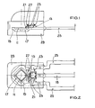
- the optoelectronic receiver shown in FIGS. 1 to 4 has a serving as a photosensitive semiconductor device silicon photodiode 11 and a control circuit 13 on a ground conductor strip 15 arranged of metal, for example, are glued.
- the ground conductor strip 15 Around Photodiode 11, the ground conductor strip 15 has a trough-shaped Recess 17, in which the photodiode 11 is inserted.
- the recess 17 opposite end of the ground conductor strip 15 as a Ground connection legs 19 formed.
- the photodiode 11 and the control circuit 13 are by means of a signal bonding wire 21 connected to each other, wherein the photodiode 11 and the Control circuit 13 are configured such that the signal bonding wire 21 for transmitting the received signals of the photodiode 11 to the Control circuit 13 is used.
- connection legs 25 connect the control circuit 13 with the Ground conductor strips 15 and each with two outer leads 25.
- One of these connection legs 25, for example, for supply Serve the receiver with the operating voltage while the other leads 25 serve as signal output.
- two shielding bonding wires 27 are provided, each on both ends are connected to the ground conductor strip 15 and the cross the signal bonding wire 21.
- the two shielding bonding wires 27 extend in the plan view according to FIGS. 2 and 4 obliquely to the signal bonding wire 21 and parallel to each other.
- connection pins 19, 25 protrude from the housing and ultimately parallel to each other.
- the housing 29 is in the infrared Spectral range, for which the photodiode 11 is also sensitive, transparent.
- the optoelectronic receiver shown in FIGS. 1 to 4 serves as Signal receiver of an infrared remote control.
- the photodiode converts 11 the received in the infrared optical signals into electrical Signals to the first via the signal bonding wire 21 to the control circuit 13 will be forwarded.
- the shielding bonding wires 27 effect an advantageous shielding of the Signal bonding wire 21 against electromagnetic interference, since the shielding bonding wires 27 together with the ground conductor strip 15th form a closed enclosure of the signal bonding wire 21.
- the ground conductor strip 15 is in operation of the optoelectronic receiver on set the electrical ground potential of the receiver. Due to the Over the signal bonding wire 21 by thus also on the Ground potential set Ablebonddrähte 27 are external electromagnetic Interference signals shielded, otherwise unattenuated the guided along the signal-bonding wire 21 useful signal would overlap.
- Another measure for shielding the photodiode 11 against external Electromagnetic interference consists in the arrangement of the photodiode 11 in the trough-like depression 17 of the ground conductor strip 15th
- the bottom and the side walls of the trough-shaped depression 17 suppress the incident from below and from the side noise or at least weaken it.
- Another advantage of the arrangement of Photodiode 11 in the trough-shaped recess 17 is that the signal bonding wire 21 a flat course of the photodiode 11 to the control circuit 13 can take, so that the spread of the Signal bonding wire 21 by means of shielding bonding wires 27 on particular simple way can be realized.
- the photodiode 11 is connected to the in Fig. 2 shown light entrance side with a shielding of a conductive and translucent material provided, for example by means of a further bonding wire or by a corresponding doping profile is also set to the ground potential of the receiver.
- a shielding layer For example, doped polysilicon or ITO (indium tin oxides).
- the shielding layer is by means of an insulating layer, for example, of silicon dioxide, from the active layer of Photodiode 11 separated.
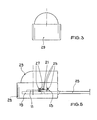
- Fig. 5 shows that the illustrated trough-shaped recess 17 of the ground conductor strip 15 is not mandatory.
- the photodiode 11 and the control circuit 13 instead at the same height on the Ground conductor strips 15 arranged.
- the photodiode 11 and the control circuit 13 are in turn connected by means of the signal bonding wire 21. This is crossed by two shielding bonding wires 27.
Landscapes
- Light Receiving Elements (AREA)
Abstract
Ein insbesondere als Fernsteuer-Empfangsmodul ausgebildeter optoelektronischer Empfänger besitzt ein lichtempfindliches Halbleiterbauelement (11) und einen Steuerschaltkreis (13). Das lichtempfindliche Halbleiterbauelement (11) ist mit dem Steuerschaltkreis (13) zur Übertragung von Empfangssignalen mittels einer Signalleitung (21) verbunden. Der optoelektronische Empfänger weist wenigstens einen Abschirm-Bonddraht (27) auf, der quer zu der Signalleitung (21) verläuft, die Signalleitung (21) übergreift und an beiden Enden mit einem Konstantpotentialanschluss (15) verbunden ist. <IMAGE>
Description
Die Erfindung betrifft einen optoelektronischen Empfänger, insbesondere
ein Fernsteuer-Empfangsmodul, mit einem lichtempfindlichen Halbleiterbauelement
und einem Steuerschaltkreis, wobei zur Übertragung von
Empfangssignalen das lichtempfindliche Halbleiterbauelement mit dem
Steuerschaltkreis mittels einer Signalleitung verbunden ist.
Ein derartiger optoelektronischer Empfänger wird beispielsweise im Zusammenhang
mit Infrarot-Fernsteuerungen eingesetzt, um optische Signale,
die von einem zugeordneten Sender ausgestrahlt werden, innerhalb
des lichtempfindlichen Halbleiterbauelements in photoelektrische Empfangssignale
umzuwandeln. Diese Empfangssignale werden mittels der
Signalleitung an den Steuerschaltkreis weitergeleitet. Dort kann beispielsweise
eine Filterung, Formung, Verstärkung oder Dekodierung der
Empfangssignale oder eine sonstige Steuerung des lichtempfindlichen
Halbleiterbauelements erfolgen.
Da derartige Fernsteuerungen über große Distanzen funktionsfähig sein
sollen und damit sehr empfindlich gegenüber der optischen Strahlung
sein müssen, besteht die Gefahr, dass elektromagnetische Störungen in
die Empfangssignale eingekoppelt werden und diese verfälschen. Derartige
elektromagnetische Störungen können beispielsweise durch Schaltnetzteile
erzeugt werden, die in der Nähe des Empfängers angeordnet sind.
Um derartige Störungen zu unterdrücken, ist es beispielsweise bekannt,
den Empfänger oder zumindest das lichtempfindliche Halbleiterbauelement
mit zusätzlichen Gehäuseteilen aus Metall zu versehen, die auf ein
konstantes elektrisches Potential gelegt werden. Trotz dieser Maßnahme
kann die unerwünschte Beeinflussung durch elektromagnetische Störsignale
nicht immer in dem erwünschten Maß beseitigt werden.
Es ist eine Aufgabe der Erfindung, einen optoelektronischen Empfänger
mit einem lichtempfindlichen Halbleiterbauelement und einem Steuerschaltkreis
noch besser gegen elektromagnetische Störungen zu schützen.
Diese Aufgabe wird durch eine optoelektronischen Empfänger mit den
Merkmalen des Anspruchs 1 gelöst, und insbesondere dadurch, dass der
Empfänger wenigstens einen Abschirm-Bonddraht aufweist, der quer zu
der Signalleitung verläuft, die Signalleitung übergreift und an beiden
Enden mit einem Konstantpotentialanschluss verbunden ist.
Der erfindungsgemäße Empfänger zeichnet sich also dadurch aus, dass
ein oder mehrere Abschirm-Bonddrähte die Signalleitung überqueren, die
zwischen dem lichtempfindlichen Halbleiterbauelement und dem Steuerschaltkreis
verläuft. Der oder die Abschirm-Bonddrähte verlaufen dabei
quer, d.h. senkrecht oder schräg zu der Signalleitung, und sie sind auf ein
konstantes elektrisches Potential gelegt. Hierdurch ist also eine Art Umhüllung
der Signalleitung verwirklicht. Somit ist eine Abschirmung der
mittels der Signalleitung geführten, üblicherweise noch unverstärkten
Empfangssignale gegenüber äußeren elektromagnetischen Störungen
gewährleistet.
Ein besonderer Vorteil besteht darin, dass die mit dem oder den Abschirm-Bonddrähten
verwirklichte zusätzliche Abschirmmaßnahme fertigungstechnisch
auf einfache und somit kostengünstige Weise realisiert
werden kann. Üblicherweise ist nämlich bei einem optoelektronischen
Empfänger ohnehin die Anbringung von Bonddrähten vorgesehen, beispielsweise
um eine Bondverbindung zwischen dem lichtempfindlichen
Halbleiterelement und dem Steuerschaltkreis oder um Bondverbindungen
zwischen diesen Bauelementen und Anschlussbeinchen des Empfängers
herzustellen. Somit können die ohnehin genutzten Fertigungsanlagen
ohne bedeutenden zusätzlichen Aufwand dazu genutzt werden, den oder
die Abschirm-Bonddrähte anzubringen, um die zusätzliche Abschirmung
der Signalleitung zu verwirklichen.
Die Erfindung ist natürlich nicht darauf beschränkt, dass über die Signalleitung
ausschließlich Empfangssignale übertragen werden. Die erläuterten
Vorteile der Erfindung werden vielmehr auch dann verwirklicht, wenn
über die Signalleitung zusätzlich beispielsweise auch die Betriebsspannung
für das lichtempfindliche Halbleiterelement übertragen wird.
Selbstverständlich kann die Erfindung unabhängig davon realisiert werden,
ob das lichtempfindliche Halbleiterbauelement im sichtbaren, im
infraroten oder im ultravioletten Spektralbereich detektiert. Das lichtempfindliche
Halbleiterbauelement kann beispielsweise durch eine Photodiode
oder einen Phototransistor gebildet sein.
Es ist bevorzugt, wenn der Abschirm-Bonddraht gemeinsam mit dem
Konstantpotentialanschluss eine geschlossene Schleife bildet, d.h. wenn
der Konstantpotentialanschluss die beiden Enden des Abschirm-Bonddrahts
direkt miteinander verbindet. Hierdurch ist gewährleistet,
dass die durch den Abschirm-Bonddraht und den Konstantpotentialanschluss
gebildete geschlossene Schleife die Signalleitung umfänglich
umschließt. Hierdurch wird eine besonders gute Abschirmwirkung erzielt.
Weiterhin ist es bevorzugt, wenn der Abschirm-Bonddraht an beiden
Enden mit einem Masse-Leiterstreifen verbunden ist, d.h. einem Leiterstreifen,
der ohnehin zum Aufbau des optoelektronischen Empfängers
dient und der im Betrieb des Empfängers als Massekontakt vorgesehen
ist. Der Leiterstreifen kann beispielsweise als ein als Stanz-/Biegeteil
vorgesehener Metallstreifen oder als ein Platinenabschnitt ausgebildet
sein.
Weitere Ausführungsformen der Erfindung sind in den Unteransprüchen
genannt.
Die Erfindung wird nachfolgend lediglich beispielhaft unter Bezugnahme
auf die Zeichnungen erläutert.
- Fig. 1
- zeigt eine Seitenansicht einer ersten Ausführungsform eines optoelektronischen Empfängers.
- Fig. 2
- zeigt eine Draufsicht der Ausführungsform gemäß Fig. 1.
- Fig. 3
- zeigt eine Vorderansicht des Gehäuses der Ausführungsform gemäß Fig. 1.
- Fig. 4
- zeigt eine Detailansicht der Verbindung von Photodiode und Steuerschaltkreis gemäß Fig. 2.
- Fig. 5
- zeigt eine Seitenansicht einer weiteren Ausführungsform.
Der in den Fig. 1 bis 4 gezeigte optoelektronische Empfänger besitzt eine
als lichtempfindliches Halbleiterbauelement dienende Silizium-Photodiode
11 sowie einen Steuerschaltkreis 13, die auf einem Masse-Leiterstreifen
15 aus Metall angeordnet, beispielsweise aufgeklebt sind. Im Bereich der
Photodiode 11 besitzt der Masse-Leiterstreifen 15 eine wannenförmige
Vertiefung 17, in die die Photodiode 11 eingesetzt ist. An dem der Vertiefung
17 gegenüber liegenden Ende ist der Masse-Leiterstreifen 15 als ein
Masse-Anschlussbeinchen 19 ausgebildet.
Die Photodiode 11 und der Steuerschaltkreis 13 sind mittels eines Signal-Bonddrahts
21 miteinander verbunden, wobei die Photodiode 11 und der
Steuerschaltkreis 13 dergestalt konfiguriert sind, dass der Signal-Bonddraht
21 zur Übertragung der Empfangssignale der Photodiode 11 an den
Steuerschaltkreis 13 dient.
Weitere Bonddrähte 23 verbinden den Steuerschaltkreis 13 mit dem
Masse-Leiterstreifen 15 und jeweils mit zwei äußeren Anschlussbeinchen
25. Eines dieser Anschlussbeinchen 25 kann beispielsweise zur Versorgung
des Empfängers mit der Betriebsspannung dienen, während das
andere Anschlussbeinchen 25 als Signalausgang dient.
Ferner sind zwei Abschirm-Bonddrähte 27 vorgesehen, die jeweils an
beiden Enden mit dem Masse-Leiterstreifen 15 verbunden sind und die
den Signal-Bonddraht 21 überqueren. Die beiden Abschirm-Bonddrähte
27 verlaufen in der Draufsicht gemäß Fig. 2 und 4 schräg zu dem Signal-Bonddraht
21 und parallel zueinander.
Die genannten Bauteile sind in einem gemeinsamen Gehäuse 29 vergossen,
wobei die Anschlussbeinchen 19, 25 aus dem Gehäuse herausragen
und letztlich parallel zueinander verlaufen. Das Gehäuse 29 ist im infraroten
Spektralbereich, für den auch die Photodiode 11 empfindlich ist,
transparent.
Der in den Fig. 1 bis 4 gezeigte optoelektronische Empfänger dient als
Signalempfänger einer Infrarot-Fernsteuerung. Hierfür wandelt die Photodiode
11 die im Infraroten empfangenen optischen Signale in elektrische
Signale um, die über den Signal-Bonddraht 21 zunächst an den Steuerschaltkreis
13 weitergeleitet werden. Dort erfolgt eine erste Signalverarbeitung,
insbesondere eine Signalfilterung und -verstärkung. Anschließend
werden die derartig vorverarbeiteten Empfangssignale über ein Anschlussbeinchen
25 des Empfängers ausgegeben.
Die Abschirm-Bonddrähte 27 bewirken eine vorteilhafte Abschirmung des
Signal-Bonddrahts 21 gegenüber elektromagnetischen Störsignalen, da
die Abschirm-Bonddrähte 27 gemeinsam mit dem Masse-Leiterstreifen 15
eine geschlossene Umhüllung des Signal-Bonddrahts 21 bilden. Der Masse-Leiterstreifen
15 ist im Betrieb des optoelektronischen Empfängers auf
das elektrische Massepotential des Empfängers gesetzt. Aufgrund des
Übergreifens des Signal-Bonddrahts 21 durch die somit ebenfalls auf das
Massepotential gesetzten Abschirmbonddrähte 27 werden externe elektromagnetische
Störsignale abgeschirmt, die sich anderenfalls ungeschwächt
dem entlang des Signal-Bonddrahts 21 geführten Nutzsignal
überlagern würden.
Diese vorteilhafte Abschirmungsmaßnahme kann fertigungstechnisch auf
sehr einfache Weise verwirklicht werden, da bei der Herstellung des gezeigten
Empfängers ohnehin Bonddrähte 21, 23 angebracht werden müssen.
Das zusätzliche Anbringen der Abschirm-Bonddrähte 27 bedeutet
demgegenüber keinen erheblichen Mehraufwand.
Eine weitere Maßnahme zur Abschirmung der Photodiode 11 gegen externe
elektromagnetische Störsignale besteht in der Anordnung der Photodiode
11 in der wannenartigen Vertiefung 17 des Masse-Leiterstreifens 15.
Der Boden und die Seitenwände der wannenförmigen Vertiefung 17 unterdrücken
die von unten und von der Seite einfallende Störstrahlung oder
schwächen diese zumindest ab. Ein weiterer Vorteil der Anordnung der
Photodiode 11 in der wannenförmigen Vertiefung 17 besteht darin, dass
der Signal-Bonddraht 21 einen flachen Verlauf von der Photodiode 11 zu
dem Steuerschaltkreis 13 einnehmen kann, so dass das Übergreifen des
Signal-Bonddrahts 21 mittels der Abschirm-Bonddrähte 27 auf besonders
einfache Weise verwirklicht werden kann.
Gemäß einer vorteilhaften Weiterbildung ist die Photodiode 11 an der in
Fig. 2 gezeigten Lichteintrittsseite mit einer Abschirmschicht aus einem
leitfähigen und lichtdurchlässigen Material versehen, die beispielsweise
mittels eines weiteren Bonddrahts oder durch ein entsprechendes Dotierungsprofil
ebenfalls auf das Massepotential des Empfängers gesetzt ist.
Hierdurch wird die Photodiode 11 auch gegen von oben einfallende elektromagnetische
Störungen abgeschirmt. Die genannte Abschirmschicht
kann beispielsweise aus dotiertem Polysilizium oder aus ITO (indium tin
oxide) bestehen. Vorzugsweise ist die Abschirmschicht mittels einer Isolierschicht,
beispielsweise aus Siliziumdioxid, von der aktiven Schicht der
Photodiode 11 getrennt.
Fig. 5 zeigt, dass die erläuterte wannenförmige Vertiefung 17 des Masse-Leiterstreifens
15 nicht zwingend erforderlich ist. Hier sind die Photodiode
11 und der Steuerschaltkreis 13 stattdessen auf gleicher Höhe auf dem
Masse-Leiterstreifen 15 angeordnet. Die Photodiode 11 und der Steuerschaltkreis
13 sind wiederum mittels des Signal-Bonddrahts 21 verbunden.
Dieser wird von zwei Abschirm-Bonddrähten 27 überquert.
- 11
- Photodiode
- 13
- Steuerschaltkreis
- 15
- Masse-Leiterstreifen
- 17
- Vertiefung
- 19
- Masse-Anschlussbeinchen
- 21
- Signal-Bonddraht
- 23
- Bonddraht
- 25
- Anschlussbeinchen
- 27
- Abschirm-Bonddraht
- 29
- Gehäuse
Claims (10)
- Optoelektronischer Empfänger, insbesondere Fernsteuer-Empfangsmodul,
mit einem lichtempfindlichen Halbleiterbauelement (11) und einem Steuerschaltkreis (13),
wobei das lichtempfindliche Halbleiterbauelement mit dem Steuerschaltkreis zur Übertragung von Empfangssignalen mittels einer Signalleitung (21) verbunden ist,
dadurch gekennzeichnet, dass der optoelektronische Empfänger wenigstens einen Abschirm-Bonddraht (27) aufweist, der quer zu der Signalleitung (21) verläuft, die Signalleitung übergreift und an beiden Enden mit einem Konstantpotentialanschluss (15) verbunden ist. - Optoelektronischer Empfänger nach Anspruch 1,
dadurch gekennzeichnet, dass der Abschirm-Bonddraht (27) mit dem Konstantpotentialanschluss (15) eine geschlossene Schleife bildet, die die Signalleitung (21) umschließt. - Optoelektronischer Empfänger nach einem der vorhergehenden Ansprüche,
dadurch gekennzeichnet, dass der Abschirm-Bonddraht (27) an beiden Enden mit einem Masse-Leiterstreifen (15) verbunden ist. - Optoelektronischer Empfänger nach Anspruch 3,
dadurch gekennzeichnet, dass das lichtempfindliche Halbleiterbauelement (11) und der Steuerschaltkreis (13) auf dem Masse-Leiterstreifen (15) angeordnet sind. - Optoelektronischer Empfänger nach einem der Ansprüche 3 oder 4,
dadurch gekennzeichnet, dass an dem Masse-Leiterstreifen (15) eine wannenförmige Vertiefung (17) ausgebildet ist, und
dass das lichtempfindliche Halbleiterbauelement (11) in der Vertiefung (17) angeordnet ist. - Optoelektronischer Empfänger nach einem der vorhergehenden Ansprüche,
dadurch gekennzeichnet, dass der optoelektronische Empfänger mehrere Abschirm-Bonddrähte (27) aufweist. - Optoelektronischer Empfänger nach einem der vorhergehenden Ansprüche,
dadurch gekennzeichnet, dass die Signalleitung (21) durch einen Bonddraht gebildet ist. - Optoelektronischer Empfänger nach einem der vorhergehenden Ansprüche,
dadurch gekennzeichnet, dass das lichtempfindliche Halbleiterbauelement (11) an der Lichteintrittsseite mit einer Abschirmschicht aus einem leitfähigen und lichtdurchlässigen Material versehen ist. - Optoelektronischer Empfänger nach einem der vorhergehenden Ansprüche,
dadurch gekennzeichnet, dass das lichtempfindliche Halbleiterbauelement (11), der Steuerschaltkreis (13), die Signalleitung (21) und der Abschirm-Bonddraht (27) in einem gemeinsamen transparenten Gehäuse (29) vergossen sind. - Optoelektronischer Empfänger nach einem der vorhergehenden Ansprüche,
dadurch gekennzeichnet, dass das lichtempfindliche Halbleiterbauelement (11) im infraroten Wellenlängenbereich empfindlich ist,
und/oder
dass das lichtempfindliche Halbleiterbauelement (11) durch eine Photodiode oder einen Phototransistor gebildet ist.
Priority Applications (1)
| Application Number | Priority Date | Filing Date | Title |
|---|---|---|---|
| EP04010489A EP1594162A1 (de) | 2004-05-03 | 2004-05-03 | Optoelektronischer Empfänger |
Applications Claiming Priority (1)
| Application Number | Priority Date | Filing Date | Title |
|---|---|---|---|
| EP04010489A EP1594162A1 (de) | 2004-05-03 | 2004-05-03 | Optoelektronischer Empfänger |
Publications (1)
| Publication Number | Publication Date |
|---|---|
| EP1594162A1 true EP1594162A1 (de) | 2005-11-09 |
Family
ID=34924835
Family Applications (1)
| Application Number | Title | Priority Date | Filing Date |
|---|---|---|---|
| EP04010489A Withdrawn EP1594162A1 (de) | 2004-05-03 | 2004-05-03 | Optoelektronischer Empfänger |
Country Status (1)
| Country | Link |
|---|---|
| EP (1) | EP1594162A1 (de) |
Cited By (2)
| Publication number | Priority date | Publication date | Assignee | Title |
|---|---|---|---|---|
| WO2008074446A1 (de) * | 2006-12-16 | 2008-06-26 | Atmel Germany Gmbh | Halbleiterbauelement |
| CN119805684A (zh) * | 2019-05-09 | 2025-04-11 | 苏州旭创科技有限公司 | 光学组件及具有其的光模块 |
Citations (3)
| Publication number | Priority date | Publication date | Assignee | Title |
|---|---|---|---|---|
| EP0202109A2 (de) * | 1985-05-13 | 1986-11-20 | Kabushiki Kaisha Toshiba | Halbleiteranordnung mit hohem Widerstand gegen elektrostatische und elektromagnetische Induktion |
| DE4212948A1 (de) * | 1992-04-18 | 1993-10-21 | Telefunken Microelectron | Halbleiterbaugruppe, insbesondere Fernsteuer-Empfangsmodul |
| EP0624962A2 (de) * | 1993-04-09 | 1994-11-17 | Sumitomo Electric Industries, Ltd. | Optisches Modul |
-
2004
- 2004-05-03 EP EP04010489A patent/EP1594162A1/de not_active Withdrawn
Patent Citations (3)
| Publication number | Priority date | Publication date | Assignee | Title |
|---|---|---|---|---|
| EP0202109A2 (de) * | 1985-05-13 | 1986-11-20 | Kabushiki Kaisha Toshiba | Halbleiteranordnung mit hohem Widerstand gegen elektrostatische und elektromagnetische Induktion |
| DE4212948A1 (de) * | 1992-04-18 | 1993-10-21 | Telefunken Microelectron | Halbleiterbaugruppe, insbesondere Fernsteuer-Empfangsmodul |
| EP0624962A2 (de) * | 1993-04-09 | 1994-11-17 | Sumitomo Electric Industries, Ltd. | Optisches Modul |
Cited By (2)
| Publication number | Priority date | Publication date | Assignee | Title |
|---|---|---|---|---|
| WO2008074446A1 (de) * | 2006-12-16 | 2008-06-26 | Atmel Germany Gmbh | Halbleiterbauelement |
| CN119805684A (zh) * | 2019-05-09 | 2025-04-11 | 苏州旭创科技有限公司 | 光学组件及具有其的光模块 |
Similar Documents
| Publication | Publication Date | Title |
|---|---|---|
| EP1174745B1 (de) | Optoelektronisches oberflächenmontierbares Modul | |
| DE102004061930B4 (de) | Optisches Halbleiterbauelement zur Ankopplung an eine optische Faser und damit ausgerüstete elektronische Einrichtung | |
| EP0566921B1 (de) | Halbleiterbaugruppe, insbesondere Fernsteuer-Empfangsmodul | |
| DE102017130065B4 (de) | Sensorvorrichtung | |
| DE102005008323A1 (de) | Optische Halbleitervorrichtung und diese verwendende elektronische Anordnung | |
| DE102013114547A1 (de) | TO-Gehäuse sowie Verfahren zu dessen Herstellung | |
| WO2011079896A1 (de) | Sensor mit gehäuse und verfahren zu dessen herstellung | |
| DE19923960A1 (de) | Infrarotsensor | |
| DE19649650A1 (de) | Strahlungsemittierendes Halbleiterbauelement | |
| US7348551B2 (en) | Remote-control light receiving unit and electronic apparatus using the same | |
| EP1594162A1 (de) | Optoelektronischer Empfänger | |
| EP1249044B1 (de) | Optische sende- und empfangseinrichtung und deren herstellungsverfahren | |
| DE102005047170A1 (de) | Optische Vorrichtung, optischer Verbinder und damit ausgerüstete elektronische Einrichtung | |
| DE69838045T2 (de) | Optischer Empfänger mit Schutzvorrichtungen gegen elektromagnetisches Rauschen | |
| DE60036762T2 (de) | Lichtkoppler | |
| DE102013102714A1 (de) | Hochfrequenzdurchführung | |
| DE112010002553T5 (de) | Modul zur optischen kommunikation | |
| EP1665307A2 (de) | Anordnung zur überwachung elektrischer einrichtungen auf störlichtbögen | |
| EP2015033A1 (de) | Sensor | |
| EP1594167B1 (de) | Optoelektronischer Empfänger | |
| EP3355075A1 (de) | Sensoranordnung | |
| DE3824000C2 (de) | ||
| EP1608026A2 (de) | Optoelektronische Vorrichtung und Verfahren zur Herstellung einer optoelektronischen Vorrichtung | |
| DE19948457C2 (de) | Optoelektronische Baugruppe | |
| DE10134585C1 (de) | Kommunikations-Endgerät mit optischer Signalübertragung |
Legal Events
| Date | Code | Title | Description |
|---|---|---|---|
| PUAI | Public reference made under article 153(3) epc to a published international application that has entered the european phase |
Free format text: ORIGINAL CODE: 0009012 |
|
| AK | Designated contracting states |
Kind code of ref document: A1 Designated state(s): AT BE BG CH CY CZ DE DK EE ES FI FR GB GR HU IE IT LI LU MC NL PL PT RO SE SI SK TR |
|
| AX | Request for extension of the european patent |
Extension state: AL HR LT LV MK |
|
| AKX | Designation fees paid | ||
| STAA | Information on the status of an ep patent application or granted ep patent |
Free format text: STATUS: THE APPLICATION IS DEEMED TO BE WITHDRAWN |
|
| 18D | Application deemed to be withdrawn |
Effective date: 20060510 |
|
| REG | Reference to a national code |
Ref country code: DE Ref legal event code: 8566 |