EP1594193A1 - Dispositif de contact - Google Patents
Dispositif de contact Download PDFInfo
- Publication number
- EP1594193A1 EP1594193A1 EP05004518A EP05004518A EP1594193A1 EP 1594193 A1 EP1594193 A1 EP 1594193A1 EP 05004518 A EP05004518 A EP 05004518A EP 05004518 A EP05004518 A EP 05004518A EP 1594193 A1 EP1594193 A1 EP 1594193A1
- Authority
- EP
- European Patent Office
- Prior art keywords
- contact
- tip
- leading
- inclined surface
- leg
- Prior art date
- Legal status (The legal status is an assumption and is not a legal conclusion. Google has not performed a legal analysis and makes no representation as to the accuracy of the status listed.)
- Granted
Links
- 238000003780 insertion Methods 0.000 claims abstract description 14
- 230000037431 insertion Effects 0.000 claims abstract description 14
- 230000013011 mating Effects 0.000 claims description 13
- 239000004020 conductor Substances 0.000 claims description 8
- 238000011144 upstream manufacturing Methods 0.000 claims description 3
- 230000007704 transition Effects 0.000 claims description 2
- 230000001154 acute effect Effects 0.000 abstract 1
- 210000002414 leg Anatomy 0.000 description 22
- 239000004973 liquid crystal related substance Substances 0.000 description 6
- 230000000694 effects Effects 0.000 description 3
- 238000003892 spreading Methods 0.000 description 3
- 230000007480 spreading Effects 0.000 description 3
- 238000004519 manufacturing process Methods 0.000 description 2
- 238000000034 method Methods 0.000 description 2
- 238000004080 punching Methods 0.000 description 2
- IUYHQGMDSZOPDZ-UHFFFAOYSA-N 2,3,4-trichlorobiphenyl Chemical compound ClC1=C(Cl)C(Cl)=CC=C1C1=CC=CC=C1 IUYHQGMDSZOPDZ-UHFFFAOYSA-N 0.000 description 1
- 230000009471 action Effects 0.000 description 1
- 238000005452 bending Methods 0.000 description 1
- 230000008901 benefit Effects 0.000 description 1
- 239000011248 coating agent Substances 0.000 description 1
- 238000000576 coating method Methods 0.000 description 1
- 238000006073 displacement reaction Methods 0.000 description 1
- PCHJSUWPFVWCPO-UHFFFAOYSA-N gold Chemical compound [Au] PCHJSUWPFVWCPO-UHFFFAOYSA-N 0.000 description 1
- 239000010931 gold Substances 0.000 description 1
- 229910052737 gold Inorganic materials 0.000 description 1
- 230000001771 impaired effect Effects 0.000 description 1
- 238000009413 insulation Methods 0.000 description 1
- 230000003993 interaction Effects 0.000 description 1
- 230000007774 longterm Effects 0.000 description 1
- 230000008569 process Effects 0.000 description 1
- 238000005096 rolling process Methods 0.000 description 1
- 238000004513 sizing Methods 0.000 description 1
- 210000000689 upper leg Anatomy 0.000 description 1
Images


Classifications
-
- H—ELECTRICITY
- H01—ELECTRIC ELEMENTS
- H01R—ELECTRICALLY-CONDUCTIVE CONNECTIONS; STRUCTURAL ASSOCIATIONS OF A PLURALITY OF MUTUALLY-INSULATED ELECTRICAL CONNECTING ELEMENTS; COUPLING DEVICES; CURRENT COLLECTORS
- H01R13/00—Details of coupling devices of the kinds covered by groups H01R12/70 or H01R24/00 - H01R33/00
- H01R13/02—Contact members
- H01R13/10—Sockets for co-operation with pins or blades
- H01R13/11—Resilient sockets
- H01R13/112—Resilient sockets forked sockets having two legs
-
- H—ELECTRICITY
- H01—ELECTRIC ELEMENTS
- H01R—ELECTRICALLY-CONDUCTIVE CONNECTIONS; STRUCTURAL ASSOCIATIONS OF A PLURALITY OF MUTUALLY-INSULATED ELECTRICAL CONNECTING ELEMENTS; COUPLING DEVICES; CURRENT COLLECTORS
- H01R12/00—Structural associations of a plurality of mutually-insulated electrical connecting elements, specially adapted for printed circuits, e.g. printed circuit boards [PCB], flat or ribbon cables, or like generally planar structures, e.g. terminal strips, terminal blocks; Coupling devices specially adapted for printed circuits, flat or ribbon cables, or like generally planar structures; Terminals specially adapted for contact with, or insertion into, printed circuits, flat or ribbon cables, or like generally planar structures
- H01R12/70—Coupling devices
- H01R12/71—Coupling devices for rigid printing circuits or like structures
- H01R12/72—Coupling devices for rigid printing circuits or like structures coupling with the edge of the rigid printed circuits or like structures
- H01R12/721—Coupling devices for rigid printing circuits or like structures coupling with the edge of the rigid printed circuits or like structures cooperating directly with the edge of the rigid printed circuits
Definitions
- MID "Molded Interconnect Devices "”
- the Contact device associated with the mating contacts Marginal edges to sliding contacts such as fork spring contacts, Double leg flat springs od.
- the Legs of the fork springs so asymmetrically form that the liquid crystal display at first obliquely to the opening of Fork springs without overcoming a spring force is to introduce and then by tilting to the parallel of the longitudinal axis of Fork springs whose two legs for two-sided contacting in the connector strip expands.
- Object of the present invention is essentially a To provide contact device of the type assumed to be known, which are simply designed and protected against damage Contact surfaces is particularly protected.
- the invention solves this problem with the features of Claim 1 and is accordingly characterized in that the respective muzzle inclined surface in an additional contact tip goes over, the contact tip in the direction of the contact as leading contact point is upstream.
- the essential core of the invention is accordingly provide additional contact points that possibly contact damaging influence of mating contacts, in particular eliminate their sharp or rugged edges or at least "defuse" before the conductive parts of the mating contacts with the actual contact blades come into operative contact.
- DE 1 046 137 proposes for each contact unit two or more adjacent contact elements to provide, wherein the contact-making crests of the contact elements are arranged offset in the insertion direction such that when Insert the printed circuit the contact elements each Contact one after the other.
- Everybody exists here Contact device of at least two, preferably three side by side lying fork-shaped contact elements, each in opposing arrangement a Kunststoffkuppencru exhibit.
- additional contact points present, but not in the sense of the invention the actual Contact tip upstream in the direction of insertion of the contact leading.
- the mouth inclined surface each have a steep Angle (W) of about 40 ° to 55 ° to the direction of insertion includes and that the transition from the leading contact point to the actual The contact tip is flatter than the mouth slope and in each case an angle (W) of about 15 ° to 30 ° to the direction of insertion includes.
- W steep Angle
- existing muzzle slopes are these according to the invention by special steepness "aggressive" designed to get as close as possible to the target, disturbing burrs, Edges od. The like. To settle the mating contact elements.
- highly miniaturized contact device preferably all contact points with the contact in one piece as well formed material-material-cohesive.
- the invention provides an embodiment in which the leading contact tip of a contact leg with respect to the leading contact point of the other contact leg in the insertion direction arranged offset by a certain amount.
- one Contact element according to the invention differs, apart from only the geometric shape of the generating Tool, not from the production of a usual simple Fork spring contact. Consequently, the invention requires virtually no additional effort and costs.
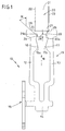
- a total of 10 designated contact device comprises a number of contact springs 11, which are used as fork springs Fork legs 12 and 13 and a connecting them Fork 14 are formed. At the latter is a foot part or Conductor connection portion 15 in particular material-material-cohesive tethered. This can be a Crimp connection act for stripped conductor ends, but also e.g. around an insulation displacement fork. Otherwise, section 15 is not Subject of the present invention.
- Each of the two fork legs 12, 13 has at its for facing each fork legs 13 and 12, respectively Page a so-called contact point 16 or 17 on.
- the offset 19 reduce the insertion force due to the time lag of the maximum deflection of the fork legs 12 and 13 during a Plugging process.
- the fork spring contact 11 is perpendicular to the plane from a flat rectangular contact sheet cut out.
- the contact tops 16 and 17 make their contact surfaces with the punching surfaces 16a and 17a ready.
- these contact surfaces 16a and 17a, possibly also the entire contact spring 11, are in terms of optimal electrical contact enhanced by a galvanic coating such as. a tinning or gilding.
- This finishing layer is very sensitive and can, for example, by sharp edges 24 be damaged by mating contacts 20.
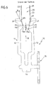
- Fig. 6 are therefore the marginal edges of a circuit board 20th by training two bevels 31 a little "defused". nevertheless still remain from Fig. 6 apparent, despite the chamfer 31st sharp edges 24 are left as possibly damaging.
- This contact device 10 or the contact spring 11 is now in specially designed to work even with sharp edges 24, 25 of Mating contacts 20 such. a printed circuit board 21 with conductor tracks 22 and 23, to be contacted without the contact surfaces 16a, 17a or their finishing layers suffer damage.
- each of the two fork legs 12 and 13 each have another, so-called leading contact point 29 and 30 are provided.
- Their inner surfaces are 29a and 30a designated.
- the Contact tips 29 and 30 and thus also their inner surfaces 29a and 30a have a longitudinal offset, which in FIG. 1 denotes 28 is.
- At the leading contact points 29 and 30 close to free end of the fork legs 12 and 13 each one Muzzle inclined surface 26 and 27 at.
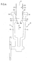
- the mouth inclined surface 27 has now the now smoothed edge 25 leave. Meanwhile, the opposite edge 24 of the circuit board 21 a piece along the along opposite mouth slope 26 slid along and has smoothed these too. At the same time, the force contact between the edge 24 and the mouth inclined surface 26 the Fork leg 12 and 13 further spread.
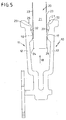
- Fig. 3 is on the one hand to see that the edges 24 and 25 of the Circuit board 21 have been chamfered and that now the circuit board 21 between the two mouth inclined surfaces 26 and 27 of the Contact device 10 is located.
- the Printed circuit board edge 24 In the further course of the attachment of the contact device 10th touched on the circuit board 21, as shown in Fig. 4, the Printed circuit board edge 24, the one inclined surface 32 (for clarity shown in Fig. 3) between the leading contact tip 29th and the actual contact tip 16 is formed and a Inclination of about 15 ° (angle w in Fig. 3).
- the contact of the PCB edge 24 with the inclined surface 32 optionally leads to further sizing her edge 24.
- the essence is the invention therein, the actual contact caps 16 and 17 for free end of the fork legs 12 and 13 towards so-called leading Preceding contact 29 and 30, which, in particular in Interaction with the previously arranged aggressive Mündungsschräg vom 26 and 27, the edges 24 and 25 of the Mating contact 20, e.g. a circuit board 21, a blade contact or an MID break or settle or chamfer.
Landscapes
- Coupling Device And Connection With Printed Circuit (AREA)
- Connector Housings Or Holding Contact Members (AREA)
Applications Claiming Priority (2)
| Application Number | Priority Date | Filing Date | Title |
|---|---|---|---|
| DE102004021529 | 2004-05-03 | ||
| DE102004021529A DE102004021529B4 (de) | 2004-05-03 | 2004-05-03 | Kontaktvorrichtung |
Publications (2)
| Publication Number | Publication Date |
|---|---|
| EP1594193A1 true EP1594193A1 (fr) | 2005-11-09 |
| EP1594193B1 EP1594193B1 (fr) | 2011-12-14 |
Family
ID=34934012
Family Applications (1)
| Application Number | Title | Priority Date | Filing Date |
|---|---|---|---|
| EP05004518A Expired - Lifetime EP1594193B1 (fr) | 2004-05-03 | 2005-03-02 | Dispositif de contact |
Country Status (5)
| Country | Link |
|---|---|
| US (1) | US7229321B2 (fr) |
| EP (1) | EP1594193B1 (fr) |
| CN (1) | CN100365871C (fr) |
| AT (1) | ATE537581T1 (fr) |
| DE (1) | DE102004021529B4 (fr) |
Cited By (2)
| Publication number | Priority date | Publication date | Assignee | Title |
|---|---|---|---|---|
| ITTO20090849A1 (it) * | 2009-11-04 | 2011-05-05 | Tyco Electronics Amp Italia Srl | Dispositivo retrofit per una lampada led a bulbo |
| WO2013156379A1 (fr) * | 2012-04-16 | 2013-10-24 | Tyco Electronics Amp Gmbh | Ensemble de contact pourvu d'au moins deux bras de contact et agencement de contact comprenant un ensemble de contact pourvu d'au moins deux bras de contact |
Families Citing this family (16)
| Publication number | Priority date | Publication date | Assignee | Title |
|---|---|---|---|---|
| JP5162338B2 (ja) * | 2008-06-09 | 2013-03-13 | モレックス インコーポレイテド | カードエッジコネクタ |
| US20100178814A1 (en) * | 2009-01-12 | 2010-07-15 | David Bryer | Electrical terminal |
| US8556666B2 (en) * | 2011-10-14 | 2013-10-15 | Delphi Technologies, Inc. | Tuning fork electrical contact with prongs having non-rectangular shape |
| DE102012103215B4 (de) | 2012-04-13 | 2015-08-20 | Wago Verwaltungsgesellschaft Mbh | Steckverbinderset |
| CN104704682B (zh) * | 2012-08-22 | 2017-03-22 | 安费诺有限公司 | 高频电连接器 |
| DE202012008961U1 (de) * | 2012-09-17 | 2012-10-12 | Rosenberger Hochfrequenztechnik Gmbh & Co. Kg | Kontaktelement |
| JP5481595B1 (ja) | 2013-08-20 | 2014-04-23 | イリソ電子工業株式会社 | 電気コネクタ |
| DE102014213079B4 (de) * | 2014-07-04 | 2021-10-07 | Röchling Automotive SE & Co. KG | Elektrischer Steckkontakt mit leitfähigem Kunststoff und verringertem Kontaktwiderstand |
| US9989990B2 (en) * | 2014-12-18 | 2018-06-05 | Dell Prodcuts L.P. | Connector with staggered electrical pins |
| CN205178083U (zh) * | 2015-11-10 | 2016-04-20 | 连展科技(深圳)有限公司 | 插头端子 |
| DE102015119473A1 (de) * | 2015-11-11 | 2017-05-11 | Phoenix Contact Gmbh & Co. Kg | Steckkontakt |
| DE102019116332B4 (de) * | 2019-06-17 | 2024-05-23 | Lisa Dräxlmaier GmbH | Elektrischer gabelkontakt mit fixierabschnitt sowie stanzgitter und steckkontaktanordnung |
| US10971863B1 (en) * | 2019-09-25 | 2021-04-06 | Greenconn Corp. | High speed connector assembly and electrical connector thereof |
| US12322890B2 (en) * | 2020-06-29 | 2025-06-03 | Microsoft Technology Licensing, Llc | Systems and methods for improving safety on electronic device connections |
| CN113131298B (zh) * | 2021-04-21 | 2023-02-28 | 立臻科技(昆山)有限公司 | 一种连接器及连接器组件 |
| CN113571934A (zh) * | 2021-08-17 | 2021-10-29 | 长春捷翼汽车零部件有限公司 | 插接端子、插接结构及机动车辆 |
Citations (3)
| Publication number | Priority date | Publication date | Assignee | Title |
|---|---|---|---|---|
| FR1392205A (fr) | 1964-04-22 | 1965-03-12 | Contact électrique à fourche | |
| US3858957A (en) | 1973-08-27 | 1975-01-07 | Amp Inc | Electrical connecting members requiring lower insertion and retraction forces and providing for low contact wear |
| DE3023614C2 (de) | 1980-06-24 | 1987-03-19 | Hans Dipl.-Ing. 8300 Landshut Rilling | Steckerleiste für Flüssigkristallanzeigen |
Family Cites Families (11)
| Publication number | Priority date | Publication date | Assignee | Title |
|---|---|---|---|---|
| DE1046137B (de) * | 1957-04-30 | 1958-12-11 | Gustav Bach | Elektrische Kontaktvorrichtung fuer gedruckte Schaltungen |
| US3040291A (en) * | 1961-05-04 | 1962-06-19 | Methode Electronics Inc | Electric connector socket |
| US3262082A (en) * | 1963-10-10 | 1966-07-19 | Schjeldahl Co G T | Electrical connector for printed circuit board |
| DE1490763A1 (de) * | 1968-03-23 | 1969-06-12 | Ulrich Tuchel | Kontaktvorrichtung |
| US3631381A (en) * | 1970-04-02 | 1971-12-28 | Ind Electronic Hardware Corp | Multiple electrical connector |
| US4106841A (en) * | 1977-03-11 | 1978-08-15 | Bunker Ramo Corporation | Electrical connector for printed circuit boards |
| US5082459A (en) * | 1990-08-23 | 1992-01-21 | Amp Incorporated | Dual readout simm socket |
| US6254435B1 (en) * | 1999-06-01 | 2001-07-03 | Molex Incorporated | Edge card connector for a printed circuit board |
| JP3343578B2 (ja) * | 1999-08-19 | 2002-11-11 | ケル株式会社 | ケーブルコネクタおよびケーブルコネクタ用コンタクト |
| DE10031991B4 (de) * | 2000-06-30 | 2004-02-05 | Valeo Klimasysteme Gmbh | Luftklappe |
| US6764345B1 (en) * | 2003-05-27 | 2004-07-20 | Tyco Electronics Corporation | Electrical card edge connector with dual shorting contacts |
-
2004
- 2004-05-03 DE DE102004021529A patent/DE102004021529B4/de not_active Expired - Fee Related
-
2005
- 2005-03-02 AT AT05004518T patent/ATE537581T1/de active
- 2005-03-02 EP EP05004518A patent/EP1594193B1/fr not_active Expired - Lifetime
- 2005-04-07 CN CNB2005100648424A patent/CN100365871C/zh not_active Expired - Fee Related
- 2005-05-03 US US11/124,919 patent/US7229321B2/en not_active Expired - Fee Related
Patent Citations (3)
| Publication number | Priority date | Publication date | Assignee | Title |
|---|---|---|---|---|
| FR1392205A (fr) | 1964-04-22 | 1965-03-12 | Contact électrique à fourche | |
| US3858957A (en) | 1973-08-27 | 1975-01-07 | Amp Inc | Electrical connecting members requiring lower insertion and retraction forces and providing for low contact wear |
| DE3023614C2 (de) | 1980-06-24 | 1987-03-19 | Hans Dipl.-Ing. 8300 Landshut Rilling | Steckerleiste für Flüssigkristallanzeigen |
Cited By (2)
| Publication number | Priority date | Publication date | Assignee | Title |
|---|---|---|---|---|
| ITTO20090849A1 (it) * | 2009-11-04 | 2011-05-05 | Tyco Electronics Amp Italia Srl | Dispositivo retrofit per una lampada led a bulbo |
| WO2013156379A1 (fr) * | 2012-04-16 | 2013-10-24 | Tyco Electronics Amp Gmbh | Ensemble de contact pourvu d'au moins deux bras de contact et agencement de contact comprenant un ensemble de contact pourvu d'au moins deux bras de contact |
Also Published As
| Publication number | Publication date |
|---|---|
| CN100365871C (zh) | 2008-01-30 |
| ATE537581T1 (de) | 2011-12-15 |
| EP1594193B1 (fr) | 2011-12-14 |
| DE102004021529B4 (de) | 2007-02-01 |
| US7229321B2 (en) | 2007-06-12 |
| DE102004021529A1 (de) | 2005-12-01 |
| CN1694308A (zh) | 2005-11-09 |
| US20050245144A1 (en) | 2005-11-03 |
Similar Documents
| Publication | Publication Date | Title |
|---|---|---|
| EP1594193B1 (fr) | Dispositif de contact | |
| DE69300865T3 (de) | Elektrischer verbinder mit blech als steckkontaktmaterial. | |
| EP2866306B1 (fr) | Prise de contact pour un connecteur à fiches électrique | |
| EP3446366B1 (fr) | Contact enfichable | |
| DE2621984A1 (de) | Kontaktfederleiste | |
| EP2255412A2 (fr) | Dispositif de connexion électrique | |
| DE69606016T2 (de) | Koaxialverbinder und dessen befestigungsmethode auf eine leiterplatte | |
| DE102006012722B3 (de) | Einpress-Kontakt | |
| DE68923016T2 (de) | Elektrischer Endstückstift mit nachgiebigem Teil. | |
| EP3375048B1 (fr) | Contact à enficher | |
| DE69603318T2 (de) | Vorrichtung für elektrische Kontakte mit Isolationsverschiebung | |
| DE4111054C2 (fr) | ||
| EP3000153A1 (fr) | Cavalier enfichable comprenant des éléments en tôle superposés | |
| DE102009019699A1 (de) | Anschlussklemme für Leiterplatten | |
| EP3375047B1 (fr) | Contact à insérer et méthode de fabrication d'un contact à insérer | |
| DE1765989B2 (de) | Steckverbinder für die Aufnahme einer mit Kontaktflächen versehenen Druckschaltungskarte | |
| DE4400702C2 (de) | Einstückige Steckervorrichtung | |
| DE69606032T2 (de) | Artikelzweckdienlich zur markierung und verfahren zur markierung davon | |
| DE102007035325A1 (de) | Stiftförmiges Kontaktelement und Steckverbindung | |
| EP0921597B1 (fr) | Ressort de contact | |
| DE202016106423U1 (de) | Steckverbindung aus Kontaktstift- und Kontaktbuchse, Kontaktstift Kombination aus Stiftleiste und Buchsenleiste | |
| DE202004006998U1 (de) | Kontaktvorrichtung | |
| EP3477783B1 (fr) | Douille de contact pour un connecteur enfichable électrique | |
| DE1963313B2 (de) | Klemmelement zum loetfreien anschluss isolierter elektrischer leiter | |
| DE20014025U1 (de) | Elektrische Anschluß- oder Verbindungseinrichtung |
Legal Events
| Date | Code | Title | Description |
|---|---|---|---|
| PUAI | Public reference made under article 153(3) epc to a published international application that has entered the european phase |
Free format text: ORIGINAL CODE: 0009012 |
|
| AK | Designated contracting states |
Kind code of ref document: A1 Designated state(s): AT BE BG CH CY CZ DE DK EE ES FI FR GB GR HU IE IS IT LI LT LU MC NL PL PT RO SE SI SK TR |
|
| AX | Request for extension of the european patent |
Extension state: AL BA HR LV MK YU |
|
| 17P | Request for examination filed |
Effective date: 20060403 |
|
| AKX | Designation fees paid |
Designated state(s): AT BE BG CH CY CZ DE DK EE ES FI FR GB GR HU IE IS IT LI LT LU MC NL PL PT RO SE SI SK TR |
|
| RAP1 | Party data changed (applicant data changed or rights of an application transferred) |
Owner name: LUMBERG CONNECT GMBH |
|
| 17Q | First examination report despatched |
Effective date: 20100126 |
|
| GRAP | Despatch of communication of intention to grant a patent |
Free format text: ORIGINAL CODE: EPIDOSNIGR1 |
|
| GRAS | Grant fee paid |
Free format text: ORIGINAL CODE: EPIDOSNIGR3 |
|
| GRAA | (expected) grant |
Free format text: ORIGINAL CODE: 0009210 |
|
| AK | Designated contracting states |
Kind code of ref document: B1 Designated state(s): AT BE BG CH CY CZ DE DK EE ES FI FR GB GR HU IE IS IT LI LT LU MC NL PL PT RO SE SI SK TR |
|
| REG | Reference to a national code |
Ref country code: GB Ref legal event code: FG4D Free format text: NOT ENGLISH |
|
| REG | Reference to a national code |
Ref country code: CH Ref legal event code: EP |
|
| REG | Reference to a national code |
Ref country code: IE Ref legal event code: FG4D |
|
| REG | Reference to a national code |
Ref country code: DE Ref legal event code: R096 Ref document number: 502005012222 Country of ref document: DE Effective date: 20120301 |
|
| REG | Reference to a national code |
Ref country code: NL Ref legal event code: VDEP Effective date: 20111214 |
|
| PG25 | Lapsed in a contracting state [announced via postgrant information from national office to epo] |
Ref country code: LT Free format text: LAPSE BECAUSE OF FAILURE TO SUBMIT A TRANSLATION OF THE DESCRIPTION OR TO PAY THE FEE WITHIN THE PRESCRIBED TIME-LIMIT Effective date: 20111214 |
|
| LTIE | Lt: invalidation of european patent or patent extension |
Effective date: 20111214 |
|
| PG25 | Lapsed in a contracting state [announced via postgrant information from national office to epo] |
Ref country code: GR Free format text: LAPSE BECAUSE OF FAILURE TO SUBMIT A TRANSLATION OF THE DESCRIPTION OR TO PAY THE FEE WITHIN THE PRESCRIBED TIME-LIMIT Effective date: 20120315 Ref country code: NL Free format text: LAPSE BECAUSE OF FAILURE TO SUBMIT A TRANSLATION OF THE DESCRIPTION OR TO PAY THE FEE WITHIN THE PRESCRIBED TIME-LIMIT Effective date: 20111214 Ref country code: SI Free format text: LAPSE BECAUSE OF FAILURE TO SUBMIT A TRANSLATION OF THE DESCRIPTION OR TO PAY THE FEE WITHIN THE PRESCRIBED TIME-LIMIT Effective date: 20111214 Ref country code: SE Free format text: LAPSE BECAUSE OF FAILURE TO SUBMIT A TRANSLATION OF THE DESCRIPTION OR TO PAY THE FEE WITHIN THE PRESCRIBED TIME-LIMIT Effective date: 20111214 |
|
| REG | Reference to a national code |
Ref country code: DE Ref legal event code: R082 Ref document number: 502005012222 Country of ref document: DE Representative=s name: PATENTANWAELTE OSTRIGA, SONNET, WIRTHS & VORWE, DE |
|
| PG25 | Lapsed in a contracting state [announced via postgrant information from national office to epo] |
Ref country code: CY Free format text: LAPSE BECAUSE OF FAILURE TO SUBMIT A TRANSLATION OF THE DESCRIPTION OR TO PAY THE FEE WITHIN THE PRESCRIBED TIME-LIMIT Effective date: 20111214 |
|
| REG | Reference to a national code |
Ref country code: IE Ref legal event code: FD4D |
|
| PG25 | Lapsed in a contracting state [announced via postgrant information from national office to epo] |
Ref country code: SK Free format text: LAPSE BECAUSE OF FAILURE TO SUBMIT A TRANSLATION OF THE DESCRIPTION OR TO PAY THE FEE WITHIN THE PRESCRIBED TIME-LIMIT Effective date: 20111214 Ref country code: BG Free format text: LAPSE BECAUSE OF FAILURE TO SUBMIT A TRANSLATION OF THE DESCRIPTION OR TO PAY THE FEE WITHIN THE PRESCRIBED TIME-LIMIT Effective date: 20120314 Ref country code: IE Free format text: LAPSE BECAUSE OF FAILURE TO SUBMIT A TRANSLATION OF THE DESCRIPTION OR TO PAY THE FEE WITHIN THE PRESCRIBED TIME-LIMIT Effective date: 20111214 Ref country code: IS Free format text: LAPSE BECAUSE OF FAILURE TO SUBMIT A TRANSLATION OF THE DESCRIPTION OR TO PAY THE FEE WITHIN THE PRESCRIBED TIME-LIMIT Effective date: 20120414 Ref country code: EE Free format text: LAPSE BECAUSE OF FAILURE TO SUBMIT A TRANSLATION OF THE DESCRIPTION OR TO PAY THE FEE WITHIN THE PRESCRIBED TIME-LIMIT Effective date: 20111214 |
|
| PG25 | Lapsed in a contracting state [announced via postgrant information from national office to epo] |
Ref country code: RO Free format text: LAPSE BECAUSE OF FAILURE TO SUBMIT A TRANSLATION OF THE DESCRIPTION OR TO PAY THE FEE WITHIN THE PRESCRIBED TIME-LIMIT Effective date: 20111214 Ref country code: PL Free format text: LAPSE BECAUSE OF FAILURE TO SUBMIT A TRANSLATION OF THE DESCRIPTION OR TO PAY THE FEE WITHIN THE PRESCRIBED TIME-LIMIT Effective date: 20111214 Ref country code: PT Free format text: LAPSE BECAUSE OF FAILURE TO SUBMIT A TRANSLATION OF THE DESCRIPTION OR TO PAY THE FEE WITHIN THE PRESCRIBED TIME-LIMIT Effective date: 20120416 |
|
| BERE | Be: lapsed |
Owner name: LUMBERG CONNECT G.M.B.H. Effective date: 20120331 |
|
| PLBE | No opposition filed within time limit |
Free format text: ORIGINAL CODE: 0009261 |
|
| STAA | Information on the status of an ep patent application or granted ep patent |
Free format text: STATUS: NO OPPOSITION FILED WITHIN TIME LIMIT |
|
| PG25 | Lapsed in a contracting state [announced via postgrant information from national office to epo] |
Ref country code: MC Free format text: LAPSE BECAUSE OF NON-PAYMENT OF DUE FEES Effective date: 20120331 Ref country code: DK Free format text: LAPSE BECAUSE OF FAILURE TO SUBMIT A TRANSLATION OF THE DESCRIPTION OR TO PAY THE FEE WITHIN THE PRESCRIBED TIME-LIMIT Effective date: 20111214 |
|
| REG | Reference to a national code |
Ref country code: CH Ref legal event code: PL |
|
| 26N | No opposition filed |
Effective date: 20120917 |
|
| GBPC | Gb: european patent ceased through non-payment of renewal fee |
Effective date: 20120314 |
|
| REG | Reference to a national code |
Ref country code: FR Ref legal event code: ST Effective date: 20121130 |
|
| REG | Reference to a national code |
Ref country code: DE Ref legal event code: R097 Ref document number: 502005012222 Country of ref document: DE Effective date: 20120917 |
|
| PG25 | Lapsed in a contracting state [announced via postgrant information from national office to epo] |
Ref country code: CH Free format text: LAPSE BECAUSE OF NON-PAYMENT OF DUE FEES Effective date: 20120331 Ref country code: BE Free format text: LAPSE BECAUSE OF NON-PAYMENT OF DUE FEES Effective date: 20120331 Ref country code: FR Free format text: LAPSE BECAUSE OF NON-PAYMENT OF DUE FEES Effective date: 20120402 Ref country code: GB Free format text: LAPSE BECAUSE OF NON-PAYMENT OF DUE FEES Effective date: 20120314 Ref country code: LI Free format text: LAPSE BECAUSE OF NON-PAYMENT OF DUE FEES Effective date: 20120331 |
|
| PG25 | Lapsed in a contracting state [announced via postgrant information from national office to epo] |
Ref country code: ES Free format text: LAPSE BECAUSE OF FAILURE TO SUBMIT A TRANSLATION OF THE DESCRIPTION OR TO PAY THE FEE WITHIN THE PRESCRIBED TIME-LIMIT Effective date: 20120325 |
|
| PGFP | Annual fee paid to national office [announced via postgrant information from national office to epo] |
Ref country code: CZ Payment date: 20130226 Year of fee payment: 9 |
|
| REG | Reference to a national code |
Ref country code: AT Ref legal event code: MM01 Ref document number: 537581 Country of ref document: AT Kind code of ref document: T Effective date: 20120302 |
|
| PG25 | Lapsed in a contracting state [announced via postgrant information from national office to epo] |
Ref country code: FI Free format text: LAPSE BECAUSE OF FAILURE TO SUBMIT A TRANSLATION OF THE DESCRIPTION OR TO PAY THE FEE WITHIN THE PRESCRIBED TIME-LIMIT Effective date: 20111214 |
|
| PG25 | Lapsed in a contracting state [announced via postgrant information from national office to epo] |
Ref country code: AT Free format text: LAPSE BECAUSE OF NON-PAYMENT OF DUE FEES Effective date: 20120302 |
|
| PG25 | Lapsed in a contracting state [announced via postgrant information from national office to epo] |
Ref country code: TR Free format text: LAPSE BECAUSE OF FAILURE TO SUBMIT A TRANSLATION OF THE DESCRIPTION OR TO PAY THE FEE WITHIN THE PRESCRIBED TIME-LIMIT Effective date: 20111214 |
|
| PG25 | Lapsed in a contracting state [announced via postgrant information from national office to epo] |
Ref country code: LU Free format text: LAPSE BECAUSE OF NON-PAYMENT OF DUE FEES Effective date: 20120302 |
|
| PG25 | Lapsed in a contracting state [announced via postgrant information from national office to epo] |
Ref country code: HU Free format text: LAPSE BECAUSE OF FAILURE TO SUBMIT A TRANSLATION OF THE DESCRIPTION OR TO PAY THE FEE WITHIN THE PRESCRIBED TIME-LIMIT Effective date: 20050302 |
|
| PG25 | Lapsed in a contracting state [announced via postgrant information from national office to epo] |
Ref country code: CZ Free format text: LAPSE BECAUSE OF NON-PAYMENT OF DUE FEES Effective date: 20140302 |
|
| PGFP | Annual fee paid to national office [announced via postgrant information from national office to epo] |
Ref country code: DE Payment date: 20220127 Year of fee payment: 18 |
|
| PGFP | Annual fee paid to national office [announced via postgrant information from national office to epo] |
Ref country code: IT Payment date: 20220331 Year of fee payment: 18 |
|
| P01 | Opt-out of the competence of the unified patent court (upc) registered |
Effective date: 20230516 |
|
| P02 | Opt-out of the competence of the unified patent court (upc) changed |
Effective date: 20230518 |
|
| REG | Reference to a national code |
Ref country code: DE Ref legal event code: R119 Ref document number: 502005012222 Country of ref document: DE |
|
| PG25 | Lapsed in a contracting state [announced via postgrant information from national office to epo] |
Ref country code: DE Free format text: LAPSE BECAUSE OF NON-PAYMENT OF DUE FEES Effective date: 20231003 |
|
| PG25 | Lapsed in a contracting state [announced via postgrant information from national office to epo] |
Ref country code: IT Free format text: LAPSE BECAUSE OF NON-PAYMENT OF DUE FEES Effective date: 20230302 |