EP1594308A1 - Korrektur von defekten RGB Bildpunkten einer einzelnen Zeile eines Bayerfilters - Google Patents
Korrektur von defekten RGB Bildpunkten einer einzelnen Zeile eines Bayerfilters Download PDFInfo
- Publication number
- EP1594308A1 EP1594308A1 EP04392022A EP04392022A EP1594308A1 EP 1594308 A1 EP1594308 A1 EP 1594308A1 EP 04392022 A EP04392022 A EP 04392022A EP 04392022 A EP04392022 A EP 04392022A EP 1594308 A1 EP1594308 A1 EP 1594308A1
- Authority
- EP
- European Patent Office
- Prior art keywords
- pixels
- under investigation
- color
- specific pixel
- pixel under
- Prior art date
- Legal status (The legal status is an assumption and is not a legal conclusion. Google has not performed a legal analysis and makes no representation as to the accuracy of the status listed.)
- Withdrawn
Links
- 238000012937 correction Methods 0.000 title claims abstract description 20
- 230000002950 deficient Effects 0.000 claims abstract description 37
- 230000007246 mechanism Effects 0.000 claims abstract description 5
- 238000011835 investigation Methods 0.000 claims description 44
- 238000000034 method Methods 0.000 claims description 23
- 238000012545 processing Methods 0.000 claims description 4
- 238000003491 array Methods 0.000 abstract description 4
- 238000001444 catalytic combustion detection Methods 0.000 abstract description 4
- 230000015556 catabolic process Effects 0.000 abstract description 2
- 238000006731 degradation reaction Methods 0.000 abstract description 2
- 238000012360 testing method Methods 0.000 abstract description 2
- 230000007547 defect Effects 0.000 description 6
- 238000004519 manufacturing process Methods 0.000 description 5
- 230000003466 anti-cipated effect Effects 0.000 description 4
- 230000032683 aging Effects 0.000 description 3
- 230000007812 deficiency Effects 0.000 description 3
- 238000003384 imaging method Methods 0.000 description 3
- 239000003086 colorant Substances 0.000 description 2
- 238000001514 detection method Methods 0.000 description 2
- 239000011159 matrix material Substances 0.000 description 2
- 239000007787 solid Substances 0.000 description 2
- 238000012512 characterization method Methods 0.000 description 1
- 238000011156 evaluation Methods 0.000 description 1
- 239000000463 material Substances 0.000 description 1
- 230000002093 peripheral effect Effects 0.000 description 1
Images



Classifications
-
- H—ELECTRICITY
- H04—ELECTRIC COMMUNICATION TECHNIQUE
- H04N—PICTORIAL COMMUNICATION, e.g. TELEVISION
- H04N25/00—Circuitry of solid-state image sensors [SSIS]; Control thereof
- H04N25/60—Noise processing, e.g. detecting, correcting, reducing or removing noise
- H04N25/68—Noise processing, e.g. detecting, correcting, reducing or removing noise applied to defects
- H04N25/683—Noise processing, e.g. detecting, correcting, reducing or removing noise applied to defects by defect estimation performed on the scene signal, e.g. real time or on the fly detection
-
- H—ELECTRICITY
- H04—ELECTRIC COMMUNICATION TECHNIQUE
- H04N—PICTORIAL COMMUNICATION, e.g. TELEVISION
- H04N23/00—Cameras or camera modules comprising electronic image sensors; Control thereof
- H04N23/80—Camera processing pipelines; Components thereof
- H04N23/84—Camera processing pipelines; Components thereof for processing colour signals
- H04N23/843—Demosaicing, e.g. interpolating colour pixel values
-
- H—ELECTRICITY
- H04—ELECTRIC COMMUNICATION TECHNIQUE
- H04N—PICTORIAL COMMUNICATION, e.g. TELEVISION
- H04N25/00—Circuitry of solid-state image sensors [SSIS]; Control thereof
- H04N25/10—Circuitry of solid-state image sensors [SSIS]; Control thereof for transforming different wavelengths into image signals
- H04N25/11—Arrangement of colour filter arrays [CFA]; Filter mosaics
- H04N25/13—Arrangement of colour filter arrays [CFA]; Filter mosaics characterised by the spectral characteristics of the filter elements
- H04N25/134—Arrangement of colour filter arrays [CFA]; Filter mosaics characterised by the spectral characteristics of the filter elements based on three different wavelength filter elements
Definitions
- the present invention relates to a defective pixel correction circuit for correcting a defective pixel in a solid imaging device and, more particularly, to charge coupled device (CCD) and CMOS imagers as used in digital cameras, employing a pixel correction circuit with reduced memory requirements.
- CCD charge coupled device
- CMOS imagers as used in digital cameras
- a small number of defective image elements In large arrays of image sensing devices, arranged in a matrix of rows and columns, like CCDs a small number of defective image elements (pixels), caused by a variety of manufacturing deficiencies, must be tolerated, especially for low cost applications.
- the reason may be, for example, manufacturing process defects, which may show up as dead spots (totally dark), hot spots (totally white) and weak spots.
- Such a defective pixel is generated not only as an initial defects, but it is also generated because of aging, as the solid-state image pick-up device is used for a long period time. Similar such defective pixels may change with operating conditions, like temperature of the sensor or supply voltage.
- the position of the defective pixel itself is fixed. Therefore, generally, the image signal from the defective pixel is often corrected by storing the position thereof in advance.
- the defective pixel is detected at the time of delivery of the image-sensing device and thereafter periodically, the position information of the defective element is generated and stored periodically in a storing device.
- the image signal corresponding to the defective pixel is replaced by interpolation, using image signals from the pixels around the defective pixel.
- Such an interpolation is performed after the image-sensing device takes in the image signal and before processing the signal, by reading the position information of the defective pixel from the storing device and by interpolating the defective pixel by using the image pick-up signals one-dimensionally or two-dimensionally there around.
- Fig. 1 shows a model for a photo-sensing array.
- Fig. 2 shows the principal concept of Bayer RGB layout, which has twice as many green pixels as there are of the two other colors red and blue. Interpreting neighboring pixels in two dimensions is visualized in Fig 3.
- U.S. Patent 5,805,216 (to Tabei, et al.) describes a circuit to correct a defective pixel in a solid imaging device (CCD). It calculates magnitudes of boundaries from signals of eight peripheral pixels and produces an interpolation signal to correct the defective pixel.
- U.S. Patent 5,047,863 shows a defect correction circuit including inoperative pixel detection. As disclosed, when a threshold indicates an inoperative pixel, such pixel data is replaced by image pixel data from an operative pixel immediately prior to the defective pixel.
- U.S. Patents 4,535,359 discloses an apparatus for defect correction in solid-state imaging.
- the disclosure uses the fact, that edges of dead and hot pixels correspond with very high spatial frequency components, to detect such dead or hot pixels.
- the herewith disclosed invention provides a mechanism to effectively detect defective pixels "on the fly” in a Bayer RGB type color image sensor.
- the presented invention is primarily intended to and is optimized for low cost applications. It calculates a variable threshold based on signal changes on nearby pixels of the same color within the same scanning row and checks if the signal change of the pixel under test exceeds said variable threshold. If yes, it further performs a plausibility check using nearby pixels of the other color in the same row.
- the objectives of this invention are to perform an effective bad pixel correction in a low cost application.
- a small number of defective image elements In large arrays of image sensing devices, arranged in a matrix of rows and columns, like CCDs, a small number of defective image elements (pixels), caused by a variety of manufacturing deficiencies, must be tolerated, especially for low cost applications.
- the reason may be, for example, manufacturing process defects, which may show up as dead spots (totally dark), hot spots (totally white) and weak spots.
- Such a defective pixel is generated not only as an initial defect, but it is also generated because of aging, as the solid-state image pick-up device is used for a long period time. Similar, such defective pixels may change with operating conditions, like temperature of the sensor or its supply voltage. The position of the defective pixel itself is fixed.
- the image signal from the defective pixel is often corrected by storing the position thereof in advance.
- permanently storing the manufacturer's "bad pixel map" in an additional memory device is expensive and continuously maintaining such map is complex and it does not cure the problems with aging and with those problems related to varying operating conditions. Additional "on the fly” correction mechanisms are normally implemented.
- the herewith disclosed invention relies exclusively on an "on the fly” correction method, (though it may be implemented as an addition to another method). And, as low cost implementation is a driving factor, it avoids storing multiple image lines for correction purposes; it relies on image sensor data available from the same scan line in an intelligent way.
- a first step it evaluates the signal change characteristic of the neighboring pixel, assuming that with a strong signal change in the neighboring pixels, a heavy change at the pixel under investigation could be expected and with only moderate changes in neighboring pixels only a smaller signal change could be expected for said pixel under investigation.
- a variable threshold is generated based on the before mentioned conclusions.
- a further plausibility check uses the fact, that a typical narrow image line hits more than just a single color. Therefore when there is coincidence of a strong signal change for the pixel under investigation, and for another color pixel in the near vicinity, this is probably related to the real image content. If however a strong signal change for said pixel under investigation is to be found in an area of otherwise moderate signal change where no other color's pixel shows strong signal change as well, the probability for a bad pixel being just detected is high. The methods and algorithms of the herewith disclosed invention efficiently implement these clauses.
- Fig 4 shows an example of a single line with P-UI as the "pixel under investigation".
- this example shows a chain of 9 pixels, with 4 pixels before ( P1 to P4 ) and 4 pixels after ( P6 to P9 ) said pixel under investigation P-UI ; P5 in the middle of said pixel chain is identical to said P-UI .
- Fig 5 visualizes the fact, that an image line LINE with sharp edges, projected across the sensor array would normally hit multiple pixels of various colors in the near vicinity.
- R, G and B in Fig. 5 represent the red, green and blue pixels of said image sensor. Therefore only in rare cases would a pixel, with a signal strongly differing from nearby pixels of the same color, stand alone, without at least one of the closest pixels of an other color, strongly differing from their nearby pixels of the same color as well.
- the fact just described is used for said plausibility check, assuming a pixel is bad only if none of the closest pixels of an other color shows a signal strongly differing from nearby pixels of that same other color.
- Fig. 6 The principal method to achieve the objectives of this invention is illustrated in Fig. 6.
- a color image-sensing array with Bayer pattern RGB a sensor read-out circuit and a memory to temporary store a small number of pixels on a single row
- an evaluation circuits to compare values of neighboring pixels on the same row and a circuit to eventually replace said bad pixel with a newly generated value.
- select a specific pixel as the pixel-under-investigation ( 61 ) and read its sensor value ( 62 ).
- determine a variable threshold from neighboring pixels of the same color within a single row 63 ). Check if the threshold is exceeded ( 64 ), if yes, the pixel may be bad, if no, pixel is good.
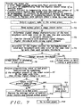
- Fig. 7 A more detailed description of a method to achieve the objectives of this invention is illustrated in Fig. 7.
- First provide, ( 70 ) the means for a color image-sensing array with Bayer pattern RGB, a circuit to sequentially read the digital sensor value of a series of pixels, a memory circuit to temporarily store the read-out values of several pixels before and behind a specific pixel for investigation, an arrangement of circuits to determine a variety of aspects, when comparing values of neighboring pixels on the same row and a circuit to replace said specific pixel's value by a new value.
- a specific pixel as the pixel-under-investigation ( 71 ) and read its sensor value ( 72 ). Then determine the sensor signal change characteristics of the next neighbors with the same color on the same line ( 73 ) and calculate a variable threshold - a smaller threshold in case of moderate signal changes and a higher threshold in case of strong signal changes. Next, determine if the sensor signal change characteristic falls within an anticipated range by determining whether the signal of said pixel-under-investigation exceeds the maximum/minimum of said next neighbors of the same color on the same line by more than said variable threshold ( 74 ) or not. If ( 75 ) it falls within said anticipated range it is most likely a good pixel ( 712 ). If however it exceeds the anticipated threshold, the pixel under investigation may be a bad pixel ( 76 ).
- said pixel under investigation may be a bad pixel
- perform said plausibility check ( 77 ) to find out if it is a true bad pixel. For this purpose, examine, if the neighbor pixels of an other color on the same scan-line, show strong signal changes as well. If neighbor pixels of an other color show strong change ( 78 ) as well, a strong signal change of the pixel under investigation could be anticipated and the pixel is more likely a good pixel ( 711 ). If however the neighbor pixels of an other color show only moderate change, a strong signal change of the pixel under investigation indicates a truly bad pixel ( 79 ). In this case replace the detected bad pixel by an average value of the nearest pixels of the same color before and behind said pixel under investigation ( 710 ).
Landscapes
- Engineering & Computer Science (AREA)
- Multimedia (AREA)
- Signal Processing (AREA)
- Physics & Mathematics (AREA)
- Spectroscopy & Molecular Physics (AREA)
- Transforming Light Signals Into Electric Signals (AREA)
- Color Television Image Signal Generators (AREA)
Priority Applications (2)
| Application Number | Priority Date | Filing Date | Title |
|---|---|---|---|
| EP04392022A EP1594308A1 (de) | 2004-05-07 | 2004-05-07 | Korrektur von defekten RGB Bildpunkten einer einzelnen Zeile eines Bayerfilters |
| US10/859,798 US20050248671A1 (en) | 2004-05-07 | 2004-06-03 | Single line bayer RGB bad pixel correction |
Applications Claiming Priority (1)
| Application Number | Priority Date | Filing Date | Title |
|---|---|---|---|
| EP04392022A EP1594308A1 (de) | 2004-05-07 | 2004-05-07 | Korrektur von defekten RGB Bildpunkten einer einzelnen Zeile eines Bayerfilters |
Publications (1)
| Publication Number | Publication Date |
|---|---|
| EP1594308A1 true EP1594308A1 (de) | 2005-11-09 |
Family
ID=34931978
Family Applications (1)
| Application Number | Title | Priority Date | Filing Date |
|---|---|---|---|
| EP04392022A Withdrawn EP1594308A1 (de) | 2004-05-07 | 2004-05-07 | Korrektur von defekten RGB Bildpunkten einer einzelnen Zeile eines Bayerfilters |
Country Status (2)
| Country | Link |
|---|---|
| US (1) | US20050248671A1 (de) |
| EP (1) | EP1594308A1 (de) |
Cited By (11)
| Publication number | Priority date | Publication date | Assignee | Title |
|---|---|---|---|---|
| WO2007085006A1 (en) * | 2006-01-19 | 2007-07-26 | Qualcomm Incorporated | Method and apparatus for defective pixel detection based on the human visual system |
| WO2007106898A1 (en) * | 2006-03-15 | 2007-09-20 | Qualcomm Incorporated | Processing of sensor values in imaging systems |
| WO2008080155A3 (en) * | 2006-12-22 | 2008-09-12 | Qualcomm Inc | Programmable pattern matching device |
| EP2257044A1 (de) * | 2009-05-29 | 2010-12-01 | Thomson Licensing SA | Verfahren und Vorrichtung zur Verarbeitung eines Rohausgabewerts eines Zielpixels |
| EP2101487A3 (de) * | 2008-03-12 | 2011-07-20 | Victor Company of Japan Ltd. | Bilderzeugungsvorrichtung und darin implementiertes Pixelfehlerkompensationsverfahren |
| US8164660B2 (en) | 2008-10-28 | 2012-04-24 | Omnivision Technologies, Inc. | Single row based defective pixel correction |
| GB2524644A (en) * | 2014-02-27 | 2015-09-30 | Canon Kk | Image processing apparatus and method for controlling the same |
| US9635292B2 (en) | 2014-02-27 | 2017-04-25 | Canon Kabushiki Kaisha | Image processing apparatus and method for controlling image processing apparatus |
| EP1777940B1 (de) * | 2005-10-18 | 2017-12-06 | Ricoh Company, Ltd. | Vorrichtung und Verfahren zur Verminderung von Bildrauschen |
| KR20180031678A (ko) * | 2015-06-26 | 2018-03-28 | 율리스 | 적외선 화상 포착 장치의 기생 화소들의 검출 |
| US12482065B2 (en) | 2022-03-30 | 2025-11-25 | Samsung Electronics Co., Ltd. | Learning based bad pixel correction |
Families Citing this family (53)
| Publication number | Priority date | Publication date | Assignee | Title |
|---|---|---|---|---|
| DE60224035D1 (de) * | 2002-08-23 | 2008-01-24 | St Microelectronics Srl | Verfahren zur Rauschfilterung einer numerischen Bildfolge |
| US8471852B1 (en) | 2003-05-30 | 2013-06-25 | Nvidia Corporation | Method and system for tessellation of subdivision surfaces |
| EP1605403A1 (de) * | 2004-06-08 | 2005-12-14 | STMicroelectronics S.r.l. | Filtrage d'images bruitées |
| TWI256847B (en) * | 2004-08-30 | 2006-06-11 | Via Tech Inc | Method and apparatus for dynamically detecting pixel values |
| TWI293454B (en) * | 2004-09-20 | 2008-02-11 | Processor and related method for adjusting color attributes of a pixel | |
| TWI244330B (en) * | 2004-10-21 | 2005-11-21 | Novatek Microelectronics Corp | Image sensing device with pixel correction function and method for correcting pixel sensing-information in an image sensing device |
| KR100688538B1 (ko) * | 2005-03-22 | 2007-03-02 | 삼성전자주식회사 | 디스플레이 패널에서 내부 메모리 스킴 변경을 통한 배치 면적을 최소화하는 디스플레이 패널 구동 회로 및 이를 이용한 디스플레이 패널 회로 구동 방법 |
| US7683948B2 (en) * | 2005-03-31 | 2010-03-23 | Freescale Semiconductor, Inc. | System and method for bad pixel replacement in image processing |
| JP4388909B2 (ja) * | 2005-04-25 | 2009-12-24 | イーストマン コダック カンパニー | 画素欠陥補正装置 |
| KR100652408B1 (ko) * | 2005-04-27 | 2006-12-01 | 삼성전자주식회사 | 베이어 패턴의 디지털 컬러 영상 신호를 처리하는 방법 및장치 |
| US8571346B2 (en) * | 2005-10-26 | 2013-10-29 | Nvidia Corporation | Methods and devices for defective pixel detection |
| US7885458B1 (en) | 2005-10-27 | 2011-02-08 | Nvidia Corporation | Illuminant estimation using gamut mapping and scene classification |
| US7750956B2 (en) | 2005-11-09 | 2010-07-06 | Nvidia Corporation | Using a graphics processing unit to correct video and audio data |
| US8588542B1 (en) | 2005-12-13 | 2013-11-19 | Nvidia Corporation | Configurable and compact pixel processing apparatus |
| US8737832B1 (en) | 2006-02-10 | 2014-05-27 | Nvidia Corporation | Flicker band automated detection system and method |
| US8630498B2 (en) | 2006-03-02 | 2014-01-14 | Sharp Laboratories Of America, Inc. | Methods and systems for detecting pictorial regions in digital images |
| US7864365B2 (en) * | 2006-06-15 | 2011-01-04 | Sharp Laboratories Of America, Inc. | Methods and systems for segmenting a digital image into regions |
| US8437054B2 (en) * | 2006-06-15 | 2013-05-07 | Sharp Laboratories Of America, Inc. | Methods and systems for identifying regions of substantially uniform color in a digital image |
| US7876959B2 (en) | 2006-09-06 | 2011-01-25 | Sharp Laboratories Of America, Inc. | Methods and systems for identifying text in digital images |
| US8594441B1 (en) | 2006-09-12 | 2013-11-26 | Nvidia Corporation | Compressing image-based data using luminance |
| US8723969B2 (en) | 2007-03-20 | 2014-05-13 | Nvidia Corporation | Compensating for undesirable camera shakes during video capture |
| US8885076B2 (en) * | 2007-03-30 | 2014-11-11 | Hewlett-Packard Development Company, L.P. | Camera sensor defect correction and noise reduction |
| US8564687B2 (en) * | 2007-05-07 | 2013-10-22 | Nvidia Corporation | Efficient determination of an illuminant of a scene |
| JP2008301142A (ja) * | 2007-05-31 | 2008-12-11 | Fujitsu Microelectronics Ltd | 固体撮像素子および画素補正方法 |
| US8698917B2 (en) * | 2007-06-04 | 2014-04-15 | Nvidia Corporation | Reducing computational complexity in determining an illuminant of a scene |
| JP2009017475A (ja) * | 2007-07-09 | 2009-01-22 | Elmo Co Ltd | 欠陥画素検出装置、撮像装置、および、欠陥画素の検出方法 |
| US8724895B2 (en) | 2007-07-23 | 2014-05-13 | Nvidia Corporation | Techniques for reducing color artifacts in digital images |
| US8570634B2 (en) | 2007-10-11 | 2013-10-29 | Nvidia Corporation | Image processing of an incoming light field using a spatial light modulator |
| US9177368B2 (en) | 2007-12-17 | 2015-11-03 | Nvidia Corporation | Image distortion correction |
| US8780128B2 (en) | 2007-12-17 | 2014-07-15 | Nvidia Corporation | Contiguously packed data |
| US8698908B2 (en) | 2008-02-11 | 2014-04-15 | Nvidia Corporation | Efficient method for reducing noise and blur in a composite still image from a rolling shutter camera |
| US9379156B2 (en) | 2008-04-10 | 2016-06-28 | Nvidia Corporation | Per-channel image intensity correction |
| US8373718B2 (en) | 2008-12-10 | 2013-02-12 | Nvidia Corporation | Method and system for color enhancement with color volume adjustment and variable shift along luminance axis |
| US9544516B2 (en) * | 2008-12-26 | 2017-01-10 | Digimarc Corporation | Method and apparatus for sensor characterization |
| US8749662B2 (en) | 2009-04-16 | 2014-06-10 | Nvidia Corporation | System and method for lens shading image correction |
| US8698918B2 (en) | 2009-10-27 | 2014-04-15 | Nvidia Corporation | Automatic white balancing for photography |
| US9798698B2 (en) | 2012-08-13 | 2017-10-24 | Nvidia Corporation | System and method for multi-color dilu preconditioner |
| US9508318B2 (en) | 2012-09-13 | 2016-11-29 | Nvidia Corporation | Dynamic color profile management for electronic devices |
| US9307213B2 (en) | 2012-11-05 | 2016-04-05 | Nvidia Corporation | Robust selection and weighting for gray patch automatic white balancing |
| CN103888690B (zh) * | 2012-12-19 | 2018-08-03 | 韩华泰科株式会社 | 用于检测缺陷像素的设备和方法 |
| JP6089872B2 (ja) * | 2013-03-28 | 2017-03-08 | 富士通株式会社 | 画像補正装置、画像補正方法及び生体認証装置 |
| US9418400B2 (en) | 2013-06-18 | 2016-08-16 | Nvidia Corporation | Method and system for rendering simulated depth-of-field visual effect |
| US9756222B2 (en) | 2013-06-26 | 2017-09-05 | Nvidia Corporation | Method and system for performing white balancing operations on captured images |
| US9826208B2 (en) | 2013-06-26 | 2017-11-21 | Nvidia Corporation | Method and system for generating weights for use in white balancing an image |
| GB2545198A (en) * | 2015-12-08 | 2017-06-14 | Thermoteknix Systems Ltd | Identification of faulty sensing elements in sensing element arrays |
| CN105551003B (zh) * | 2015-12-21 | 2018-09-28 | 核工业北京地质研究院 | 一种图像条带噪声及坏线消除方法 |
| CN107248147B (zh) * | 2017-06-07 | 2020-03-31 | 思特威(上海)电子科技有限公司 | Raw-rgb图像中坏点消除的方法 |
| US11087656B2 (en) | 2019-08-15 | 2021-08-10 | Samsung Display Co., Ltd. | Fully differential front end for sensing |
| US11069282B2 (en) | 2019-08-15 | 2021-07-20 | Samsung Display Co., Ltd. | Correlated double sampling pixel sensing front end |
| US11250780B2 (en) | 2019-08-15 | 2022-02-15 | Samsung Display Co., Ltd. | Estimation of pixel compensation coefficients by adaptation |
| US11081064B1 (en) | 2020-01-13 | 2021-08-03 | Samsung Display Co., Ltd. | Reference signal generation by reusing the driver circuit |
| US11257416B2 (en) | 2020-02-14 | 2022-02-22 | Samsung Display Co., Ltd. | Voltage mode pre-emphasis with floating phase |
| US11719738B2 (en) | 2020-10-15 | 2023-08-08 | Samsung Display Co., Ltd. | Two-domain two-stage sensing front-end circuits and systems |
Citations (4)
| Publication number | Priority date | Publication date | Assignee | Title |
|---|---|---|---|---|
| EP1045578A2 (de) * | 1999-03-15 | 2000-10-18 | Texas Instruments Incorporated | Filterung defekter Bildelemente bei digitalen Bildgebern |
| US20030151682A1 (en) * | 2002-02-08 | 2003-08-14 | Fujitsu Limited | Circuit for correction of white pixel defects and an image sensor using the circuit for correction of white pixel defects |
| WO2004004319A1 (en) * | 2002-07-01 | 2004-01-08 | Koninklijke Philips Electronics N.V. | Device and method of detection of erroneous image sample data of defective image samples |
| EP1401196A1 (de) * | 2002-09-18 | 2004-03-24 | Agilent Technologies, Inc. | Verfahren zum Detektieren und Korrigieren von defekten Bildpunkten in einem digitalen Bildsensor |
Family Cites Families (5)
| Publication number | Priority date | Publication date | Assignee | Title |
|---|---|---|---|---|
| US4535359A (en) * | 1983-01-17 | 1985-08-13 | Eastman Kodak Company | Defect correction in solid state imaging |
| US5047863A (en) * | 1990-05-24 | 1991-09-10 | Polaroid Corporation | Defect correction apparatus for solid state imaging devices including inoperative pixel detection |
| JP3125124B2 (ja) * | 1994-06-06 | 2001-01-15 | 松下電器産業株式会社 | 欠陥画素傷補正回路 |
| JP2000285229A (ja) * | 1999-03-15 | 2000-10-13 | Texas Instr Inc <Ti> | ディジタルイメージャのための不良画素フィルタリング |
| JP3747909B2 (ja) * | 2002-12-24 | 2006-02-22 | ソニー株式会社 | 画素欠陥検出補正装置及び画素欠陥検出補正方法 |
-
2004
- 2004-05-07 EP EP04392022A patent/EP1594308A1/de not_active Withdrawn
- 2004-06-03 US US10/859,798 patent/US20050248671A1/en not_active Abandoned
Patent Citations (4)
| Publication number | Priority date | Publication date | Assignee | Title |
|---|---|---|---|---|
| EP1045578A2 (de) * | 1999-03-15 | 2000-10-18 | Texas Instruments Incorporated | Filterung defekter Bildelemente bei digitalen Bildgebern |
| US20030151682A1 (en) * | 2002-02-08 | 2003-08-14 | Fujitsu Limited | Circuit for correction of white pixel defects and an image sensor using the circuit for correction of white pixel defects |
| WO2004004319A1 (en) * | 2002-07-01 | 2004-01-08 | Koninklijke Philips Electronics N.V. | Device and method of detection of erroneous image sample data of defective image samples |
| EP1401196A1 (de) * | 2002-09-18 | 2004-03-24 | Agilent Technologies, Inc. | Verfahren zum Detektieren und Korrigieren von defekten Bildpunkten in einem digitalen Bildsensor |
Cited By (17)
| Publication number | Priority date | Publication date | Assignee | Title |
|---|---|---|---|---|
| EP1777940B1 (de) * | 2005-10-18 | 2017-12-06 | Ricoh Company, Ltd. | Vorrichtung und Verfahren zur Verminderung von Bildrauschen |
| US7920186B2 (en) | 2006-01-19 | 2011-04-05 | Qualcomm Incorporated | Method and apparatus for defective pixel detection based on the human visual system |
| WO2007085006A1 (en) * | 2006-01-19 | 2007-07-26 | Qualcomm Incorporated | Method and apparatus for defective pixel detection based on the human visual system |
| WO2007106898A1 (en) * | 2006-03-15 | 2007-09-20 | Qualcomm Incorporated | Processing of sensor values in imaging systems |
| US7667747B2 (en) | 2006-03-15 | 2010-02-23 | Qualcomm Incorporated | Processing of sensor values in imaging systems |
| US8077228B2 (en) | 2006-03-15 | 2011-12-13 | Qualcomm Incorporated | Processing of sensor values in imaging systems |
| US7800661B2 (en) | 2006-12-22 | 2010-09-21 | Qualcomm Incorporated | Programmable pattern matching device |
| WO2008080155A3 (en) * | 2006-12-22 | 2008-09-12 | Qualcomm Inc | Programmable pattern matching device |
| EP2101487A3 (de) * | 2008-03-12 | 2011-07-20 | Victor Company of Japan Ltd. | Bilderzeugungsvorrichtung und darin implementiertes Pixelfehlerkompensationsverfahren |
| US8164660B2 (en) | 2008-10-28 | 2012-04-24 | Omnivision Technologies, Inc. | Single row based defective pixel correction |
| EP2257044A1 (de) * | 2009-05-29 | 2010-12-01 | Thomson Licensing SA | Verfahren und Vorrichtung zur Verarbeitung eines Rohausgabewerts eines Zielpixels |
| GB2524644A (en) * | 2014-02-27 | 2015-09-30 | Canon Kk | Image processing apparatus and method for controlling the same |
| GB2524644B (en) * | 2014-02-27 | 2016-10-05 | Canon Kk | Image processing apparatus and method for controlling the same |
| US9635292B2 (en) | 2014-02-27 | 2017-04-25 | Canon Kabushiki Kaisha | Image processing apparatus and method for controlling image processing apparatus |
| US9693000B2 (en) | 2014-02-27 | 2017-06-27 | Canon Kabushiki Kaisha | Image processing apparatus and method for controlling image processing apparatus |
| KR20180031678A (ko) * | 2015-06-26 | 2018-03-28 | 율리스 | 적외선 화상 포착 장치의 기생 화소들의 검출 |
| US12482065B2 (en) | 2022-03-30 | 2025-11-25 | Samsung Electronics Co., Ltd. | Learning based bad pixel correction |
Also Published As
| Publication number | Publication date |
|---|---|
| US20050248671A1 (en) | 2005-11-10 |
Similar Documents
| Publication | Publication Date | Title |
|---|---|---|
| US20050248671A1 (en) | Single line bayer RGB bad pixel correction | |
| US6965395B1 (en) | Methods and systems for detecting defective imaging pixels and pixel values | |
| JP4378746B2 (ja) | 欠陥ピクセルの検出可能なディジタル・イメージ・センサおよび方法 | |
| JP3984936B2 (ja) | 撮像装置および撮像方法 | |
| EP1389771B1 (de) | Digitalbildverfahren und -vorrichtung zum zusammenfügen von Entfernung des Mosaikeffekts und Korrektur von schlechten Pixeln | |
| EP2026563A1 (de) | Vorrichtung und Verfahren zur Erkennung defekter Pixel | |
| US8310577B1 (en) | Method and apparatus for color compensation | |
| US7183532B2 (en) | Detecting a defect in an image scanner | |
| US20050243181A1 (en) | Device and method of detection of erroneous image sample data of defective image samples | |
| CN103404123B (zh) | 成像装置和缺陷像素校正方法 | |
| US8035702B2 (en) | Pixel defect correction device for line crawl | |
| KR101666137B1 (ko) | 이미지 캡쳐 시스템에서 결함 평가방법 및 관련 시스템 | |
| US7911514B2 (en) | Defective pixel correction device | |
| JP5541718B2 (ja) | 撮像装置及びその欠陥画素検出方法 | |
| JP2000285229A (ja) | ディジタルイメージャのための不良画素フィルタリング | |
| US20100066872A1 (en) | Image sensing apparatus and defective pixel detection method | |
| CN101198965A (zh) | 图像传感器中的缺陷像素校正 | |
| KR101012626B1 (ko) | 인간 시각 시스템에 기초한 결함 화소 검출을 위한 방법 및장치 | |
| JP3696069B2 (ja) | 固体撮像素子の欠陥画素検出方法および装置 | |
| JP2003198946A (ja) | 撮像装置及びその欠陥画素処理方法 | |
| JP3767188B2 (ja) | 電子カメラ及び信号補正方法 | |
| JP2002101342A (ja) | 撮像素子の欠陥画素検出方法 | |
| JP3494573B2 (ja) | シート面の検査装置 | |
| Tajbakhsh | Efficient defect pixel cluster detection and correction for Bayer CFA image sequences | |
| JP2004112025A (ja) | 固体撮像素子の欠陥画素補正装置 |
Legal Events
| Date | Code | Title | Description |
|---|---|---|---|
| PUAI | Public reference made under article 153(3) epc to a published international application that has entered the european phase |
Free format text: ORIGINAL CODE: 0009012 |
|
| AK | Designated contracting states |
Kind code of ref document: A1 Designated state(s): AT BE BG CH CY CZ DE DK EE ES FI FR GB GR HU IE IT LI LU MC NL PL PT RO SE SI SK TR |
|
| AX | Request for extension of the european patent |
Extension state: AL HR LT LV MK |
|
| AKX | Designation fees paid | ||
| 17P | Request for examination filed |
Effective date: 20060508 |
|
| RBV | Designated contracting states (corrected) |
Designated state(s): AT BE BG CH CY CZ DE DK EE ES FI FR GB GR HU IE IT LI LU MC NL PL PT RO SE SI SK TR |
|
| REG | Reference to a national code |
Ref country code: DE Ref legal event code: 8566 |
|
| 17Q | First examination report despatched |
Effective date: 20071116 |
|
| STAA | Information on the status of an ep patent application or granted ep patent |
Free format text: STATUS: THE APPLICATION IS DEEMED TO BE WITHDRAWN |
|
| 18D | Application deemed to be withdrawn |
Effective date: 20080327 |