EP1595111B1 - Modulateur de phase numerique pour un dispositif a fibres optiques - Google Patents
Modulateur de phase numerique pour un dispositif a fibres optiques Download PDFInfo
- Publication number
- EP1595111B1 EP1595111B1 EP04712523A EP04712523A EP1595111B1 EP 1595111 B1 EP1595111 B1 EP 1595111B1 EP 04712523 A EP04712523 A EP 04712523A EP 04712523 A EP04712523 A EP 04712523A EP 1595111 B1 EP1595111 B1 EP 1595111B1
- Authority
- EP
- European Patent Office
- Prior art keywords
- electrodes
- modulator
- electrode
- phase
- value
- Prior art date
- Legal status (The legal status is an assumption and is not a legal conclusion. Google has not performed a legal analysis and makes no representation as to the accuracy of the status listed.)
- Expired - Lifetime
Links
- 238000000034 method Methods 0.000 claims description 12
- 230000008054 signal transmission Effects 0.000 claims description 8
- 230000003287 optical effect Effects 0.000 claims description 6
- 239000000758 substrate Substances 0.000 claims description 6
- 230000000694 effects Effects 0.000 claims description 5
- 239000012876 carrier material Substances 0.000 claims 1
- 238000012937 correction Methods 0.000 description 20
- 239000000835 fiber Substances 0.000 description 8
- 238000006243 chemical reaction Methods 0.000 description 6
- 238000004519 manufacturing process Methods 0.000 description 5
- 238000013461 design Methods 0.000 description 4
- 238000010586 diagram Methods 0.000 description 4
- 230000010363 phase shift Effects 0.000 description 4
- 241001136792 Alle Species 0.000 description 2
- 238000013459 approach Methods 0.000 description 2
- 230000008033 biological extinction Effects 0.000 description 2
- 229910013641 LiNbO 3 Inorganic materials 0.000 description 1
- 230000032683 aging Effects 0.000 description 1
- 230000006399 behavior Effects 0.000 description 1
- 238000010276 construction Methods 0.000 description 1
- 230000005684 electric field Effects 0.000 description 1
- 230000006870 function Effects 0.000 description 1
- GQYHUHYESMUTHG-UHFFFAOYSA-N lithium niobate Chemical compound [Li+].[O-][Nb](=O)=O GQYHUHYESMUTHG-UHFFFAOYSA-N 0.000 description 1
- 238000012545 processing Methods 0.000 description 1
- 230000004044 response Effects 0.000 description 1
- 238000000926 separation method Methods 0.000 description 1
- 238000005476 soldering Methods 0.000 description 1
- 238000009827 uniform distribution Methods 0.000 description 1
Images


Classifications
-
- G—PHYSICS
- G01—MEASURING; TESTING
- G01C—MEASURING DISTANCES, LEVELS OR BEARINGS; SURVEYING; NAVIGATION; GYROSCOPIC INSTRUMENTS; PHOTOGRAMMETRY OR VIDEOGRAMMETRY
- G01C19/00—Gyroscopes; Turn-sensitive devices using vibrating masses; Turn-sensitive devices without moving masses; Measuring angular rate using gyroscopic effects
- G01C19/58—Turn-sensitive devices without moving masses
- G01C19/64—Gyrometers using the Sagnac effect, i.e. rotation-induced shifts between counter-rotating electromagnetic beams
- G01C19/72—Gyrometers using the Sagnac effect, i.e. rotation-induced shifts between counter-rotating electromagnetic beams with counter-rotating light beams in a passive ring, e.g. fibre laser gyrometers
- G01C19/726—Phase nulling gyrometers, i.e. compensating the Sagnac phase shift in a closed loop system
-
- G—PHYSICS
- G02—OPTICS
- G02F—OPTICAL DEVICES OR ARRANGEMENTS FOR THE CONTROL OF LIGHT BY MODIFICATION OF THE OPTICAL PROPERTIES OF THE MEDIA OF THE ELEMENTS INVOLVED THEREIN; NON-LINEAR OPTICS; FREQUENCY-CHANGING OF LIGHT; OPTICAL LOGIC ELEMENTS; OPTICAL ANALOGUE/DIGITAL CONVERTERS
- G02F1/00—Devices or arrangements for the control of the intensity, colour, phase, polarisation or direction of light arriving from an independent light source, e.g. switching, gating or modulating; Non-linear optics
- G02F1/01—Devices or arrangements for the control of the intensity, colour, phase, polarisation or direction of light arriving from an independent light source, e.g. switching, gating or modulating; Non-linear optics for the control of the intensity, phase, polarisation or colour
- G02F1/011—Devices or arrangements for the control of the intensity, colour, phase, polarisation or direction of light arriving from an independent light source, e.g. switching, gating or modulating; Non-linear optics for the control of the intensity, phase, polarisation or colour in optical waveguides, not otherwise provided for in this subclass
- G02F1/0115—Devices or arrangements for the control of the intensity, colour, phase, polarisation or direction of light arriving from an independent light source, e.g. switching, gating or modulating; Non-linear optics for the control of the intensity, phase, polarisation or colour in optical waveguides, not otherwise provided for in this subclass in optical fibres
-
- G—PHYSICS
- G02—OPTICS
- G02F—OPTICAL DEVICES OR ARRANGEMENTS FOR THE CONTROL OF LIGHT BY MODIFICATION OF THE OPTICAL PROPERTIES OF THE MEDIA OF THE ELEMENTS INVOLVED THEREIN; NON-LINEAR OPTICS; FREQUENCY-CHANGING OF LIGHT; OPTICAL LOGIC ELEMENTS; OPTICAL ANALOGUE/DIGITAL CONVERTERS
- G02F1/00—Devices or arrangements for the control of the intensity, colour, phase, polarisation or direction of light arriving from an independent light source, e.g. switching, gating or modulating; Non-linear optics
- G02F1/01—Devices or arrangements for the control of the intensity, colour, phase, polarisation or direction of light arriving from an independent light source, e.g. switching, gating or modulating; Non-linear optics for the control of the intensity, phase, polarisation or colour
- G02F1/03—Devices or arrangements for the control of the intensity, colour, phase, polarisation or direction of light arriving from an independent light source, e.g. switching, gating or modulating; Non-linear optics for the control of the intensity, phase, polarisation or colour based on ceramics or electro-optical crystals, e.g. exhibiting Pockels effect or Kerr effect
- G02F1/0305—Constructional arrangements
- G02F1/0316—Electrodes
-
- G—PHYSICS
- G02—OPTICS
- G02F—OPTICAL DEVICES OR ARRANGEMENTS FOR THE CONTROL OF LIGHT BY MODIFICATION OF THE OPTICAL PROPERTIES OF THE MEDIA OF THE ELEMENTS INVOLVED THEREIN; NON-LINEAR OPTICS; FREQUENCY-CHANGING OF LIGHT; OPTICAL LOGIC ELEMENTS; OPTICAL ANALOGUE/DIGITAL CONVERTERS
- G02F2201/00—Constructional arrangements not provided for in groups G02F1/00 - G02F7/00
- G02F2201/12—Constructional arrangements not provided for in groups G02F1/00 - G02F7/00 electrode
- G02F2201/122—Constructional arrangements not provided for in groups G02F1/00 - G02F7/00 electrode having a particular pattern
-
- G—PHYSICS
- G02—OPTICS
- G02F—OPTICAL DEVICES OR ARRANGEMENTS FOR THE CONTROL OF LIGHT BY MODIFICATION OF THE OPTICAL PROPERTIES OF THE MEDIA OF THE ELEMENTS INVOLVED THEREIN; NON-LINEAR OPTICS; FREQUENCY-CHANGING OF LIGHT; OPTICAL LOGIC ELEMENTS; OPTICAL ANALOGUE/DIGITAL CONVERTERS
- G02F2203/00—Function characteristic
- G02F2203/50—Phase-only modulation
Definitions
- the invention relates to a method for increasing the resolution of a digital phase modulator for a fiber optic signal transmission or measuring device, which is equipped with a predetermined total number of parallel and arranged on both sides to a light guide path in or on an optical substrate electrodes of different lengths, wherein the electrodes to both Preferably, the same control potential is applied to the sides of the light-guiding path in such a way that a large number of phase values are set by changing the selection of electrode combinations within a predetermined value range.
- the electrodes of the phase modulator are preferably applied to the control with the same potentials, which, depending on the position of the electrodes to the light guide path, cause a positive or negative shift of the light phase at the output of the modulator.
- the electrodes are also referred to as "positive” and “negative” electrodes for short.
- the invention also relates to a digital phase modulator with increased resolution according to the preamble of patent claim 8.
- the number n 0 of the electrodes of the fine modulator is even, where n 0 ⁇ n.
- the fine modulator can also have an asymmetrical number of electrodes, ie the number of electrodes of the fine modulator is then unevenly distributed on the two sides of the light guide path, for which examples are given below. It is important, however, that on the side of the longest electrode of the coarse modulator at least one electrode of the fine modulator is placed, as in the embodiments of the following explained Fig. 1 or 5 is the case.
- a phase modulator according to the invention is generally realized as a unit within or on a multifunctional integrated optical chip (MIOC), on or in the substrate of which - for example, lithium niobate (LiNbO 3 ) - polarization-maintaining light guide sections can be realized.
- MIOC multifunctional integrated optical chip
- a polarizer in addition to a beam splitter.
- the phase modulator itself ie its different lengths of positive and negative electrodes, affect the phases of the two opposing light paths after a branch. Since a MIOC with an integrated digital phase modulator is known in principle, details that are irrelevant to the invention will not be discussed further.
- the invention takes a different approach: proposing a combined modulator configuration without the need for a correction table and without lengthening the overall design, combining binary and non-binary electrode groups.
- the invention uses as a core idea the idea that to achieve a finer resolution than given by the shortest electrode, value differences between positive and negative electrodes overlapping in their area of effect are used.
- the overall resolution of the phase modulator is significantly better than the ratio of the total length to the length of the shortest electrode.
- Fig. 1 12 illustrates, in a schematic enlarged representation, a first exemplary embodiment of a digital phase modulator with increased resolution according to the invention.
- This phase modulator comprises a total of twelve electrodes of different length and weight, designated E0, E1, ... E10, E11.
- E0, E1, ... E10, E11 the total of twelve electrodes of different length and weight.
- the electrodes E0, E1 and E4 to E10 arranged to the left of an optical waveguide L represent or occupy value positions b 0 , b 1 and b 4 to b 10
- the electrodes E2, E3 and E11 arranged on the right side of the waveguide L have value positions b 2 occupy b 3 and b 11 .
- the values or numbers can be 1 . 2 . U . U . U . U . 7 . 8th . 9 . 10 . U . U . U . U . 17 with both signs as well as the zero represent.
- Table 1 The resulting electrode separation and weighting of the electrodes E0 to E11 at the positions b 0 to b 11 is shown in Table 1 below as an example of a constructed electrode length sequence with an output dynamic range of> 1: 2 11.5 .
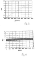
- FIG. 2 illustrated example of the output characteristic for a digital phase modulator Fig. 1 illustrates a range of values from -1650 to +1650 with correspondingly assigned addresses from a drive logic.
- the phase response is obviously perfectly linear.
- the plot of the Fig. 4 shows for the electrode configuration Fig. 1 the range of deviations from linear behavior, ie the remaining deviations from an ideal characteristic.
- the heretofore shown for a hybrid electrode structure according to The invention relates to a first proven example of a possible determination and design of the electrode lengths. Decisive for this are the prerequisites and conditions described above for the overall modulator and the requirement that within the address space used (eg 11.7 bits) no gaps occur in the number combination.
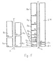
- illustrates the Fig. 5 , wherein the corresponding references to the electrodes E0 to E11 as in Fig. 1 and the corresponding electrode values are again given as b 0 to b 11 .
- Table 2 below illustrates the best possible value or length combination at the moment. Table 2 position value b 0 7:00 b 1 -8.00 b 2 -10.00 b 3 12:00 b 4 16:00 b 5 32.00 b 6 64.00 b 7 128.00 b 8 256.00 b 9 512.00 b 10 1024.00 b 11 -2033.00
- the linear output value range with step size 1: ⁇ 2029 is achieved with a ratio of the longest to the shortest electrode of 290: 1.
- the Fig. 5 thus illustrates a more general electrode structure in which the in Fig. 5 again zoomed out left fine modulator is not symmetrical.
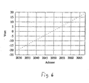
- the Fig. 6 shows a section of the output characteristic for the optimized electrode values according to Table 2. Different than the detail view of the Fig. 3 one obtains a plateau-free characteristic for this case, if the Address range of the converter is limited to the number of available output states. If, on the other hand, the entire address range - in this case 12 bits - is to be exploited for control purposes, the output characteristic curve is created in some places - similar to Fig. 3 illustrates - plateaus because z. For example, with the electrode configuration of Table 2, only 2029 instead of 2048 starting states per sign are contiguously available. The number of possible plateaus can be estimated from the difference (4096 - "Number of output states"). Which of the two options is to be used depends on the respective requirements.
- Table 3 An example of a minimum configuration of the fine modulator, in which only one electrode is located on the side of the longest electrode (MSB) of the coarse modulator, is shown in Table 3 below.
- Table 4 illustrates an example of an asymmetric configuration of the fine modulator. There is one electrode on the "negative” side and three electrodes of the fine modulator on the "positive” side. Table 4 position value fine modulator b 0 7:00 F b 1 11:00 F b 2 13:00 F b 3 15:00 b 4 -16.00 F b 5 30.00 b 6 60.00 b 7 120.00 b 8 240.00 b 9 480.00 b 10 960.00 b 11 -1920.00
- Table 5 gives an example of an electrode configuration having a more reduced aspect ratio and an odd number no of electrodes of the fine modulator.
- the area to be covered with this electrode configuration is 3744 values, each with basic step size.
- the ratio "resolution to overall length” is about 1: 137.
- the indication “F” in turn indicates which electrodes belong to the fine modulator.
- Table 5 is of particular interest since it provides the basis for expanding the phase modulator to e.g. B. represents 13 bits, which then with a length ratio of 272: 1 (this corresponds to the configuration in Table 2), a resolution of> 12.8 bits (> 7450 values) allows.
- phase modulator Insofar as binary signal processing is provided within the control electronics for a phase modulator according to the invention, which will generally be the case, it is possible to use a non-binary phase modulator according to the invention with the aid of a correction table which converts the calculated digital values into non-binary values.
- This correction table can be designed to be programmable in memory and, in addition to the conversion from binary to non-binary values, can also be production-related or operational Correct errors in the phase modulator.
- the Fig. 7 illustrates the basic circuitry.
- a control device (controller) 30 supplies the binary values corresponding to a specific phase value to a conversion or correction table 31 which controls a subsequent switch 32, via which the individual electrodes E0 to E11 of the phase modulator 33 are driven with a signal combination corresponding to the non-binary value become.
- the modified embodiment of the conversion or correction circuit according to Fig. 8 makes it possible to supply an external signal to the correction table, for example a temperature signal or a signal that takes account of aging-related changes as a post-correction.
- a plurality of, for example, four correction tables KT1 to KT4 are provided, which can be integrated in one ASIC and also make it possible in each case to connect an optimized correction table as a function of an external signal.
Landscapes
- Physics & Mathematics (AREA)
- Engineering & Computer Science (AREA)
- Nonlinear Science (AREA)
- General Physics & Mathematics (AREA)
- Optics & Photonics (AREA)
- Power Engineering (AREA)
- Crystallography & Structural Chemistry (AREA)
- Chemical & Material Sciences (AREA)
- Ceramic Engineering (AREA)
- Electromagnetism (AREA)
- Radar, Positioning & Navigation (AREA)
- Remote Sensing (AREA)
- Optical Modulation, Optical Deflection, Nonlinear Optics, Optical Demodulation, Optical Logic Elements (AREA)
Claims (18)
- Procédé pour augmenter la résolution d'un modulateur de phase numérique pour un dispositif de transmission de signaux ou de mesure à fibres optiques équipé d'un nombre total prédéfini m d'électrodes positives et négatives de différentes longueurs qui sont disposées parallèlement et des deux côtés d'une trajectoire de lumière dans ou sur un substrat optique et qui sont aptes à être sollicitées par des potentiels de commande de préférence égaux qui, suivant la position des électrodes par rapport à la trajectoire de lumière, provoquent un déplacement positif ou négatif de la phase de lumière à la sortie du modulateur, étant précisé que grâce à un choix de commande et à des combinaisons alternés d'électrodes à action positive et négative, un grand nombre de valeurs de phase est réglé à l'intérieur d'une plage de valeurs prédéfinie,
caractérisé en ce que- le nombre total m d'électrodes est divisé en deux groupes, étant précisé-- qu'à partir d'un premier groupe de n électrodes est formé un modulateur grossier avec des électrodes à pondération binaire et plus significatives par leur contribution au déphasage lumineux, et à rapport de longueurs bn+1:bn=2,-- qu'un modulateur fin est formé à partir d'un second groupe de n0 électrodes à pondération non binaire et moins significatives par leur contribution au déphasage lumineux, au moins une électrode de modulateur fin étant placée du côté de l'électrode la plus longue (E11) du modulateur grossier, et- les longueurs et, ainsi, les pondérations sur le déphasage lumineux des électrodes disposées sur des côtés différents du modulateur fin sont choisies pour être plus grandes que la résolution (pas de base) du modulateur total, d'une part, et les pas de modulation de phase les plus petits sont produits grâce à la commande simultanée d'électrodes positives et négatives du modulateur fin ou du modulateur fin et du modulateur grossier, d'autre part. - Procédé selon la revendication 1, caractérisé en ce que la valeur (|1|) associée à la plage de valeurs de départ du déphasage lumineux comme pas le plus petit (pas de base) de la plage de valeurs est générée grâce à la commande simultanée d'électrodes opposées, sur la trajectoire de lumière (L) du second groupe de n0 électrodes du modulateur fin.
- Procédé selon la revendication 1, caractérisé en ce qu'on choisit comme nombre d'électrodes du modulateur grossier n=8, la plus longue de ce premier groupe d'électrodes (position b11) étant disposée d'un côté de la trajectoire de lumière tandis que toutes les autres (positions b4 à b10) sont disposées de l'autre côté de la trajectoire de lumière.
- Procédé selon la revendication 3, caractérisé en ce qu'on choisit comme nombre d'électrodes du modulateur fin n0=4, la plus courte (position b0) et la plus longue (position b3) de ce second groupe d'électrodes étant disposées d'un côté du modulateur grossier tandis que les deux électrodes moyennes (positions b1, b2) de ce second groupe d'électrodes sont disposées de l'autre côté du modulateur grossier.
- Procédé selon la revendication 3, caractérisé en ce qu'on choisit comme nombre d'électrodes du modulateur fin n0=4, la plus courte (position b0) et la plus longue (position b3) de ce second groupe d'électrodes étant disposées du côté des autres électrodes (positions b4 à b10) du modulateur grossier tandis que les deux électrodes moyennes (positions b1, b2) de ce second groupe d'électrodes sont disposées du côté de la plus longue électrode (E11) du modulateur grossier.
- Procédé selon la revendication 4, caractérisé en ce que les valeurs suivantes de la plage de valeurs sont associées au second groupe d'électrodes du modulateur fin, grâce à une longueur et à un positionnement correspondants :valeur d'électrode la plus courte (position b0)=7,valeur d'électrode la plus haute (position b3)=10,la plus petite des valeurs d'électrodes moyennes (position b1)=-8la plus grande des valeurs d'électrodes moyennes (position b2)=-9et en ce que les valeurs suivantes de la plage de valeurs sont associées au premier groupe d'électrodes (E4 à E10) du modulateur grossier grâce à une longueur et à un positionnement correspondants :valeur de base binaire de l'électrode la plus courte (position b4) bn=13,valeurs des six électrodes suivantes (positions b5 à b10) bn+1:bn=2 etvaleur de l'électrode la plus longue (E11) (position b11)=-1652.
- Procédé selon la revendication 5, caractérisé en ce que les valeurs suivantes de la plage de valeurs sont associées au second groupe d'électrodes du modulateur fin, grâce à une longueur et à un positionnement correspondants :valeur d'électrode la plus courte (position b0)=7,valeur d'électrode la plus haute (position b3)=12,la plus petite des valeurs d'électrodes moyennes (position b1)=-8la plus grande des valeurs d'électrodes moyennes (position b2)=-10et en ce que les valeurs suivantes de la plage de valeurs sont associées au premier groupe d'électrodes (E4 à E10) du modulateur grossier grâce à une longueur et à un positionnement correspondants :valeur de base binaire de l'électrode la plus courte (position b4) bn=16,valeurs des six électrodes suivantes (positions b5 à b10) bn+1:bn=2 etvaleur de l'électrode la plus longue (E11) (position b11)=-2033.
- Modulateur de phase numérique pour un dispositif de transmission de signaux ou de mesure à fibres optiques qui comporte un nombre total m d'électrodes positives et négatives de différentes longueurs qui sont disposées parallèlement et des deux côtés d'une trajectoire de lumière (L) dans ou sur un substrat optique, les électrodes prévues des deux côtés de la trajectoire de lumière étant aptes à être sollicitées par des potentiels de commande de préférence égaux, provoqués par des intensités de champ opposées, de telle sorte que grâce à des combinaisons alternées d'électrodes positives et négatives un grand nombre de valeurs de phase peut être réglé à l'intérieur d'une plage de valeurs prédéfinie,
caractérisé par- un premier groupe d'électrodes (E4 à E11) qui forme un modulateur grossier avec n électrodes à pondération binaire et plus significatives, avec un rapport de longueurs bn+1:bn d'environ 2, avec n<m ; m=nombre total de toutes les électrodes, étant précisé toutefois que la longueur de l'électrode la plus longue (E11) correspond à la somme des longueurs de toutes les autres électrodes (E0 à E10) du modulateur total avec une valeur de pondération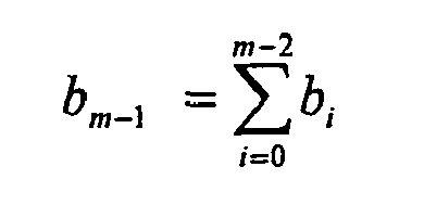 - un second groupe de n0 électrodes à pondération non binaire et moins significatives par leur contribution au déphasage lumineux, qui forme un modulateur fin, avec n+n0=m ; no<n ;- une longueur et une disposition relatives du second groupe de n0 électrodes le long de la trajectoire de lumière (L) qui sont telles que d'une part il n'y a une extinction des valeurs de phase avec aucune combinaison d'électrodes possibles, et que d'autre part le rapport de la plus petite sur la plus grande longueur d'électrode est aussi grand que possible pour une résolution d'environ 1:2-m définie par le nombre total m d'électrodes.
 - Modulateur de phase selon la revendication 8, caractérisé en ce que la plus longue (E11) du premier groupe de n électrodes du modulateur grossier est disposée d'un côté de la trajectoire de lumière (L), tandis que toutes les autres de ce groupe sont disposées de l'autre côté.
- Modulateur de phase selon la revendication 8, caractérisé en ce que les longueurs des électrodes sont choisies de telle sorte que la formation d'une somme ou d'une différence de longueurs d'électrodes donne une plage de valeurs de départ prédéfinie à courbe caractéristique linéaire pour la phase d'un signal sur la trajectoire de lumière, dont la résolution est supérieure au rapport de la plus petite longueur d'électrode sur la longueur totale du modulateur de phase sur le matériau de support.
- Modulateur de phase selon la revendication 9, caractérisé en ce que le plus petit pas de la plage de valeurs de départ de la phase est défini par la plus petite différence de longueur entre les électrodes positives, d'un côté de la trajectoire de lumière, et les électrodes négatives, de l'autre côté de celle-ci.
- Modulateur de phase selon la revendication 8, caractérisé en ce qu'au moins deux électrodes (E1, E2) du modulateur fin qui sont disposées sur des côtés opposés, le long de la trajectoire de lumière, se recouvrent partiellement dans leur zone d'action sur une onde lumineuse qui suit ladite trajectoire de lumière, tandis qu'au moins deux autres électrodes (E0, E3) du modulateur fin qui sont disposées à la suite des premières (E1, E2) sont décalées l'une par rapport à l'autre pour leur zone d'action sur l'onde lumineuse, la plus petite résolution (pas de base) étant définie par la différence de longueur des électrodes qui se recouvrent.
- Modulateur de phase selon la revendication 8, caractérisé en ce que le rapport de la plus petite sur la plus grande longueur d'électrode, pour une longueur prédéfinie de la plus grande électrode du modulateur de phase, est d'environ 1:2-9.
- Modulateur de phase selon la revendication 13, caractérisé en ce que le nombre d'électrodes du modulateur grossier est n=8 et le nombre d'électrodes du modulateur fin est n0=4, et le choix des longueurs des électrodes (E0 à E11) au niveau des positions b0 à b11 est fait de manière à donner une résolution >11 bits.
- Modulateur de phase selon la revendication 13, caractérisé en ce que les longueurs relatives des quatre électrodes du modulateur fin (E0 à E3) sont choisies pour que les valeurs b1=-8, b2=-9 soient fixées au niveau de positions b0 à b3 associées à ces électrodes, du côté de la plus longue électrode (E11) du modulateur grossier avec la position b11, et les valeurs b0=7 et b3=10 sur le côté opposé de la trajectoire de lumière.
- Modulateur de phase selon la revendication 14, caractérisé en ce que les longueurs relatives des électrodes du modulateur grossier sont choisies pour que la pondération de ses électrodes à pondération binaire (E4 à E10) sur le déphasage lumineux commence avec la valeur b4=13 et finisse avec la valeur b10=832, et en ce que la valeur b11=-1652 est attribuée à la plus longue électrode (E11), et en ce que la résolution maximale est de 11,7 bits.
- Modulateur de phase selon la revendication 14, caractérisé en ce que les longueurs relatives des quatre électrodes du modulateur fin (E0 à E3) sont choisies pour que les valeurs b1=-8, b2=-10 soient fixées au niveau de positions b0 à b3 associées à ces électrodes, du côté de la plus longue électrode (E11) du modulateur grossier avec la position b11, et les valeurs b0=7 et b3=12 sur le côté opposé de la trajectoire de lumière.
- Modulateur de phase selon la revendication 17, caractérisé en ce que les longueurs relatives des électrodes du modulateur grossier sont choisies pour que la pondération de ses électrodes à pondération binaire (E4 à E10) sur le déphasage lumineux commence avec la valeur b4=16 et finisse avec la valeur b10=1024, et en ce que la valeur b11=-2033 est attribuée à la plus longue électrode (E11), et en ce que la résolution maximale est de 11,986 bits.
Applications Claiming Priority (3)
| Application Number | Priority Date | Filing Date | Title |
|---|---|---|---|
| DE10307525A DE10307525B4 (de) | 2003-02-21 | 2003-02-21 | Verfahren und Einrichtung zur Erhöhung der Auflösung eines digitalen Phasenmodulators für eine faseroptische Signalübertragungs- oder Messeinrichtung |
| DE10307525 | 2003-02-21 | ||
| PCT/EP2004/001641 WO2004074775A1 (fr) | 2003-02-21 | 2004-02-19 | Modulateur de phase numerique pour un dispositif a fibres optiques |
Publications (2)
| Publication Number | Publication Date |
|---|---|
| EP1595111A1 EP1595111A1 (fr) | 2005-11-16 |
| EP1595111B1 true EP1595111B1 (fr) | 2009-11-11 |
Family
ID=32841789
Family Applications (1)
| Application Number | Title | Priority Date | Filing Date |
|---|---|---|---|
| EP04712523A Expired - Lifetime EP1595111B1 (fr) | 2003-02-21 | 2004-02-19 | Modulateur de phase numerique pour un dispositif a fibres optiques |
Country Status (6)
| Country | Link |
|---|---|
| US (1) | US7469075B2 (fr) |
| EP (1) | EP1595111B1 (fr) |
| CN (1) | CN1751223B (fr) |
| DE (2) | DE10307525B4 (fr) |
| PL (1) | PL378411A1 (fr) |
| WO (1) | WO2004074775A1 (fr) |
Families Citing this family (15)
| Publication number | Priority date | Publication date | Assignee | Title |
|---|---|---|---|---|
| DE102010048488B4 (de) | 2010-10-14 | 2013-01-10 | Northrop Grumman Litef Gmbh | Digitaler Modulator |
| DE102010064440B4 (de) | 2010-10-14 | 2017-11-30 | Northrop Grumman Litef Gmbh | Digitaler integriert-optischer Modulator |
| US9918053B2 (en) * | 2014-05-14 | 2018-03-13 | Jasper Display Corp. | System and method for pulse-width modulating a phase-only spatial light modulator |
| US11030942B2 (en) | 2017-10-13 | 2021-06-08 | Jasper Display Corporation | Backplane adaptable to drive emissive pixel arrays of differing pitches |
| DE112019000242T5 (de) * | 2018-01-31 | 2020-09-03 | Robert Bosch Gmbh | Segmentierter digital-optischer Phasenschieberwandler |
| US10951875B2 (en) | 2018-07-03 | 2021-03-16 | Raxium, Inc. | Display processing circuitry |
| US11710445B2 (en) | 2019-01-24 | 2023-07-25 | Google Llc | Backplane configurations and operations |
| US11637219B2 (en) | 2019-04-12 | 2023-04-25 | Google Llc | Monolithic integration of different light emitting structures on a same substrate |
| US11238782B2 (en) | 2019-06-28 | 2022-02-01 | Jasper Display Corp. | Backplane for an array of emissive elements |
| US11626062B2 (en) | 2020-02-18 | 2023-04-11 | Google Llc | System and method for modulating an array of emissive elements |
| JP7581367B2 (ja) | 2020-04-06 | 2024-11-12 | グーグル エルエルシー | バックプレーン及びディスプレイアセンブリ |
| US12573349B2 (en) | 2020-06-29 | 2026-03-10 | Google Llc | Efficient image data delivery for an array of pixel memory cells |
| US11538431B2 (en) | 2020-06-29 | 2022-12-27 | Google Llc | Larger backplane suitable for high speed applications |
| CN116601547A (zh) | 2020-12-21 | 2023-08-15 | 谷歌有限责任公司 | 用于自由观看3d显示器的高密度像素阵列 |
| EP4371104A4 (fr) | 2021-07-14 | 2025-06-11 | Google LLC | Fond de panier et procédé de modulation de largeur d'impulsion |
Family Cites Families (11)
| Publication number | Priority date | Publication date | Assignee | Title |
|---|---|---|---|---|
| FR2457505A1 (fr) * | 1979-05-23 | 1980-12-19 | Thomson Csf | Modulateur d'intensite lumineuse a commande numerique en optique integree et convertisseur numerique analogique comprenant un tel modulateur |
| GB8531816D0 (en) * | 1985-12-24 | 1986-02-05 | British Aerospace | Phase shifters |
| JPH06103187B2 (ja) * | 1989-05-12 | 1994-12-14 | 日本航空電子工業株式会社 | 光干渉角速度計 |
| US5137359A (en) * | 1991-03-18 | 1992-08-11 | Litton Systems, Inc. | Digital phase modulator for fiber optic sagnac interferometer |
| US5237629A (en) * | 1992-03-19 | 1993-08-17 | The United States Of America As Represented By The United States Department Of Energy | Digitally controlled distributed phase shifter |
| DE19629260C1 (de) * | 1996-07-19 | 1998-02-26 | Litef Gmbh | Elektrooptischer Phasenmodulator mit richtungsunabhängiger Impulsantwort, Anordnung von elektrooptischen Phasenmodulatoren und Verwendung eines elektrooptischen Phasenmodulators |
| DE19753427C1 (de) * | 1997-12-02 | 1999-02-04 | Litef Gmbh | Verfahren und Einrichtung zur Erhöhung der Genauigkeit eines digitalen Phasenmodulators für eine faseroptische Signalübertragungs- oder Meßeinrichtung |
| CN2446688Y (zh) * | 2000-08-25 | 2001-09-05 | 深圳市众量激光器高技术有限公司 | 半导体激光器及激光列阵管芯下电极键合机 |
| DE10112835B4 (de) * | 2001-03-16 | 2006-05-11 | Litef Gmbh | Verfahren und Einrichtung zur Strommessung mittels eines faseroptischen In-Line-Sagnac-Interferometers und dafür geeigneter Phasenmodulator |
| DE10245540B3 (de) * | 2002-09-30 | 2004-09-16 | Litef Gmbh | Verfahren zur Regelung der Arbeitsfrequenz eines faseroptischen Gyroskops |
| DE10307526B4 (de) * | 2003-02-21 | 2005-07-28 | Litef Gmbh | Digitaler Phasenmodulator hoher Auflösung für eine faseroptische Signalübertragungs- oder Messeinrichtung |
-
2003
- 2003-02-21 DE DE10307525A patent/DE10307525B4/de not_active Expired - Fee Related
-
2004
- 2004-02-19 WO PCT/EP2004/001641 patent/WO2004074775A1/fr not_active Ceased
- 2004-02-19 EP EP04712523A patent/EP1595111B1/fr not_active Expired - Lifetime
- 2004-02-19 PL PL378411A patent/PL378411A1/pl not_active IP Right Cessation
- 2004-02-19 US US10/546,414 patent/US7469075B2/en not_active Expired - Lifetime
- 2004-02-19 CN CN200480004656.5A patent/CN1751223B/zh not_active Expired - Lifetime
- 2004-02-19 DE DE502004010349T patent/DE502004010349D1/de not_active Expired - Lifetime
Also Published As
| Publication number | Publication date |
|---|---|
| US20060147146A1 (en) | 2006-07-06 |
| WO2004074775A1 (fr) | 2004-09-02 |
| DE502004010349D1 (de) | 2009-12-24 |
| DE10307525B4 (de) | 2006-03-16 |
| EP1595111A1 (fr) | 2005-11-16 |
| CN1751223B (zh) | 2012-07-25 |
| CN1751223A (zh) | 2006-03-22 |
| PL378411A1 (pl) | 2006-04-03 |
| US7469075B2 (en) | 2008-12-23 |
| DE10307525A1 (de) | 2004-09-09 |
Similar Documents
| Publication | Publication Date | Title |
|---|---|---|
| EP1595111B1 (fr) | Modulateur de phase numerique pour un dispositif a fibres optiques | |
| DE3851927T2 (de) | Flüssigkristall-Anzeigegerät. | |
| DE69115103T2 (de) | Wiedergabeanordnung. | |
| DE2607042C3 (de) | Spannungsauswahlschaltung | |
| DE10224737B4 (de) | Datentreiber-Einrichtung und ein Verfahren für eine Flüssigkristall-Anzeige | |
| DE69030595T2 (de) | Anzeigegerät mit Eingabefunktion | |
| DE19840930B4 (de) | Digital/Analog-Wandler und Treiberschaltkreis für eine Flüssigkristallanzeige | |
| DE102014203925B4 (de) | Elektro-optischer Modulator und Verfahren zum Herstellen eines elektro-optischen Modulators | |
| DE19958049B4 (de) | Transkonduktor und Strommodus D/A-Wandler | |
| DE4003843A1 (de) | Ferroelektrische fluessigkeitskristallanzeige | |
| DE2727010C3 (de) | Verfahren zum Betreiben einer elektrooptischen Anzeigevorrichtung | |
| WO2001009954A1 (fr) | Film actif pour cartes a puce avec affichage | |
| DE2819286B2 (de) | Schaltungsanordnung zur Verbesserung der Anzeigenqualität bei der Darstellung von Zeichen auf Bildschirmen von nach dem Rasterprinzip arbeitenden Sichtgeräten | |
| DE2702034A1 (de) | Anzeigevorrichtung aus aneinander angrenzenden anzeigeelementen, verfahren zur herstellung dieser anzeigevorrichtung sowie verwendung der anzeigevorrichtung in instrumententafeln | |
| DE2832999A1 (de) | Elektrochrome anzeigeeinrichtung | |
| DE3018452A1 (de) | Faksimile-schreibeinrichtung | |
| DE69430895T2 (de) | Anzeigevorrichtung mit Flüssigkristallen | |
| EP1595179B1 (fr) | Modulateur de phase haute resolution pour un dispositif a fibres optiques de transmission de signaux et de mesure | |
| EP0011234A1 (fr) | Dispositif d'affichage électrooptique du type passif, procédé pour commander un tel dispositif d'affichage et son application | |
| EP1036302B1 (fr) | Modulateur de phase numerique | |
| DE2623429C2 (de) | Multiplex-Ansteuerverfahren für eine Flüssigkristall-Anzeige | |
| DE3743498A1 (de) | Fluoreszenz-anzeigeeinrichtung | |
| EP2628045B1 (fr) | Modulateur électro-optique numérique du type à guide d'ondes | |
| DE69216785T2 (de) | Steuerschaltung für eine Anzeigeeinheit mit digitaler Sourcesteuerung zur Erzeugung von Mehrfachpegelsteuerspannungen aus einer einzelnen externen Energiequelle | |
| DE2844059A1 (de) | Integrierte sichtanzeigeeinrichtung |
Legal Events
| Date | Code | Title | Description |
|---|---|---|---|
| PUAI | Public reference made under article 153(3) epc to a published international application that has entered the european phase |
Free format text: ORIGINAL CODE: 0009012 |
|
| 17P | Request for examination filed |
Effective date: 20050812 |
|
| AK | Designated contracting states |
Kind code of ref document: A1 Designated state(s): AT BE BG CH CY CZ DE DK EE ES FI FR GB GR HU IE IT LI LU MC NL PT RO SE SI SK TR |
|
| AX | Request for extension of the european patent |
Extension state: AL LT LV MK |
|
| DAX | Request for extension of the european patent (deleted) | ||
| RBV | Designated contracting states (corrected) |
Designated state(s): CZ DE FR GB |
|
| RIN1 | Information on inventor provided before grant (corrected) |
Inventor name: SPAHLINGER, GUENTER Inventor name: NEWZELLA, ALFONS Inventor name: VOIGT, SVEN |
|
| RAP1 | Party data changed (applicant data changed or rights of an application transferred) |
Owner name: NORTHROP GRUMMAN LITEF GMBH |
|
| GRAP | Despatch of communication of intention to grant a patent |
Free format text: ORIGINAL CODE: EPIDOSNIGR1 |
|
| GRAS | Grant fee paid |
Free format text: ORIGINAL CODE: EPIDOSNIGR3 |
|
| GRAA | (expected) grant |
Free format text: ORIGINAL CODE: 0009210 |
|
| AK | Designated contracting states |
Kind code of ref document: B1 Designated state(s): CZ DE FR GB |
|
| REG | Reference to a national code |
Ref country code: GB Ref legal event code: FG4D Free format text: NOT ENGLISH |
|
| REF | Corresponds to: |
Ref document number: 502004010349 Country of ref document: DE Date of ref document: 20091224 Kind code of ref document: P |
|
| PG25 | Lapsed in a contracting state [announced via postgrant information from national office to epo] |
Ref country code: CZ Free format text: LAPSE BECAUSE OF FAILURE TO SUBMIT A TRANSLATION OF THE DESCRIPTION OR TO PAY THE FEE WITHIN THE PRESCRIBED TIME-LIMIT Effective date: 20091111 |
|
| PLBE | No opposition filed within time limit |
Free format text: ORIGINAL CODE: 0009261 |
|
| STAA | Information on the status of an ep patent application or granted ep patent |
Free format text: STATUS: NO OPPOSITION FILED WITHIN TIME LIMIT |
|
| 26N | No opposition filed |
Effective date: 20100812 |
|
| REG | Reference to a national code |
Ref country code: FR Ref legal event code: PLFP Year of fee payment: 13 |
|
| REG | Reference to a national code |
Ref country code: FR Ref legal event code: PLFP Year of fee payment: 14 |
|
| REG | Reference to a national code |
Ref country code: FR Ref legal event code: PLFP Year of fee payment: 15 |
|
| PGFP | Annual fee paid to national office [announced via postgrant information from national office to epo] |
Ref country code: FR Payment date: 20230220 Year of fee payment: 20 |
|
| PGFP | Annual fee paid to national office [announced via postgrant information from national office to epo] |
Ref country code: GB Payment date: 20230221 Year of fee payment: 20 Ref country code: DE Payment date: 20230223 Year of fee payment: 20 |
|
| REG | Reference to a national code |
Ref country code: DE Ref legal event code: R071 Ref document number: 502004010349 Country of ref document: DE |
|
| REG | Reference to a national code |
Ref country code: GB Ref legal event code: PE20 Expiry date: 20240218 |
|
| PG25 | Lapsed in a contracting state [announced via postgrant information from national office to epo] |
Ref country code: GB Free format text: LAPSE BECAUSE OF EXPIRATION OF PROTECTION Effective date: 20240218 |