EP1596233A1 - Optisches modul - Google Patents
Optisches modul Download PDFInfo
- Publication number
- EP1596233A1 EP1596233A1 EP04712756A EP04712756A EP1596233A1 EP 1596233 A1 EP1596233 A1 EP 1596233A1 EP 04712756 A EP04712756 A EP 04712756A EP 04712756 A EP04712756 A EP 04712756A EP 1596233 A1 EP1596233 A1 EP 1596233A1
- Authority
- EP
- European Patent Office
- Prior art keywords
- optical
- mount
- sub
- fiber
- optical module
- Prior art date
- Legal status (The legal status is an assumption and is not a legal conclusion. Google has not performed a legal analysis and makes no representation as to the accuracy of the status listed.)
- Withdrawn
Links
Images


Classifications
-
- G—PHYSICS
- G02—OPTICS
- G02B—OPTICAL ELEMENTS, SYSTEMS OR APPARATUS
- G02B6/00—Light guides; Structural details of arrangements comprising light guides and other optical elements, e.g. couplings
- G02B6/24—Coupling light guides
- G02B6/42—Coupling light guides with opto-electronic elements
- G02B6/4201—Packages, e.g. shape, construction, internal or external details
- G02B6/4219—Mechanical fixtures for holding or positioning the elements relative to each other in the couplings; Alignment methods for the elements, e.g. measuring or observing methods especially used therefor
- G02B6/4228—Passive alignment, i.e. without a detection of the degree of coupling or the position of the elements
- G02B6/423—Passive alignment, i.e. without a detection of the degree of coupling or the position of the elements using guiding surfaces for the alignment
-
- G—PHYSICS
- G02—OPTICS
- G02B—OPTICAL ELEMENTS, SYSTEMS OR APPARATUS
- G02B6/00—Light guides; Structural details of arrangements comprising light guides and other optical elements, e.g. couplings
- G02B6/24—Coupling light guides
- G02B6/36—Mechanical coupling means
- G02B6/38—Mechanical coupling means having fibre to fibre mating means
-
- G—PHYSICS
- G02—OPTICS
- G02B—OPTICAL ELEMENTS, SYSTEMS OR APPARATUS
- G02B6/00—Light guides; Structural details of arrangements comprising light guides and other optical elements, e.g. couplings
- G02B6/24—Coupling light guides
- G02B6/42—Coupling light guides with opto-electronic elements
- G02B6/4201—Packages, e.g. shape, construction, internal or external details
- G02B6/4204—Packages, e.g. shape, construction, internal or external details the coupling comprising intermediate optical elements, e.g. lenses, holograms
- G02B6/4214—Packages, e.g. shape, construction, internal or external details the coupling comprising intermediate optical elements, e.g. lenses, holograms the intermediate optical element having redirecting reflective means, e.g. mirrors, prisms for deflecting the radiation from horizontal to down- or upward direction toward a device
-
- G—PHYSICS
- G02—OPTICS
- G02B—OPTICAL ELEMENTS, SYSTEMS OR APPARATUS
- G02B6/00—Light guides; Structural details of arrangements comprising light guides and other optical elements, e.g. couplings
- G02B6/24—Coupling light guides
- G02B6/42—Coupling light guides with opto-electronic elements
- G02B6/4201—Packages, e.g. shape, construction, internal or external details
- G02B6/4219—Mechanical fixtures for holding or positioning the elements relative to each other in the couplings; Alignment methods for the elements, e.g. measuring or observing methods especially used therefor
- G02B6/4236—Fixing or mounting methods of the aligned elements
- G02B6/424—Mounting of the optical light guide
- G02B6/4243—Mounting of the optical light guide into a groove
-
- G—PHYSICS
- G02—OPTICS
- G02B—OPTICAL ELEMENTS, SYSTEMS OR APPARATUS
- G02B6/00—Light guides; Structural details of arrangements comprising light guides and other optical elements, e.g. couplings
- G02B6/24—Coupling light guides
- G02B6/42—Coupling light guides with opto-electronic elements
- G02B6/4201—Packages, e.g. shape, construction, internal or external details
- G02B6/4249—Packages, e.g. shape, construction, internal or external details comprising arrays of active devices and fibres
-
- H—ELECTRICITY
- H10—SEMICONDUCTOR DEVICES; ELECTRIC SOLID-STATE DEVICES NOT OTHERWISE PROVIDED FOR
- H10W—GENERIC PACKAGES, INTERCONNECTIONS, CONNECTORS OR OTHER CONSTRUCTIONAL DETAILS OF DEVICES COVERED BY CLASS H10
- H10W72/00—Interconnections or connectors in packages
- H10W72/50—Bond wires
- H10W72/551—Materials of bond wires
- H10W72/552—Materials of bond wires comprising metals or metalloids, e.g. silver
- H10W72/5522—Materials of bond wires comprising metals or metalloids, e.g. silver comprising gold [Au]
Definitions
- the present invention relates to an optical module, wherein an optical fiber and an optical semiconductor element are connected optically.
- VSR Very Short Reach
- interconnections optical connections in a school or company LAN or among servers, routers, etc., within a provider are called VSR (Very Short Reach) or interconnections.
- VSR Very Short Reach
- signal transmissions of high speed and high volume are desired of such optical connections.
- expensive equipment such as that required for optical connection at a transmission rate of 10Gbps, is not suitable even if it enables high speed.
- optical modules for performing parallel transmission of optical signals at a maximum rate of approximately 2.5Gbps are being noted.
- a tape fiber which is an optical fiber array, and an optical semiconductor element array are aligned and connected to transmit a plurality of optical signals in parallel.
- Optical modules, with which alignment is carried out by passive alignment have thus been proposed (Japanese Patent Application Laid-Open No. H7-77634, Japanese Patent Application Laid-Open No. H7-151940).
- FIG. 7 is a sectional view showing an arrangement example of a conventional passive alignment type optical module (see the document, "IEICE Technical Report LQE99-130, pp.1-6").
- the alignment of an optical fiber 92 and an optical semiconductor element 94 is carried out by the insertion and adhesion of guide pins 95, provided in a fiber ferrule 91, into guide pin insertion holes 96 provided in a substrate 93.
- the optical fiber 92 is inserted in a fiber insertion portion that is aligned with respect to the guide pins 95 and optical semiconductor element 94 is aligned and fixed on the substrate 93 using an aligning mark, formed by the same mask process as the guide pin insertion holes 96, as a guide:
- the mounting of the optical fiber is performed at an early stage of the assembly process of the entire optical module.
- the substrate 93 is fixed upon being erected perpendicular to the circuit substrate for suppressing the module height.
- it will be difficult to mount the fiber ferrule 91 to the substrate 93 after the substrate 93 has been fixed to the circuit substrate.
- the mounting of the fiber ferrule 91, with the optical fiber 92, onto the substrate 93, with the optical semiconductor element 94, is thus performed prior to the step of fixing the substrate 93 to the circuit substrate.
- the present invention has been made to resolve the above issues, and an object thereof is to provide an optical module suitable for mass production and cost reduction.
- the present invention's optical module comprises: (1) a sub-mount, having an optical semiconductor element, disposed on a predetermined first surface, and a first alignment portion, which is formed on the first surface; (2) a fiber fixing member, having a fixing groove, which is formed on a predetermined second surface and is for aligning and fixing an optical fiber, a concave mirror, which is disposed with respect to the fixing groove and guides light emitted from one of either the optical fiber that is fixed to the fixing groove and the corresponding optical semiconductor element to the other, and a second alignment portion, which is formed on the second surface; and (3) the optical fiber, fixed to the fixing groove; and wherein (4) of the first alignment portion and the second alignment portion, one of either comprises a guide rail and the other comprises a guide groove that fit with the guide rail, and the sub-mount and the fiber fixing member are aligned and fixed by fitting together of the first alignment portion and the second alignment portion.
- the optical semiconductor element and the optical fiber are aligned by the fitting together of the first alignment portion of the sub-mount and the second alignment portion of the fiber fixing member. Alignment by passive alignment is thus enabled with this optical module.
- the optical semiconductor element and the optical fiber can be aligned at high precision.
- the second surface of the fiber fixing member, onto which the optical fiber is fixed is positioned to face the first surface of the sub-mount, on which the optical semiconductor element is disposed.
- the step of aligning and fixing the fiber fixing member, to which the optical fiber is fixed, with respect to the sub-mount can thereby be performed after a step of die-bonding or wire-bonding, etc., the sub-mount to a circuit substrate.
- An optical module can thus be realized with which the handling and automation in the step of die-bonding or wire-bonding, etc., the sub-mount to the circuit substrate will not be hindered and with which mass production and cost reduction are enabled. Also, since the optical fiber is positioned parallel to the first surface of the sub-mount, the module height is kept low.
- a concave mirror is disposed as a light guiding optical system between the optical fiber and the optical semiconductor element. Since the light that is emitted from one of either of the optical fiber and the optical semiconductor element is thereby converged and guided to the other, a high optical coupling factor can be realized.
- the optical module may have an arrangement wherein the sub-mount has N (N being an integer no less than 2) of the optical semiconductor elements, the fiber fixing member has N of the fixing grooves that are mutually parallel and N of the concave mirrors, disposed, respectively, with respect to the N fixing grooves, and N of the optical fibers are, respectively, fixed in the N fixing grooves.
- N being an integer no less than 2
- the fiber fixing member has N of the fixing grooves that are mutually parallel and N of the concave mirrors, disposed, respectively, with respect to the N fixing grooves, and N of the optical fibers are, respectively, fixed in the N fixing grooves.
- the optical semiconductor element may be prepared from the same material and by the same semiconductor process as the sub-mount and thereby formed to be monolithic with the first alignment portion.
- the sub-mount may have an aligning mark formed by the same mask process as the first alignment portion and the optical semiconductor element may be disposed by being aligned with respect to the sub-mount using the aligning mark as a reference. In these cases, a sub-mount, with which the optical semiconductor element and the first alignment portion are aligned at high precision with respect to each other, can be obtained.
- the fiber fixing member may be molded integrally from resin.
- a fiber fixing member, with which the fixing groove, the concave mirror, and the second alignment portion are aligned at high precision with respect to each other, can be obtained.
- the second alignment portion may be formed substantially parallel to the fixing groove.
- the second alignment portion and the fixing groove can be formed readily while being aligned with respect to each other.
- the cross-sectional shape of the guide rail in the plane perpendicular to the longitudinal direction thereof may be a tapered shape. In this case, the fitting together of the guide rail and the guide groove is facilitated.
- the optical module may be equipped with a lens, which is disposed between the optical semiconductor element and the concave mirror and converge the light emitted from one of either the optical fiber and the corresponding optical semiconductor element to the other.
- the optical coupling factor can be improved further in accompaniment with the convergence by the concave mirror.
- the optical semiconductor element to be disposed on the sub-mount a photodetecting element may be used.
- the optical module becomes an optical receiving module.
- a light emitting element may be used as the optical semiconductor element.
- the optical module becomes an optical transmitting module.
- FIG. 1 is a sectional side view showing the arrangement of an embodiment of an optical module.
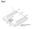
- FIG. 2 is a perspective view of a sub-mount equipped in the optical module shown in FIG. 1.
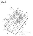
- FIG. 3 is a perspective view of a fiber fixing member equipped in the optical module of FIG. 1.
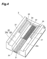
- FIG. 4 is a perspective view showing the state wherein optical fibers are fixed to the fiber fixing member shown in FIG. 3.
- FIG. 5 is a sectional front view taken on line I-I of the optical module shown in FIG. 1.
- FIG. 6 is a sectional side view showing an arrangement example of a passive alignment type optical module.
- FIG. 7 is a sectional view showing an arrangement example of a conventional passive alignment type optical module.
- FIG. 1 is a sectional side view showing the arrangement of an embodiment of the present invention's optical module.
- FIG. 1 shows the cross-sectional view in the plane containing the optical axes of one set among four sets of the optical fiber and the optical semiconductor element. In FIG. 1, the left-to-right direction is the direction of optical transmission along the optical axis of the optical fiber.
- the present optical module is equipped with a circuit substrate 41, a sub-mount 1, a fiber fixing member 2, and a coated optical fiber array 31.
- the circuit substrate 41 is a mounting substrate on which sub-mount 1 is mounted. Wirings, electronic circuits, etc., necessary for signal processing are also mounted on the circuit substrate 41.
- a pre-amplifier 43 which amplifies and outputs an electrical signal, is mounted on the circuit substrate 41.
- the sub-mount 1 is a substrate for installing the optical semiconductor element. This sub-mount 1 is set on the circuit substrate 41.
- the surface of the sub-mount 1 at the side opposite the side of the circuit substrate 41 is an optical element mounting surface (first surface) 16 on which the optical semiconductor element is disposed.
- a silicon substrate may be used as the substrate of the sub-mount 1.
- a photodiode array 11 is disposed on the optical element mounting surface 16.
- This photodiode array 11 is an optical semiconductor element array, with which four photodiodes (photodetecting elements) 12 are arrayed at a fixed pitch as the optical semiconductor elements. These photodiodes 12 are disposed with a direction perpendicular to the optical axes of the optical fibers 3 to be described later (the direction perpendicular to the paper surface in FIG. 1) as the array direction.
- the pre-amp 43 on the circuit substrate 41, the photodiode array 11 on the sub-mount 1, and the electrodes, wirings, etc., disposed on the circuit substrate 41 and sub-mount 1 are electrically connected by die-bonding or wire-bonding, etc.
- the fiber fixing member 2 is a member that fixes the optical fibers. With respect to the sub-mount 1, this fiber fixing member 2 is installed at the side opposite the side of the circuit substrate 41.
- the surface of the fiber fixing member 2 that faces the optical element mounting surface 16 of the sub-mount 1 is an optical fiber fixing surface (second surface) 26 to which the optical fibers are fixed.
- the fiber fixing member 2 may, for example, be molded integrally from resin.
- V-grooves 21 are formed in parallel as fixing grooves for aligning and fixing the optical fibers.
- the coated optical fiber array 31, having four optical fibers arrayed at a fixed pitch, is installed with respect to the V-grooves 21.
- the coating is removed across a predetermined length at a front end portion of the coated optical fiber array 31, thereby exposing four optical fibers 3. These exposed optical fibers 3 are aligned and fixed, respectively, in the corresponding V-grooves 21.
- V-grooves 21 and optical fibers 3 that are fixed to the V-grooves 21 are arrayed in a direction perpendicular to the optical axes of the optical fibers 3 and are positioned at the same pitch as the photodiodes 12 so as to correspond thereto.
- the fiber fixing member 2 is provided with an array housing portion 2b, which protrudes in the direction in which the coated optical fiber array 31 extends from the sub-mount 1 and the optical fiber fixing portion 2a.
- concave mirrors 22 are disposed at positions on the optical axes and opposing the end faces, respectively, of the optical fibers 3. These concave mirrors 22 are provided, respectively, for the four V-grooves 21 and optical fibers 3.
- the concave mirrors 22 are also positioned on the upwardly directed optical axes of the corresponding photodiodes 12 as viewed from the sub-mount 1.
- Each concave mirror 22 converts the optical path of the light emitted from the end face of an optical fiber 3 vertically downward by substantially 90°, converts the light to parallel light, and guides the light while converging it toward a photodiode 12.
- ball lenses 14 are aligned so that their optical axes are matched to the optical axes of the photodiodes 12.
- Each ball lens 14 converges the light, emitted from the optical fiber 3 and converted in the optical path by the concave mirror 22, onto the corresponding photodiode 12.
- a light guiding optical system between the optical fibers 3 and photodiodes 12 is arranged by the concave mirrors 22 and ball lenses 14.
- the ball lenses 14 can be aligned, for example, by fixing onto lens mounting pedestals formed using resist, etc., in the same semiconductor process as the photodiode array 11.
- circuit substrate 41, sub-mount 1, fiber fixing member 2, etc. are housed in a casing 45, comprising a casing body portion 44a, and a casing cover portion 44b positioned above the casing body portion 44a.
- the circuit substrate 41 is disposed with the surface, at the side opposite the surface on which the sub-mount 1 is mounted, facing the bottom portion 45a.
- An opening 47 is provided on the optical axes of the optical fibers 3 at a side portion 45b, which, among the side portions of the casing 45, is at the array housing portion 2b side as viewed from the optical fiber fixing portion 2a.
- the coated optical fiber array 31 is passed through this opening 47.
- the opening 47, through which the coated optical fiber array 31 is passed, is filled with a solder 48.
- This solder 48 fixes the coated optical fiber array 31 to the casing 45 and closes the opening 47 and thereby keeps the casing 45 airtight.
- the use of a metal coating, such as that of a metallized fiber, is preferable as the coating of the coated optical fiber array 31.
- the coated optical fiber array 31 may be fixed to the casing 45 by a resin, etc.
- output terminals 42 At a side portion 45c of the casing 45 that opposes the side portion 45b is inserted output terminals 42. These output terminals 42 guide, to the exterior of the casing, the electrical signals from the photodiodes 12 that have been amplified by the pre-amps 43.
- FIG. 2 is a perspective view of the sub-mount 1 as viewed from the side of the fiber fixing member 2. The arrangement of the sub-mount 1 shall now be described in detail using FIG. 2.
- the guide grooves 10 are for aligning the optical fibers 3 and photodiodes 12 by passive alignment.
- the direction in which these guide grooves 10 are formed is perpendicular to the array direction of the photodiodes 12.
- the guide grooves 10 are disposed at predetermined positions corresponding to second alignment portions equipped on the fiber fixing member 2.
- the cross-sectional shape in the plane perpendicular to the longitudinal direction of each guide groove 10 is a tapered shape that becomes gradually narrow in width from the optical element mounting surface 16 toward the inner side of the sub-mount 1.
- an aligning mark 13 which aligning mark 13 serves as a reference in aligning and fixing the photodiode array 11 with respect to the sub-mount 1.
- the aligning mark 13 is aligned with respect to the two guide grooves 10 and is preferably formed by the same mask process as the guide grooves 10.
- the photodiode array 11 is installed at a position at the upstream side in the optical transmitting direction of the optical fibers 3.
- the photodiode array 11 can be fixed to the sub-mount 1, for example, by flip-chip bonding.
- the Guide grooves 10, which are the first alignment portions, are aligned with respect to the photodiode array 11.
- FIG. 3 is a perspective view of the fiber fixing member 2 as viewed form the sub-mount 1 side. The arrangement of the fiber fixing member 2 shall now be described in detail using FIG 3.
- two guide rails 20, which extend in parallel to each other, are formed as second alignment portions.
- the guide rails 20 are fitted with the guide grooves 10 to align the optical fibers 3 and photodiodes 12 by passive alignment.
- the cross-sectional shape in the plane perpendicular to the longitudinal direction of each guide rail 20 is a tapered shape that becomes gradually narrow in width from the optical fiber fixing surface 26 toward the sub-mount 1 side.
- the direction in which the guide rails 20 are formed is parallel to the direction in which the V-grooves 21 are formed.
- the optical fiber fixing surface 26 is formed so that as viewed in the array direction of the optical fibers 3, which is a direction perpendicular to the optical transmitting direction, the central portion is depressed along the optical transmitting direction.
- This depressed portion is a V-groove forming portion 26a at which the V-grooves 21 for fixing the optical fibers 3 are formed.
- the upstream side portion in the optical transmitting direction of the V-groove forming portion 26a is the array housing portion 2b, and the downstream side portion is the optical fiber fixing portion 2a.
- the upstream side portion in the optical transmitting direction of the V-groove forming portion 26a is the array housing portion 2b, and the downstream side portion is the optical fiber fixing portion 2a.
- four V-grooves 21, extending along the optical transmitting direction, are formed in the optical fiber fixing portion 2a, and four concave mirrors 22 are disposed further at the downstream side.
- the respective sides of the V-groove forming portion 26a are guide rail forming portions 26b.
- the two above-mentioned guide rails 20 are disposed, respectively, at the guide rail forming portions 26b at the respective sides so as to sandwich the four V-grooves 21 formed at the V-groove forming portion 26a.
- the guide rails 20, which are the second alignment portions, are aligned with respect to the V-grooves 21, and the optical fibers 3 fixed to the V-grooves 21.
- the guide portions 27 protrude toward the side at which the sub-mount 1 is positioned as viewed from the optical fiber fixing surface 26 and are the portions that guide the fitting of the guide rails 20 with the guide grooves 10 in the process of aligning and fixing the fiber fixing member 2 with respect to the sub-mount 1.
- the height of protrusion of these guide portions 27 is set smaller than the height of the sub-mount 1.
- FIG. 4 is a perspective view showing the state wherein the coated optical fiber array 31 and optical fibers 3 are fixed to the fiber fixing member 2 shown in FIG. 3. As shown in FIG. 4, the optical fibers 3 are fixed, respectively, to the four V-grooves 21. This fixing is carried out by placing the optical fibers 3 in the V-grooves 21 and adhesively fixing by an adhesive agent. In the process of fixing, a glass plate, etc., may be used as a fiber holder.
- FIG. 5 is a sectional front view taken on line I-I of the optical module shown in FIG. 1.
- the fiber fixing member 2 is set so that its guide portions 27 sandwich the sub-mount 1 from both sides and guide rail forming portions 26b of the optical fiber fixing surface 26 of the fiber fixing member 2 contacts the optical element mounting surface 16 of the sub-mount 1.
- the guide grooves 10, formed in the sub-mount 1 and guide rails 20, formed on the fiber fixing member 2 fit together.
- the photodiodes 12, which are aligned with respect to the guide grooves 10, and optical fibers 3, which are aligned with respect to the guide rails 20, are thereby aligned by passive alignment.
- the fiber fixing member 2 and circuit substrate 41, below the sub-mount 1, are fixed by an adhesive agent.
- an adhesive agent 46 which is filled between the lower surface of the guide portions 27 of the fiber fixing member 2 and the upper surface of the circuit substrate 41, is shown.
- the circuit substrate 41 is mounted to the casing body portion 44a.
- the sub-mount 1 and pre-amps 43 are furthermore mounted to the circuit substrate 41.
- the mounting can be performed by die-bonding by a resin or wire-bonding by gold wires or aluminum wires, etc.
- the optical fibers 3 are fixed to the fiber fixing member 2.
- the fiber fixing member 2, to which the optical fibers 3 are fixed is aligned and fixed with respect to the sub-mount 1.
- adhesive agent 46 is filled in the predetermined spaces to adhesively fix the fiber fixing member 2 to the circuit substrate 41.
- the optical fibers 3 and photodiodes 12 are aligned by the fitting together of the guide grooves 10 of the sub-mount 1 and guide rails 20 of the fiber fixing member 2. Alignment by passive alignment is thus realized with the present optical module.
- guide grooves 10 are used as first alignment portions and guide rails 20 are used as second alignment portions.
- the optical fibers 3 and photodiodes 12 are thus aligned at high precision.
- Guide rails may be used instead as the first alignment portions formed on the sub-mount 1, and guide grooves may be used as the second alignment portions formed on the fiber fixing member 2.
- the optical fiber fixing surface 26 is disposed so as to oppose the optical element mounting surface 16, the step of aligning and fixing the fiber fixing member 2, to which the optical fibers 3 are fixed, with respect to the sub-mount 1 can be performed after the step of die-bonding or wire-bonding, etc., the sub-mount 1 to the circuit substrate 41. Handling and automation of the step of die-bonding or wire-bonding, etc., the sub-mount 1 to the circuit substrate 41 will thus not be hindered.
- the present optical module thus enables mass production and cost reduction. Also, with the present optical module, since the optical fibers 3 are disposed parallel to the optical element mounting surface 16 of the sub-mount 1, the module height is kept low.
- the concave mirrors 22 are provided as the light guiding optical system between the optical fibers 3 and photodiodes 12. Since light emitted from the optical fibers 3 are thereby converged and guided to the photodiodes 12, a high optical coupling factor is realized.
- the concave mirrors 22 make the light from the optical fibers 3 parallel light. Since the light from optical fibers 3 thus propagate as parallel light along the optical paths from the concave mirrors 22 to the ball lenses 14, the tolerance of the optical module is relaxed. For example, calculations using an optical simulator have shown that optical coupling is enabled even when the positional relationship between the concave mirrors 22 and photodiodes 12 is moved by approximately ⁇ 40 ⁇ m.
- the concave mirrors 22 are not necessarily limited to those that convert the reflected light into parallel light.
- optical module since pluralities of the optical fibers 3 and photodiodes 12 are provided, respectively, a plurality of optical signals can be transmitted in parallel. An optical module, enabling high-speed, high-volume transmission, is thus realized.
- the ball lenses 14 for converging light are disposed between the photodiodes 12 and concave mirrors 22.
- a high optical coupling factor is thus realized.
- the ball lenses 14 do not have to be provided.
- Such cases include the case where single mode fibers with a core diameter of 10 ⁇ m are used as the optical fibers 3 and the case where the photodiodes 12 that are used have an adequately large photodetecting diameter.
- the ball lenses 14 can be aligned by fixing onto lens mounting pedestals formed using a resist, etc., in the same semiconductor process as that of the photodiode array 11.
- the ball lenses 14 can thereby be aligned at a precision of within ⁇ 1 to 2 ⁇ m in this case.
- the aligning mark 13 can be aligned at a precision of within ⁇ 1 to 2 ⁇ m with respect to the guide grooves 10.
- the photodiode array 11 and guide grooves 10 can be aligned at high precision with respect to each other.
- the photodiode array 11 can be prepared from the same material and by the same semiconductor process as the sub-mount 1 and thereby formed to be monolithic to the guide grooves 10.
- the photodiode array 11 and guide grooves 10 are aligned at high precision with respect to each other when formed in this manner as well. In this case, the aligning mark 13 need not be formed as it is unnecessary.
- alignment can be performed at a precision of within ⁇ 5 ⁇ m.
- the fiber fixing member 2 is integrally molded from resin, it can be prepared at a high precision wherein the precision of the respective pitches of the V-grooves 21 and concave mirrors 22, the relative positional relationship of the V-grooves 21 and concave mirrors 22, and relative positional relationship of the guide rails 20 and V-grooves 21 are within ⁇ 10 ⁇ m.
- the fiber fixing member 2 may also be molded integrally using an MIM (Metal Injection Mold). With this type of molding, the precision can be made as high as in the case of integral molding from resin.
- MIM Metal Injection Mold
- an adhesive agent having a refractive index matching characteristic can be filled between the optical fibers 3 and concave mirrors 22. The returning light from the front ends of the optical fibers 3 can thereby be restrained.
- the guide rails 20 are formed substantially parallel to the V-grooves 21.
- the guide rails 20 and V-grooves 21 can thus be aligned and formed readily.
- the guide rails 20 are formed, respectively, on the guide rail forming portions 26b at the respective sides of the V-grooves 21, sub-mount 1 and the fiber fixing member 2 are aligned at high precision.
- the cross-sectional shapes in the plane perpendicular to the longitudinal direction of the guide grooves 10 and guide rails 20 are tapered shapes.
- the guide grooves 10 and guide rails 20 can thus be fitted together readily.
- the fiber fixing member 2 is provided with the guide portions 27, the fitting of the guide grooves 10 and guide rails 20 can be performed readily in a single step.
- Optical modules with which optical fibers and optical semiconductor elements are aligned by the fitting of guide rails and guide grooves, are also described in Japanese Patent Application Laid-Open No. H7-77634 and Japanese Patent Application Laid-Open No. H7-151940.
- this optical module has an arrangement wherein the optical fibers and the optical semiconductor elements are positioned along the same optical axis.
- portions for mounting the optical semiconductor elements must be provided on the substrate and along the optical axis in addition to the fixing portions for the optical fibers. This optical module thus cannot be made compact.
- the present invention's optical module has an arrangement wherein, the concave mirrors 22, which convert the optical paths of the light emitted from the optical fibers 3, are provided and the light from the optical fibers 3 are made incident on the photodiodes 12 at positions opposing the optical fiber fixing surface 26. There is thus no need to provide portions for mounting the photodiodes 12 on the fiber fixing member 2.
- the present optical module can thus be made compact.
- an optical module wherein an alignment substrate is provided in addition to a fiber fixing member and a sub-mount.
- an alignment portion must be formed not just on the fiber fixing member 2 and sub-mount but on the substrate as well.
- the step of forming the alignment portions and thus the process of manufacturing the entire optical module becomes complicated. Also, since there are two independent locations where alignment portions fit with each other (that is, the two locations for the fitting of the fiber fixing member with the substrate and the fitting of the sub-mount with the substrate), alignment errors will be amplified.
- alignment portions 10 and 20 are provided just at the sub-mount 1 and fiber fixing member 2 and these are fitted directly to perform alignment.
- this optical module the manufacturing process is simplified and alignment is carried out at high precision.
- FIG. 6 As a passive alignment type optical module, the arrangement shown in FIG. 6 may be considered for example.
- the alignment of an optical fiber 82 and an optical semiconductor element 84 is carried out by means of a V-groove and an aligning mark that have been formed on a substrate 81 by the same mask process.
- a planar mirror 85, which guides light between the optical fiber 82 and optical semiconductor element 84 is provided on the substrate 81.
- optical module since the optical fiber 82 enters below the optical semiconductor element 84, the optical semiconductor element 84 is flip-chip mounted using the alignment mark as a guide after adhesively fixing the optical fiber 82 in the V-groove. Handling and automation in the step of flip-chip mounting the optical semiconductor element 84 are thus hindered. This optical module thus does not enable mass production and cost reduction.
- the fiber fixing member 2, to which the optical fibers 3 have been fixed can be aligned and fixed with respect to the sub-mount 1 after die-bonding or wire-bonding, etc., the sub-mount 1 to the circuit substrate 41.
- This optical module can thus be mass-produced and reduced in cost.
- the rear surface (the surface at the side opposite the photodetecting surface) of the optical semiconductor element 84 is floated. Heat thus cannot be dissipated efficiently from the optical semiconductor element 84. This becomes a cause of unstable operation of the optical module, especially in the case of a VCSEL (Vertical Cavity Surface Emitting Laser) or other element of high heat generation amount.
- VCSEL Vertical Cavity Surface Emitting Laser
- the optical coupling factor is low since a concave mirror or other converging optical system is not used. That is, when high-speed operation of approximately 2.5Gbps is considered, an element with a photodetecting diameter of 40 to 80 ⁇ m is normally used as the optical semiconductor element 84 or 94. Meanwhile, the distance along the optical axis from the optical fiber 82 or 92 to the optical semiconductor element 84 or 94 must be set to no less than the fiber cladding diameter (125 ⁇ m) in the case of the arrangement of FIG. 6 and no less than the loop height (approximately 100 ⁇ m) of the wires used in bonding in the case of the arrangement of FIG. 7.
- the spot diameter on the optical semiconductor element 84 or 94 will be 117.5 ⁇ m in the case of a core diameter of 62.5 ⁇ m and a numerical aperture of 0.275 and will be 92 ⁇ m in the case of a core diameter of 50 ⁇ m, and thus the total light amount cannot be detected by the optical semiconductor element 84 or 94.
- the optical coupling factor will be lowered especially in the case where a multimode fiber of large core diameter and numerical aperture is used.
- each of the optical fibers 3 a multimode fiber with a core diameter of 62.5 ⁇ m and a numerical aperture of 0.275 is used, and as each of the photodiodes 12, a photodiode, having a photodetecting diameter of 80 ⁇ m and enabled to perform high-speed operation of up to 2.5Gbps, is used. Also, the array pitch of the photodiodes 12 in the photodiode array 11 is 250 ⁇ m.
- the spreading of the light flux must be restrained to be no more than 200pm in consideration of a margin.
- the upper limit of the interval between the optical fibers 3 and concave mirrors 22 is thus 250 ⁇ m.
- the interval between the concave mirrors 22 and photodiodes 12 must be set to no less than 250 ⁇ m in consideration of space for bonding wires, even if the ball lenses 14 are not to be provided.
- the interval between the concave mirrors 22 and photodiodes 12 must be set to no less than 312.5 ⁇ m. In the case where a glass plate, etc., is provided as an optical fiber holder, since the thickness thereof must be considered, the lower limit of the above-mentioned interval will be greater than 312.5 ⁇ m.
- the interval between the concave mirrors 22 and photodiodes 12 will be greater than the interval between the optical fibers 3 and concave mirrors 22 and the optical system will be a magnifying system.
- the magnification will be 1.25 and the image of a core of 62.5 ⁇ m diameter will be an image of 78 ⁇ m diameter on a photodiode 12.
- the photodetecting diameter of each photodiode 12 is 80 ⁇ m, in consideration of the tolerances of the manufacture and assembly of the respective members 1 and 2, it will be difficult to realize an optical coupling factor of 100%.
- the present optical module by providing a converging optical system of the concave mirrors 22, etc., the light from the optical fibers 3 are guided to the photodiodes 12 upon being converged. An optical coupling factor of 100% can thus be realized with this optical module.
- N which expresses the number of the optical fibers 3, the number of the photodiodes 12, etc.
- this number N may be set as suited.
- N is set to 2 or more, since a plurality of optical signals can be transmitted in parallel as described above, transmission at higher speed and greater volume is enabled. Even when N is set to 1, the same effects as the optical module shown in FIG. 1 to FIG. 5 are exhibited in regard to the alignment of the optical fiber 3 and photodiode 12, etc.
- a photodetecting element besides photodiode 12 may be used, or a light emitting element, such as a VCSEL, may be used.
- a light emitting element such as a VCSEL
- the concave mirror 22 guides the light emitted from the light emitting element to the optical fiber 3 and the ball lens 14 converges the light emitted from the light emitting element.
- the present invention's optical module can be used as an optical module suitable for mass production and cost reduction. That is, with the present invention's optical module, the optical fiber and the optical semiconductor element are aligned by the fitting together of the first alignment portion and the second alignment portion. Alignment of the optical fiber and optical semiconductor element by passive alignment is thus realized.
- the optical fiber and the optical semiconductor element are aligned at high precision.
- the step of aligning and fixing the fiber fixing member, to which the optical fiber is fixed, with respect to the sub-mount can be performed after the step of die-bonding or wire-bonding, etc., the sub-mount to the circuit substrate.
- An optical module that enables mass production and cost reduction is thus realized. Also, since the optical fiber is disposed in parallel to the first surface of the sub-mount, the module height is kept low.
- the concave mirror is disposed as the light guiding optical system between the optical fiber and the optical semiconductor element. Since the light emitted from one of either of the optical fiber and the optical semiconductor element is thereby converged and guided to the other, a high optical coupling factor is realized.
Landscapes
- Physics & Mathematics (AREA)
- General Physics & Mathematics (AREA)
- Optics & Photonics (AREA)
- Optical Couplings Of Light Guides (AREA)
- Light Receiving Elements (AREA)
- Semiconductor Lasers (AREA)
Applications Claiming Priority (3)
| Application Number | Priority Date | Filing Date | Title |
|---|---|---|---|
| JP2003041472A JP3947481B2 (ja) | 2003-02-19 | 2003-02-19 | 光モジュール及びその製造方法 |
| JP2003041472 | 2003-02-19 | ||
| PCT/JP2004/001926 WO2004074896A1 (ja) | 2003-02-19 | 2004-02-19 | 光モジュール |
Publications (2)
| Publication Number | Publication Date |
|---|---|
| EP1596233A1 true EP1596233A1 (de) | 2005-11-16 |
| EP1596233A4 EP1596233A4 (de) | 2007-05-23 |
Family
ID=32905288
Family Applications (1)
| Application Number | Title | Priority Date | Filing Date |
|---|---|---|---|
| EP04712756A Withdrawn EP1596233A4 (de) | 2003-02-19 | 2004-02-19 | Optisches modul |
Country Status (7)
| Country | Link |
|---|---|
| US (1) | US7254301B2 (de) |
| EP (1) | EP1596233A4 (de) |
| JP (1) | JP3947481B2 (de) |
| KR (1) | KR101074593B1 (de) |
| CN (1) | CN100401121C (de) |
| TW (1) | TWI298398B (de) |
| WO (1) | WO2004074896A1 (de) |
Cited By (2)
| Publication number | Priority date | Publication date | Assignee | Title |
|---|---|---|---|---|
| EP1967878A4 (de) * | 2005-12-28 | 2009-12-23 | Omron Corp A Corp Of Japan | Optisches modul |
| EP2753964B1 (de) * | 2011-09-07 | 2020-10-07 | The Boeing Company | Hermetische verpackung mit kleinem formfaktor für optische vorrichtungen für kunststoffglasfasernetzwerke |
Families Citing this family (28)
| Publication number | Priority date | Publication date | Assignee | Title |
|---|---|---|---|---|
| US7177504B2 (en) * | 2004-09-30 | 2007-02-13 | Intel Corporation | Manufacturable connectorization process for optical chip-to-chip interconnects |
| JP4929821B2 (ja) * | 2006-04-27 | 2012-05-09 | オムロン株式会社 | 光伝送モジュール |
| JP4189692B2 (ja) | 2006-07-07 | 2008-12-03 | セイコーエプソン株式会社 | 光モジュール用パッケージおよび光モジュール |
| JP2009042400A (ja) * | 2007-08-07 | 2009-02-26 | Omron Corp | フィルム光導波路パッケージ、フィルム光導波路モジュールおよび電子機器 |
| DE102007053849A1 (de) | 2007-09-28 | 2009-04-02 | Osram Opto Semiconductors Gmbh | Anordnung umfassend ein optoelektronisches Bauelement |
| EP2528495B1 (de) * | 2010-01-25 | 2018-03-28 | Axsun Technologies, Inc. | Siob-oct-sonde für medizinische bildgebung |
| US9046668B2 (en) * | 2011-06-22 | 2015-06-02 | Panasonic Intellectual Property Management Co., Ltd. | Optical module |
| JP5847473B2 (ja) * | 2011-07-21 | 2016-01-20 | シチズンホールディングス株式会社 | 光モジュール |
| TWI463204B (zh) * | 2011-11-18 | 2014-12-01 | Universal Microelectronics Co Ltd | 光機總成及其製作方法 |
| US20160274318A1 (en) * | 2012-03-05 | 2016-09-22 | Nanoprecision Products, Inc. | Optical bench subassembly having integrated photonic device |
| US20130294732A1 (en) * | 2012-03-05 | 2013-11-07 | Nanoprecision Products, Inc. | Hermetic optical fiber alignment assembly having integrated optical element |
| US20160377821A1 (en) * | 2012-03-05 | 2016-12-29 | Nanoprecision Products, Inc. | Optical connection of optical fibers to grating couplers |
| WO2014011282A2 (en) * | 2012-04-11 | 2014-01-16 | Nanoprecision Products, Inc. | Hermetic optical fiber alignment assembly |
| US9243784B2 (en) | 2012-12-20 | 2016-01-26 | International Business Machines Corporation | Semiconductor photonic package |
| TWI506318B (zh) * | 2012-12-26 | 2015-11-01 | Hon Hai Prec Ind Co Ltd | 光纖耦合連接器 |
| US9400356B2 (en) | 2013-03-14 | 2016-07-26 | International Business Machines Corporation | Fiber pigtail with integrated lid |
| WO2014141458A1 (ja) * | 2013-03-15 | 2014-09-18 | 株式会社日立製作所 | 光モジュールおよび伝送装置 |
| US20140355934A1 (en) * | 2013-05-29 | 2014-12-04 | Avago Technologies General Ip (Singapore) Pte. Ltd. | Optics system for use in a parallel optical communications module |
| CN204009138U (zh) * | 2014-01-16 | 2014-12-10 | 中兴通讯股份有限公司 | 一种光耦合器件和光耦合单元 |
| CN106104344B (zh) * | 2014-03-24 | 2017-11-10 | 西铁城时计株式会社 | 光纤的安装零件、光模块以及制造方法 |
| CN104459906A (zh) * | 2014-10-21 | 2015-03-25 | 华天科技(昆山)电子有限公司 | 用于有源光缆光学系统的无源对准结构及加工工艺 |
| US9348094B1 (en) | 2015-03-21 | 2016-05-24 | Skorpios Technologies, Inc. | Axial alignment of a lensed fiber in a silica v-groove |
| CN105607196B (zh) * | 2015-12-30 | 2018-05-22 | 华进半导体封装先导技术研发中心有限公司 | 一种光学芯片、制备方法及应用该光学芯片的光互连模块 |
| US10534143B1 (en) | 2018-09-20 | 2020-01-14 | Waymo Llc | Methods for optical system manufacturing |
| KR20210087995A (ko) | 2018-11-08 | 2021-07-13 | 맥스웰 테크놀러지스 인코포레이티드 | 염 및/또는 폼을 포함하는 에너지 저장 장치를 위한 조성물 및 방법 |
| CN111323878B (zh) * | 2020-04-01 | 2021-10-15 | 联合微电子中心有限责任公司 | 一种激光器芯片与硅基光电子芯片的耦合对准装置及方法 |
| JP2022061168A (ja) * | 2020-10-06 | 2022-04-18 | 住友電気工業株式会社 | 光コネクタケーブル、及び光コネクタケーブルの製造方法 |
| TWM636164U (zh) * | 2022-09-14 | 2023-01-01 | 上詮光纖通信股份有限公司 | 光學元件組裝對準結構 |
Family Cites Families (22)
| Publication number | Priority date | Publication date | Assignee | Title |
|---|---|---|---|---|
| JPH01183606A (ja) * | 1988-01-18 | 1989-07-21 | Fujitsu Ltd | 受光デバイス |
| US4897711A (en) * | 1988-03-03 | 1990-01-30 | American Telephone And Telegraph Company | Subassembly for optoelectronic devices |
| JPH0339706A (ja) * | 1989-07-06 | 1991-02-20 | Fujitsu Ltd | 光モジュール |
| US5071213A (en) * | 1990-10-31 | 1991-12-10 | The Boeing Company | Optical coupler and method of making optical coupler |
| JP3342949B2 (ja) * | 1994-05-06 | 2002-11-11 | 株式会社リコー | 光モジュール |
| JPH0777634A (ja) | 1993-09-09 | 1995-03-20 | Fujitsu Ltd | 光端末装置 |
| JPH07151940A (ja) * | 1993-11-29 | 1995-06-16 | Fujitsu Ltd | 光結合構造とその製造方法 |
| JPH07249798A (ja) * | 1994-03-09 | 1995-09-26 | Fujitsu Ltd | 光部品固定装置及びその製造方法 |
| JP3150070B2 (ja) | 1996-09-30 | 2001-03-26 | 日本電気株式会社 | 受光モジュール及びその製造方法 |
| JP2001507814A (ja) * | 1996-12-31 | 2001-06-12 | ハネウエル・インコーポレーテッド | フレキシブル光コネクタアセンブリ |
| JP3403306B2 (ja) | 1997-01-17 | 2003-05-06 | 古河電気工業株式会社 | 光モジュール |
| KR19980066890A (ko) * | 1997-01-29 | 1998-10-15 | 김광호 | 광도파로와 광섬유 결합장치 및 방법 |
| DE19709842C1 (de) | 1997-02-28 | 1998-10-15 | Siemens Ag | Elektrooptische Koppelbaugruppe |
| JPH10339824A (ja) * | 1997-06-06 | 1998-12-22 | Sumitomo Electric Ind Ltd | 光モジュール用プラットフォームとその製造方法 |
| US5980360A (en) | 1998-05-06 | 1999-11-09 | Gerber Coburn Optical, Inc. | Method and apparatus for performing work operations on a surface of one or more lenses |
| US6187515B1 (en) * | 1998-05-07 | 2001-02-13 | Trw Inc. | Optical integrated circuit microbench system |
| DE19861162A1 (de) * | 1998-11-06 | 2000-06-29 | Harting Elektrooptische Bauteile Gmbh & Co Kg | Verfahren zur Herstellung einer Leiterplatte sowie Leiterplatte |
| JP2000275472A (ja) * | 1999-03-26 | 2000-10-06 | Fujitsu Ltd | 光導波路付基板と該基板を用いる光モジュール装置 |
| JP2001051162A (ja) * | 1999-06-04 | 2001-02-23 | Nippon Telegr & Teleph Corp <Ntt> | 光結合部品 |
| DE19932430C2 (de) * | 1999-07-12 | 2002-03-14 | Harting Elektrooptische Bauteile Gmbh & Co Kg | Opto-elektronische Baugruppe sowie Bauteil für diese Baugruppe |
| JP4828015B2 (ja) * | 2000-07-13 | 2011-11-30 | 三菱電機株式会社 | 光モジュール作製方法 |
| JP3791394B2 (ja) * | 2001-11-01 | 2006-06-28 | 日本電気株式会社 | 光導波路基板 |
-
2003
- 2003-02-19 JP JP2003041472A patent/JP3947481B2/ja not_active Expired - Fee Related
-
2004
- 2004-02-19 WO PCT/JP2004/001926 patent/WO2004074896A1/ja not_active Ceased
- 2004-02-19 EP EP04712756A patent/EP1596233A4/de not_active Withdrawn
- 2004-02-19 US US10/546,187 patent/US7254301B2/en not_active Expired - Fee Related
- 2004-02-19 CN CNB2004800047252A patent/CN100401121C/zh not_active Expired - Fee Related
- 2004-02-19 TW TW093104070A patent/TWI298398B/zh not_active IP Right Cessation
- 2004-02-19 KR KR1020057014716A patent/KR101074593B1/ko not_active Expired - Fee Related
Cited By (2)
| Publication number | Priority date | Publication date | Assignee | Title |
|---|---|---|---|---|
| EP1967878A4 (de) * | 2005-12-28 | 2009-12-23 | Omron Corp A Corp Of Japan | Optisches modul |
| EP2753964B1 (de) * | 2011-09-07 | 2020-10-07 | The Boeing Company | Hermetische verpackung mit kleinem formfaktor für optische vorrichtungen für kunststoffglasfasernetzwerke |
Also Published As
| Publication number | Publication date |
|---|---|
| JP3947481B2 (ja) | 2007-07-18 |
| TW200428057A (en) | 2004-12-16 |
| JP2004264362A (ja) | 2004-09-24 |
| KR101074593B1 (ko) | 2011-10-17 |
| CN100401121C (zh) | 2008-07-09 |
| US7254301B2 (en) | 2007-08-07 |
| EP1596233A4 (de) | 2007-05-23 |
| KR20050100390A (ko) | 2005-10-18 |
| CN1751256A (zh) | 2006-03-22 |
| TWI298398B (en) | 2008-07-01 |
| WO2004074896A1 (ja) | 2004-09-02 |
| US20060233497A1 (en) | 2006-10-19 |
Similar Documents
| Publication | Publication Date | Title |
|---|---|---|
| US7254301B2 (en) | Optical module | |
| US8079125B2 (en) | Manufacturing method of multi-channel optical module | |
| US6913400B2 (en) | Optoelectric module for multi-fiber arrays | |
| KR100411577B1 (ko) | 광섬유 접속부 및 그것의 사용 방법 | |
| US6901221B1 (en) | Method and apparatus for improved optical elements for vertical PCB fiber optic modules | |
| US6748143B2 (en) | Optical transceiver module and optical communications system using the same | |
| US5781682A (en) | Low-cost packaging for parallel optical computer link | |
| US6374021B1 (en) | Light transmitting/receiving module | |
| CN112838897B (zh) | 一种光模块 | |
| JP2010122312A (ja) | 送受信レンズブロック及びそれを用いた光モジュール | |
| CN113835165B (zh) | 一种光发射组件、芯片、光模块及光通信设备 | |
| JP2006506657A (ja) | 光ファイバーとの半導体装置の能動的光学整合のための一体化プラットホーム | |
| KR100627701B1 (ko) | 병렬 광접속 모듈 | |
| JP2019184941A (ja) | 光サブアセンブリ及びその製造方法並びに光モジュール | |
| JP2010122311A (ja) | レンズブロック及びそれを用いた光モジュール | |
| JP2004212847A (ja) | 光結合器 | |
| US7430375B2 (en) | Optical transceiver | |
| CN112929092B (zh) | 一种光模块 | |
| CN214228256U (zh) | 一种光模块 | |
| US20020136504A1 (en) | Opto-electronic interface module for high-speed communication systems and method of assembling thereof | |
| CA2359002C (en) | Optoelectric module for multi-fiber arrays | |
| CN214228255U (zh) | 一种光模块 | |
| Sunaga et al. | 2 Gbit/s small form factor fiber-optic transceiver for single mode optical fiber | |
| KR100398045B1 (ko) | 광 송수신 모듈 |
Legal Events
| Date | Code | Title | Description |
|---|---|---|---|
| PUAI | Public reference made under article 153(3) epc to a published international application that has entered the european phase |
Free format text: ORIGINAL CODE: 0009012 |
|
| 17P | Request for examination filed |
Effective date: 20050825 |
|
| AK | Designated contracting states |
Kind code of ref document: A1 Designated state(s): AT BE BG CH CY CZ DE DK EE ES FI FR GB GR HU IE IT LI LU MC NL PT RO SE SI SK TR |
|
| AX | Request for extension of the european patent |
Extension state: AL LT LV MK |
|
| DAX | Request for extension of the european patent (deleted) | ||
| RBV | Designated contracting states (corrected) |
Designated state(s): DE FR GB |
|
| A4 | Supplementary search report drawn up and despatched |
Effective date: 20070420 |
|
| 17Q | First examination report despatched |
Effective date: 20070803 |
|
| STAA | Information on the status of an ep patent application or granted ep patent |
Free format text: STATUS: THE APPLICATION HAS BEEN WITHDRAWN |
|
| 18W | Application withdrawn |
Effective date: 20140829 |