EP1596410A1 - Panneau d'affichage à plasma et son procédé de fabrication - Google Patents
Panneau d'affichage à plasma et son procédé de fabrication Download PDFInfo
- Publication number
- EP1596410A1 EP1596410A1 EP05006482A EP05006482A EP1596410A1 EP 1596410 A1 EP1596410 A1 EP 1596410A1 EP 05006482 A EP05006482 A EP 05006482A EP 05006482 A EP05006482 A EP 05006482A EP 1596410 A1 EP1596410 A1 EP 1596410A1
- Authority
- EP
- European Patent Office
- Prior art keywords
- barrier rib
- pixels
- sub
- plasma display
- display panel
- Prior art date
- Legal status (The legal status is an assumption and is not a legal conclusion. Google has not performed a legal analysis and makes no representation as to the accuracy of the status listed.)
- Withdrawn
Links
- 238000000034 method Methods 0.000 title claims abstract description 37
- 238000004519 manufacturing process Methods 0.000 title claims abstract description 11
- 230000004888 barrier function Effects 0.000 claims abstract description 168
- 238000000638 solvent extraction Methods 0.000 claims abstract description 22
- 239000003989 dielectric material Substances 0.000 claims abstract description 8
- 238000000576 coating method Methods 0.000 claims abstract description 7
- 239000011248 coating agent Substances 0.000 claims abstract description 5
- 230000001788 irregular Effects 0.000 claims abstract description 5
- 239000011521 glass Substances 0.000 claims abstract description 3
- 239000011159 matrix material Substances 0.000 claims description 34
- 239000000463 material Substances 0.000 claims description 15
- OFCNXPDARWKPPY-UHFFFAOYSA-N allopurinol Chemical compound OC1=NC=NC2=C1C=NN2 OFCNXPDARWKPPY-UHFFFAOYSA-N 0.000 claims description 2
- 239000000203 mixture Substances 0.000 abstract description 10
- 238000005192 partition Methods 0.000 abstract description 6
- 239000000758 substrate Substances 0.000 description 27
- 230000008569 process Effects 0.000 description 13
- 238000005488 sandblasting Methods 0.000 description 5
- 239000002245 particle Substances 0.000 description 4
- 239000004576 sand Substances 0.000 description 4
- 230000003247 decreasing effect Effects 0.000 description 3
- 230000000007 visual effect Effects 0.000 description 3
- FYYHWMGAXLPEAU-UHFFFAOYSA-N Magnesium Chemical compound [Mg] FYYHWMGAXLPEAU-UHFFFAOYSA-N 0.000 description 2
- 230000000903 blocking effect Effects 0.000 description 2
- 238000007796 conventional method Methods 0.000 description 2
- 229910000765 intermetallic Inorganic materials 0.000 description 2
- 238000010030 laminating Methods 0.000 description 2
- 238000007639 printing Methods 0.000 description 2
- 230000009467 reduction Effects 0.000 description 2
- 239000011347 resin Substances 0.000 description 2
- 229920005989 resin Polymers 0.000 description 2
- 238000007650 screen-printing Methods 0.000 description 2
- 239000007921 spray Substances 0.000 description 2
- 238000004544 sputter deposition Methods 0.000 description 2
- VYZAMTAEIAYCRO-UHFFFAOYSA-N Chromium Chemical compound [Cr] VYZAMTAEIAYCRO-UHFFFAOYSA-N 0.000 description 1
- OAICVXFJPJFONN-UHFFFAOYSA-N Phosphorus Chemical compound [P] OAICVXFJPJFONN-UHFFFAOYSA-N 0.000 description 1
- 239000000654 additive Substances 0.000 description 1
- 230000000996 additive effect Effects 0.000 description 1
- 239000003086 colorant Substances 0.000 description 1
- 150000001875 compounds Chemical class 0.000 description 1
- 230000002542 deteriorative effect Effects 0.000 description 1
- 230000000694 effects Effects 0.000 description 1
- 238000010292 electrical insulation Methods 0.000 description 1
- AMGQUBHHOARCQH-UHFFFAOYSA-N indium;oxotin Chemical compound [In].[Sn]=O AMGQUBHHOARCQH-UHFFFAOYSA-N 0.000 description 1
- 239000011261 inert gas Substances 0.000 description 1
- 229910052749 magnesium Inorganic materials 0.000 description 1
- 239000011777 magnesium Substances 0.000 description 1
- 229910052751 metal Inorganic materials 0.000 description 1
- 239000002184 metal Substances 0.000 description 1
- 238000012986 modification Methods 0.000 description 1
- 230000004048 modification Effects 0.000 description 1
- 230000003287 optical effect Effects 0.000 description 1
- 238000002161 passivation Methods 0.000 description 1
- 238000000926 separation method Methods 0.000 description 1
- 239000005361 soda-lime glass Substances 0.000 description 1
Images





Classifications
-
- H—ELECTRICITY
- H01—ELECTRIC ELEMENTS
- H01J—ELECTRIC DISCHARGE TUBES OR DISCHARGE LAMPS
- H01J11/00—Gas-filled discharge tubes with alternating current induction of the discharge, e.g. alternating current plasma display panels [AC-PDP]; Gas-filled discharge tubes without any main electrode inside the vessel; Gas-filled discharge tubes with at least one main electrode outside the vessel
- H01J11/10—AC-PDPs with at least one main electrode being out of contact with the plasma
- H01J11/12—AC-PDPs with at least one main electrode being out of contact with the plasma with main electrodes provided on both sides of the discharge space
-
- H—ELECTRICITY
- H01—ELECTRIC ELEMENTS
- H01J—ELECTRIC DISCHARGE TUBES OR DISCHARGE LAMPS
- H01J11/00—Gas-filled discharge tubes with alternating current induction of the discharge, e.g. alternating current plasma display panels [AC-PDP]; Gas-filled discharge tubes without any main electrode inside the vessel; Gas-filled discharge tubes with at least one main electrode outside the vessel
- H01J11/20—Constructional details
- H01J11/34—Vessels, containers or parts thereof, e.g. substrates
- H01J11/36—Spacers, barriers, ribs, partitions or the like
-
- H—ELECTRICITY
- H01—ELECTRIC ELEMENTS
- H01J—ELECTRIC DISCHARGE TUBES OR DISCHARGE LAMPS
- H01J9/00—Apparatus or processes specially adapted for the manufacture, installation, removal, maintenance of electric discharge tubes, discharge lamps, or parts thereof; Recovery of material from discharge tubes or lamps
- H01J9/24—Manufacture or joining of vessels, leading-in conductors or bases
- H01J9/241—Manufacture or joining of vessels, leading-in conductors or bases the vessel being for a flat panel display
- H01J9/242—Spacers between faceplate and backplate
-
- H—ELECTRICITY
- H01—ELECTRIC ELEMENTS
- H01J—ELECTRIC DISCHARGE TUBES OR DISCHARGE LAMPS
- H01J2211/00—Plasma display panels with alternate current induction of the discharge, e.g. AC-PDPs
- H01J2211/20—Constructional details
- H01J2211/34—Vessels, containers or parts thereof, e.g. substrates
- H01J2211/36—Spacers, barriers, ribs, partitions or the like
- H01J2211/361—Spacers, barriers, ribs, partitions or the like characterized by the shape
Definitions
- the present invention relates to a plasma display panel and a manufacture method thereof, and more particularly, to a plasma display panel and a manufacture method thereof in which when the plasma display panel is driven, a color mixture of emitted light can be prevented and a contrast characteristic can be improved.
- plasma display panel (Hereinafter, referred to as "PDP") includes a front substrate and a rear substrate formed of soda-lime glass, and a barrier rib defining one unit cell between the front substrate and the rear substrate.
- inert gas such as He-Xe and He-Ne
- vacuum ultraviolet rays are generated and phosphor is excited between the barrier ribs, thereby displaying an image.
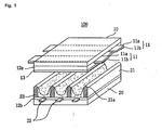
- FIG. 1 is a schematic perspective view illustrating a structure of a conventional plasma display panel.
- a plasma display panel (PDP) 100 includes a front substrate 10 and a rear substrate 20, which are spaced apart and engaged in parallel with each other.
- the front substrate 10 is a display surface on which the image is displayed.
- the rear substrate 20 is a rear surface.
- the front substrate 10 is formed at a lower side of the PDP.
- the front substrate 10 includes a pair of sustain electrodes 11 for sustaining light emission using a mutual discharge in one pixel.
- the sustain electrodes 11 are comprised of a transparent electrode 11 a formed of indium-tin-oxide (ITO) and a bus electrode 11 b formed of metal.
- the sustain electrodes 11 are covered with a dielectric layer 12a, which limits a discharge current and insulates the sustain electrodes.
- a passivation layer 13 is formed of oxide magnesium (MgO) on the dielectric layer 12a to facilitate a discharge.
- the rear substrate 20 includes stripe-type (or well-type) barrier ribs 21 and a plurality of address electrodes 22.
- the stripe-type (or well-type) barrier ribs 21 are arranged in parallel with one another to form a plurality of discharge spaces, that is, a plurality of cells.
- the plurality of address electrodes 22 are arranged in parallel with the barrier ribs 21 to perform an address discharge and generate vacuum ultraviolet rays at their intersection with the sustain electrodes 11.
- a dielectric layer 12b is formed on the address electrodes 22.
- Red (R), green (G), blue (B) phosphors 23 are coated on the dielectric layer 12b to emit a visible ray, thereby displaying the image in the address discharge.
- a method for expressing a gray level in the above constructed PDP is illustrated in FIG. 2.
- FIG. 2 is a view illustrating a conventional method for expressing the gray level in the plasma display panel.
- the gray level is expressed by dividing one frame into several sub-fields each having a different number of light emission times.
- Each of the sub-fields is divided into a reset period for uniformly generating the discharge, an address period for selecting the discharge cell, and a sustain period for expressing the gray level depending on the number of discharge times.
- a frame period (16.6ms) corresponding to 1/60 second is divided into eight sub-fields (SF1 to SF8).
- Each of eight sub-fields is again divided into the reset period, the address period and the sustain period.
- the reset period and the address period are the same at each sub-field.
- the address discharge is generated by a voltage difference between the address electrode (data electrode) and the transparent electrode (scan electrode) to select the discharge cell.
- the unit pixel is constituted of three kinds of sub-pixels emitting R, G, B lights.
- Each of the sub-pixels controls an amount of emitted light depending on the number of the sustain pulses, and visually juxtaposes and mixes the controlled lights, thereby expressing the color and the gray level.
- FIGs. 3A through 3D are views illustrating various discharge cell structures in the conventional plasma display panel.
- FIG. 3A illustrates the discharge cell structure having a stripe-type barrier rib
- FIG. 3B illustrates the discharge cell structure having a well-type barrier rib
- FIG. 3C illustrates the discharge cell structure having a delta-type barrier rib
- FIG. 3D illustrates the discharge cell structure having a honey-type barrier rib.
- a barrier rib 21 separates phosphors expressing each R, G, B color.
- the sub-pixels 101 a, 101b and 101 c constitute a unit pixel 101 with the barrier rib 21 functioning as a boundary.
- the unit pixel is arranged to form a predetermined shape with an adjacent unit pixel using the barrier rib 21 functioning as the boundary, to display the image.
- the barrier rib functions to prevent electrical and optical crosstalk between the sub-pixels or the unit pixels.
- the barrier rib is the most important element in controlling a display quality and a light emission efficiency of the PDP.
- the barrier rib partitioning the unit pixel has the same width as the barrier rib functioning as the boundary between the R, G, B sub-pixels constituting the unit pixel.
- each unit pixel emits light and the emitted light is mixed and displayed, there is a drawback in that a color mixture characteristic depending on a color of the adjacent unit pixel is not good.
- the barrier rib formed between the sub-pixels has the same width as the barrier rib formed between the unit pixels, when the PDP is driven, the color mixture characteristic between an inherent color of the unit pixel and the color of the adjacent unit pixel is deteriorated.
- a black matrix having a low reflectance is formed at the front substrate to separate the colors and decrease a reflectance between upper and lower unit pixels, thereby improving a contrast characteristic.
- FIGs. 4A and 4B are views illustrating black matrix structures disposed at the front substrate in the conventional PDP having the stripe-type discharge cell structure or the well-type discharge cell structure.
- a black matrix 13a is formed only in a traverse direction of the unit pixel 101.
- Such a black matrix structure has a good contrast characteristic due to color separation and reflectance reduction between the unit pixels 101 formed at upper and lower sides on the basis of the black matrix 13a.
- the barrier rib 21 partitioning the unit pixels or the sub-pixels is formed of black-color material having the low reflectance to improve the contrast characteristic.
- such a black matrix structure has a drawback in that since the transparent front substrate is provided at a predetermined thickness between an upper end of the barrier rib and the exterior, the emitted light is not fully blocked between the unit pixels, thereby deteriorating the contrast characteristic.
- an object of the present invention is to solve at least the problems and disadvantages of the background art.
- An object of the present invention is to provide a plasma display panel and a manufacture method thereof in which a barrier rib partitioning a unit pixel is deformed in structure, thereby improving a visual color mixture, and concurrently the barrier rib is improved in reflectance and a black matrix is improved in structure, thereby improving a contrast characteristic.
- a plasma display panel for displaying an image, the panel including: a first barrier rib for partitioning a plurality of sub-pixels; and a second barrier rib formed to function as a boundary between one unit pixel constituting of the plurality of sub-pixels and an adjacent unit pixel, and partition the unit pixels, wherein the second barrier rib has a greater width than the first barrier rib.
- a black-color material layer is formed on the first barrier rib and the second barrier rib.
- a plasma display panel for displaying an image, the panel including: a first barrier rib for partitioning a plurality of sub-pixels; a second barrier rib formed to function as a boundary between one unit pixel constituting of the plurality of sub-pixels and an adjacent unit pixel, and partition the unit pixels; a first black matrix formed in a vertical direction of the first barrier rib and the second barrier rib; and a second black matrix formed in an extension direction of the second barrier rib, wherein the second barrier rib has a greater width than the first barrier rib.
- the second black matrix has a predetermined gap partitioning the unit pixel at its center portion.
- the first barrier rib and the second barrier rib all have white-color materials.
- a plasma display panel for displaying an image, the panel including: a first barrier rib for partitioning a plurality of sub-pixels; and a second barrier rib formed to function as a boundary between one unit pixel constituting of the plurality of sub-pixels and an adjacent unit pixel, and partition the unit pixels, wherein the first barrier rib and the second barrier rib are all formed of black-color material, and wherein the second barrier rib has a greater width than the first barrier rib.
- the first barrier rib and the second barrier rib form at least one of stripe-type, well-type, delta-type, and honey-type discharge cell structures.
- a method for manufacturing a plasma display panel for displaying an image including the steps of: coating a first and second barrier rib paste on a dielectric material formed on a glass; and placing and exposing an irregular pattern mask on the first and second barrier rib paste to form a first barrier rib pattern and a second barrier rib pattern each having a different width.
- the method further includes the step of: after the coating of the first and second barrier rib paste, forming a black-color material layer on the first and second barrier rib paste.
- FIG. 1 is a schematic perspective view illustrating a structure of a conventional plasma display panel
- FIG. 2 is a view illustrating a conventional method for expressing a gray level in a plasma display panel
- FIGs. 3A through 3D are views illustrating various discharge cell structures in a conventional plasma display panel
- FIGs. 4A and 4B are views illustrating black matrix structures disposed at front substrates in a conventional plasma display panel having a stripe-type discharge cell structure or a well-type discharge cell structure;
- FIGs. 5A and 5B are views illustrating barrier rib structures of discharge cell structures in a plasma display panel according to a first embodiment of the present invention
- FIGS. 6A and 6B are views illustrating barrier rib structures and black matrix structures of discharge cell structures in a plasma display panel according to a second embodiment of the present invention.
- FIGs. 7A and 7B are views illustrating black matrix structures of discharge cell structures in a plasma display panel according to the present invention.
- FIGs. 8A and 8B are views illustrating barrier rib structures of discharge cell structures in a plasma display panel according to a third embodiment of the present invention.
- FIGs. 9A through 9D are views sequentially illustrating a method for manufacturing a barrier rib in a plasma display panel according to an embodiment of the present invention.
- FIGs. 10A through 10D are views sequentially illustrating a method for manufacturing a barrier rib in a plasma display panel according to another embodiment of the present invention.
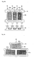
- FIGs. 5A and 5B are views illustrating barrier rib structures of discharge cell structures in a plasma display panel according to a first embodiment of the present invention.
- FIG. 5A illustrates the barrier rib structure in a stripe-type discharge cell structure according to the present invention
- FIG. 5B illustrates the barrier rib structure in a well-type discharge cell structure according to the present invention.
- the inventive plasma display panel includes a first barrier rib 31 and a second barrier rib 31' each disposed at a rear substrate.
- the first barrier rib 31 partitions red (R), green (G) and blue (B) sub-pixels 201a, 201 b and 201 c.
- the second barrier rib 31' partitions a unit pixel 201, which is constituted of the R, G, B sub-pixels 201 a, 201 b and 201 c, and an adjacent unit pixel.
- the width "a" is much greater than the width "b".
- the width "a" of the second barrier rib 31' functioning as a boundary between the unit pixel and the adjacent unit pixel is greater than the width "b" of the first barrier rib 31 functioning as a boundary between the sub-pixels.
- a black-color material layer is formed on the first barrier rib 31 and the second barrier rib 31'.
- the inventive barrier rib can be manufactured using not only a sand blasting method but also any one of a screen printing method, an additive method and a photosensitive paste method.
- the inventive barrier rib is applicable not only to the stripe-type and well-type discharge cell structures of FIGs. 5A and 5B, but also to a delta-type or honey-type discharge cell structure.
- a unit pixel color combined due to light emission of the R, G, B sub-pixels is more spaced apart from an adjacent unit pixel color, thereby improving a visual color mixture.
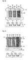
- FIGs. 6A and 6B are views illustrating barrier rib structures and black matrix structures of discharge cell structures in a plasma display panel according to a second embodiment of the present invention.
- FIG. 6A illustrates the barrier rib structure and the black matrix structure in a stripe-type discharge cell structure
- FIG. 6B illustrates the barrier rib structure and the black matrix structure in a well-type discharge cell structure.
- the inventive barrier rib structures are the same as those of the first embodiment and therefore, their descriptions are omitted.
- a black matrix having a predetermined pattern is formed at a front substrate. It is desirable that a barrier rib has a white-color material to compensate for luminance reduction caused by the black matrix of the front substrate in the PDP.
- a first black matrix 13a is formed at the front substrate to be in a vertical direction of a first barrier rib 31 and a second barrier rib 31'.
- a second black matrix 13b is formed in an extension direction of the second barrier rib 31' partitioning unit pixels.
- the second black matrix 13b is extended from the second barrier rib 31' and formed on the front substrate.
- the second barrier rib 31' has a greater width than the first barrier rib 31 partitioning sub-pixels.
- the black matrix can be formed in the extension direction of the first barrier rib 31 partitioning the sub-pixels.
- the black matrix is formed of paste in a screen-printing method and the like.
- the paste employs a metallic compound such as chrome (Cr) or a nonmetallic compound.
- Cr chrome
- a voltage is applied to a plurality of electrodes formed at the front substrate, a dielectric material covering the electrodes is broken down in dielectricity, thereby conducting the black matrix in a cell discharge. Accordingly, there is a drawback in that an erroneous cell discharge is caused in the PDP.
- FIGs. 7A and 7B are views illustrating the black matrix structures of the discharge cell structures in the plasma display panel according to the present invention.
- the black matrixes 13a and 13b are almost the same as those of FIGs. 6A and 6B.
- the second black matrix 1 3b is formed in the extension direction of the second barrier rib 31' to have a predetermined gap (d) partitioning the unit pixel 201 at its center portion.
- the black matrix is short-circuited to secure electrical insulation.
- the barrier rib structure is the same as that of the first embodiment of the present invention.
- the color mixture caused by light emission of each unit pixel can be improved and concurrently, the reflectance against external light and internal transmitted light can be decreased, thereby improving the contrast characteristic.
- FIGs. 8A and 8B are views illustrating barrier rib structures of discharge cell structures in a plasma display panel according to a third embodiment of the present invention.
- FIG. 8A illustrates the barrier rib structure of a stripe-type discharge cell structure
- FIG. 8B illustrates the barrier rib structure of a well-type discharge cell structure.
- the barrier rib structures are the same as those of the first embodiment of the present invention and therefore, their descriptions are omitted. However, the barrier rib structures are all formed of black-color material.
- the inventive PDP having the barrier rib structure color mixture caused by light emission of each unit pixel can be improved, and the barrier rib can be formed of black-color material, thereby decreasing reflectance against external light and improving a contrast characteristic.
- FIGs. 9A through 9D are views sequentially illustrating a method for manufacturing the barrier rib in the plasma display panel according to an embodiment of the present invention.
- a dielectric material 41 is formed on a lower substrate 40 having an address electrode (not shown) mounted thereon.
- a barrier rib paste 31 is formed at a predetermined thickness on the dielectric material 41.
- the barrier rib paste 31 is formed of black-color material in a printing method or a coating method so as to reduce the reflectance against the external light.
- a dry film resin (Hereinafter, referred to as "DFR") 42 is formed on the barrier rib paste 31 in a laminating process.
- a photo mask 43 is aligned on the DFR 42, and light is irradiated on the photo mask 43.
- the photo mask 43 has a pattern of irregular intervals (d1 and d2) between a light blocking unit 43a and a light transmitting unit 43b. This is to differentiate the barrier ribs in width, that is, the barrier rib functioning as the boundary between the R, G, B sub-pixels and the barrier rib functioning as the boundary between the unit pixels constituted of the R, G, B sub-pixels.
- non-exposure region a DFR 42 region not exposed to light
- exposure region a DFR 42 region exposed to light
- a sand blasting device 44 is placed and driven over the developed barrier rib paste 31 and the DFR 42 to spray sand particles onto the barrier rib paste 31.
- the barrier rib paste 31 is cut out due to sputtering of the sand particles whereas the barrier rib paste 31 corresponding to the barrier rib is protected by the DFR 42 pattern.
- the DFR 42 is peeled off in a peeling-off process.
- the barrier rib paste 31 is plasticized, thereby completing the barrier rib. As a result, a discharge space is concavely provided between the barrier ribs.
- the inventive barrier rib of the PDP manufactured through the above processes when the PDP is driven, the visual color mixture of the discharge cell is improved and concurrently, the barrier rib paste is formed of the black-color material, thereby reducing the reflectance against the external light and improving the contrast characteristic.
- FIGs. 10A through 10D are views sequentially illustrating a method for manufacturing a barrier rib in a plasma display panel according to another embodiment of the present invention.
- a dielectric material 41 is formed on a lower substrate 40 having an address electrode (not shown) mounted thereon, and then a white-color barrier rib paste 31 is formed at a predetermined thickness on the dielectric material 41.
- a photosensitive black-color paste 31 a is layered on the barrier rib paste 31 in a printing method or a coating method.
- a dry film resin (DFR) 42 is formed on the photosensitive black-color paste in a laminating process.
- a photo mask 43 is aligned on the DFR 42 and then, light is irradiated on the photo mask 43.
- the photo mask has a pattern of irregular intervals (d1 and d2) between a light blocking unit 43a and a light transmitting unit 43b. This is to differentiate the barrier ribs in width, that is, the barrier rib functioning as the boundary between the R, G, B sub-pixels and the barrier rib functioning as the boundary between the unit pixels constituted of the R, G, B sub-pixels.
- non-exposure region a DFR 42 region not exposed to light
- exposure region a DFR 42 region exposed to light
- a sand blasting device 44 is placed and driven over the developed barrier rib paste 31, the photosensitive black-color paste 31 a and the DFR 42 to spray sand particles onto the barrier rib paste 31.
- the barrier rib paste 31 is cut out due to sputtering of the sand particles whereas the barrier rib paste 31 corresponding to the barrier rib is protected by the DFR 42 pattern.
- the DFR 42 is peeled off in a peeling-off process.
- the barrier rib paste 31 is plasticized, thereby completing the barrier rib. As a result, a discharge space is concavely provided between the barrier ribs.
- the luminance characteristic is not only improved, but also the contrast characteristic is improved.
- the present invention has an effect in that the color mixture caused by the light emission of each unit discharge cell is improved in the PDP, and the reflectance against the external light and the internal light is reduced, thereby improving the contrast characteristic.
Landscapes
- Engineering & Computer Science (AREA)
- Physics & Mathematics (AREA)
- Plasma & Fusion (AREA)
- Manufacturing & Machinery (AREA)
- Gas-Filled Discharge Tubes (AREA)
Applications Claiming Priority (4)
| Application Number | Priority Date | Filing Date | Title |
|---|---|---|---|
| KR1020040021696A KR100592127B1 (ko) | 2004-03-30 | 2004-03-30 | 플라즈마 디스플레이 패널 및 그의 제조방법 |
| KR2004021700 | 2004-03-30 | ||
| KR2004021696 | 2004-03-30 | ||
| KR1020040021700A KR20050096992A (ko) | 2004-03-30 | 2004-03-30 | 플라즈마 디스플레이 패널 |
Publications (1)
| Publication Number | Publication Date |
|---|---|
| EP1596410A1 true EP1596410A1 (fr) | 2005-11-16 |
Family
ID=34934488
Family Applications (1)
| Application Number | Title | Priority Date | Filing Date |
|---|---|---|---|
| EP05006482A Withdrawn EP1596410A1 (fr) | 2004-03-30 | 2005-03-24 | Panneau d'affichage à plasma et son procédé de fabrication |
Country Status (4)
| Country | Link |
|---|---|
| US (2) | US7224120B2 (fr) |
| EP (1) | EP1596410A1 (fr) |
| JP (1) | JP2005285771A (fr) |
| CN (1) | CN1677608A (fr) |
Cited By (11)
| Publication number | Priority date | Publication date | Assignee | Title |
|---|---|---|---|---|
| EP1806763B1 (fr) * | 2006-01-05 | 2012-04-25 | Lg Electronics Inc. | Panneau d'affichage à plasma |
| US20120131116A1 (en) * | 2010-11-15 | 2012-05-24 | Van Quy Tu | Controlling data transfer on mobile devices |
| US8799227B2 (en) | 2011-11-11 | 2014-08-05 | Blackberry Limited | Presenting metadata from multiple perimeters |
| US9065771B2 (en) | 2012-10-24 | 2015-06-23 | Blackberry Limited | Managing application execution and data access on a device |
| US9075955B2 (en) | 2012-10-24 | 2015-07-07 | Blackberry Limited | Managing permission settings applied to applications |
| US9161226B2 (en) | 2011-10-17 | 2015-10-13 | Blackberry Limited | Associating services to perimeters |
| US9282099B2 (en) | 2005-06-29 | 2016-03-08 | Blackberry Limited | System and method for privilege management and revocation |
| US9369466B2 (en) | 2012-06-21 | 2016-06-14 | Blackberry Limited | Managing use of network resources |
| USRE46083E1 (en) | 2004-04-30 | 2016-07-26 | Blackberry Limited | System and method for handling data transfers |
| US9497220B2 (en) | 2011-10-17 | 2016-11-15 | Blackberry Limited | Dynamically generating perimeters |
| US10848520B2 (en) | 2011-11-10 | 2020-11-24 | Blackberry Limited | Managing access to resources |
Families Citing this family (13)
| Publication number | Priority date | Publication date | Assignee | Title |
|---|---|---|---|---|
| KR20060022200A (ko) * | 2004-09-06 | 2006-03-09 | 엘지전자 주식회사 | 플라즈마 표시 패널 |
| KR100670245B1 (ko) * | 2004-12-09 | 2007-01-16 | 삼성에스디아이 주식회사 | 플라즈마 디스플레이 패널 |
| KR20060088670A (ko) * | 2005-02-02 | 2006-08-07 | 엘지전자 주식회사 | 플라즈마 디스플레이 패널 |
| KR100667332B1 (ko) * | 2005-07-18 | 2007-01-12 | 엘지전자 주식회사 | 플라즈마 디스플레이 장치 |
| JP2007171890A (ja) * | 2005-11-22 | 2007-07-05 | Bridgestone Corp | 情報表示用パネル |
| US20090278438A1 (en) * | 2005-12-26 | 2009-11-12 | Minoru Hasegawa | Plasma display panel |
| JP4360370B2 (ja) * | 2005-12-27 | 2009-11-11 | パナソニック株式会社 | プラズマディスプレイパネル |
| KR100814828B1 (ko) * | 2006-10-11 | 2008-03-20 | 삼성에스디아이 주식회사 | 플라즈마 디스플레이 패널 |
| KR20080069863A (ko) * | 2007-01-24 | 2008-07-29 | 삼성에스디아이 주식회사 | 플라즈마 디스플레이 패널 |
| EP2122409B1 (fr) * | 2007-02-25 | 2016-12-07 | Humaneyes Technologies Ltd. | Procédé et système pour étalonner et/ou visualiser un dispositif d'affichage de plusieurs images et pour réduire les artefacts fantômes |
| WO2009013744A2 (fr) * | 2007-07-23 | 2009-01-29 | Humaneyes Technologies Ltd. | Dddispositifs d'affichage à vues multiples et leurs procédés de fabrication |
| US9614191B2 (en) | 2013-01-17 | 2017-04-04 | Kateeva, Inc. | High resolution organic light-emitting diode devices, displays, and related methods |
| US9444050B2 (en) | 2013-01-17 | 2016-09-13 | Kateeva, Inc. | High resolution organic light-emitting diode devices, displays, and related method |
Citations (5)
| Publication number | Priority date | Publication date | Assignee | Title |
|---|---|---|---|---|
| US5541479A (en) * | 1993-09-13 | 1996-07-30 | Pioneer Electronic Corporation | Plasma display device |
| EP1119015A1 (fr) * | 1998-09-29 | 2001-07-25 | Fujitsu Limited | Procede de fabrication d'un ecran a plasma et d'une structure de substrat |
| EP1187166A2 (fr) * | 2000-09-06 | 2002-03-13 | Fujitsu Hitachi Plasma Display Limited | Panneau d'affichage à plasma et son procédé de fabrication |
| US20020101151A1 (en) * | 2000-12-05 | 2002-08-01 | Choi Do-Hyun | Plasma switched organic photoluminescent display |
| US6611099B1 (en) * | 1998-03-31 | 2003-08-26 | Kabushiki Kaisha Toshiba | Plasma display panel using Xe discharge gas |
Family Cites Families (12)
| Publication number | Priority date | Publication date | Assignee | Title |
|---|---|---|---|---|
| JPH05258682A (ja) | 1992-03-16 | 1993-10-08 | Hitachi Ltd | 陰極線管電子銃およびその製造方法 |
| JP2000040472A (ja) * | 1998-05-21 | 2000-02-08 | Toray Ind Inc | プラズマディスプレイ用部材およびその製造方法ならびにプラズマディスプレイ |
| JP2000113825A (ja) * | 1998-10-05 | 2000-04-21 | Matsushita Electric Ind Co Ltd | プラズマディスプレイパネル |
| JP3860673B2 (ja) * | 1999-02-18 | 2006-12-20 | 京セラ株式会社 | プラズマディスプレイパネルおよびその製造方法 |
| KR100577161B1 (ko) | 1999-06-24 | 2006-05-09 | 엘지전자 주식회사 | 플라즈마 디스플레이 패널 |
| CN1129106C (zh) | 2000-01-18 | 2003-11-26 | 友达光电股份有限公司 | 等离子显示器的背面基板与其制作方法 |
| JP4069583B2 (ja) * | 2000-03-28 | 2008-04-02 | 三菱電機株式会社 | プラズマディスプレイ装置 |
| JP2003068212A (ja) * | 2001-08-28 | 2003-03-07 | Fujitsu Ltd | プラズマディスプレイパネル |
| JP2003168373A (ja) * | 2001-11-29 | 2003-06-13 | Mitsubishi Electric Corp | 面放電ac型プラズマディスプレイパネル用前面基板、面放電ac型プラズマディスプレイパネル及び面放電ac型プラズマディスプレイ装置 |
| TWI247325B (en) * | 2003-06-27 | 2006-01-11 | Chunghwa Picture Tubes Ltd | Barrier rib structure for plasma display panel |
| TWI222657B (en) * | 2003-08-27 | 2004-10-21 | Au Optronics Corp | Plasma display panel |
| KR20060088670A (ko) * | 2005-02-02 | 2006-08-07 | 엘지전자 주식회사 | 플라즈마 디스플레이 패널 |
-
2005
- 2005-03-24 EP EP05006482A patent/EP1596410A1/fr not_active Withdrawn
- 2005-03-28 US US11/092,735 patent/US7224120B2/en not_active Expired - Fee Related
- 2005-03-29 JP JP2005095195A patent/JP2005285771A/ja active Pending
- 2005-03-30 CN CN200510058862.0A patent/CN1677608A/zh active Pending
-
2007
- 2007-03-23 US US11/690,447 patent/US7663316B2/en not_active Expired - Fee Related
Patent Citations (5)
| Publication number | Priority date | Publication date | Assignee | Title |
|---|---|---|---|---|
| US5541479A (en) * | 1993-09-13 | 1996-07-30 | Pioneer Electronic Corporation | Plasma display device |
| US6611099B1 (en) * | 1998-03-31 | 2003-08-26 | Kabushiki Kaisha Toshiba | Plasma display panel using Xe discharge gas |
| EP1119015A1 (fr) * | 1998-09-29 | 2001-07-25 | Fujitsu Limited | Procede de fabrication d'un ecran a plasma et d'une structure de substrat |
| EP1187166A2 (fr) * | 2000-09-06 | 2002-03-13 | Fujitsu Hitachi Plasma Display Limited | Panneau d'affichage à plasma et son procédé de fabrication |
| US20020101151A1 (en) * | 2000-12-05 | 2002-08-01 | Choi Do-Hyun | Plasma switched organic photoluminescent display |
Cited By (19)
| Publication number | Priority date | Publication date | Assignee | Title |
|---|---|---|---|---|
| USRE46083E1 (en) | 2004-04-30 | 2016-07-26 | Blackberry Limited | System and method for handling data transfers |
| USRE49721E1 (en) | 2004-04-30 | 2023-11-07 | Blackberry Limited | System and method for handling data transfers |
| USRE48679E1 (en) | 2004-04-30 | 2021-08-10 | Blackberry Limited | System and method for handling data transfers |
| US9734308B2 (en) | 2005-06-29 | 2017-08-15 | Blackberry Limited | Privilege management and revocation |
| US9282099B2 (en) | 2005-06-29 | 2016-03-08 | Blackberry Limited | System and method for privilege management and revocation |
| US10515195B2 (en) | 2005-06-29 | 2019-12-24 | Blackberry Limited | Privilege management and revocation |
| EP1806763B1 (fr) * | 2006-01-05 | 2012-04-25 | Lg Electronics Inc. | Panneau d'affichage à plasma |
| US20120131116A1 (en) * | 2010-11-15 | 2012-05-24 | Van Quy Tu | Controlling data transfer on mobile devices |
| US9497220B2 (en) | 2011-10-17 | 2016-11-15 | Blackberry Limited | Dynamically generating perimeters |
| US9402184B2 (en) | 2011-10-17 | 2016-07-26 | Blackberry Limited | Associating services to perimeters |
| US10735964B2 (en) | 2011-10-17 | 2020-08-04 | Blackberry Limited | Associating services to perimeters |
| US9161226B2 (en) | 2011-10-17 | 2015-10-13 | Blackberry Limited | Associating services to perimeters |
| US10848520B2 (en) | 2011-11-10 | 2020-11-24 | Blackberry Limited | Managing access to resources |
| US9720915B2 (en) | 2011-11-11 | 2017-08-01 | Blackberry Limited | Presenting metadata from multiple perimeters |
| US8799227B2 (en) | 2011-11-11 | 2014-08-05 | Blackberry Limited | Presenting metadata from multiple perimeters |
| US9369466B2 (en) | 2012-06-21 | 2016-06-14 | Blackberry Limited | Managing use of network resources |
| US11032283B2 (en) | 2012-06-21 | 2021-06-08 | Blackberry Limited | Managing use of network resources |
| US9075955B2 (en) | 2012-10-24 | 2015-07-07 | Blackberry Limited | Managing permission settings applied to applications |
| US9065771B2 (en) | 2012-10-24 | 2015-06-23 | Blackberry Limited | Managing application execution and data access on a device |
Also Published As
| Publication number | Publication date |
|---|---|
| JP2005285771A (ja) | 2005-10-13 |
| US7663316B2 (en) | 2010-02-16 |
| US20070159102A1 (en) | 2007-07-12 |
| US20050218807A1 (en) | 2005-10-06 |
| US7224120B2 (en) | 2007-05-29 |
| CN1677608A (zh) | 2005-10-05 |
Similar Documents
| Publication | Publication Date | Title |
|---|---|---|
| US7663316B2 (en) | Plasma display panel having barrier ribs with black matrix | |
| US6965200B2 (en) | Plasma display device having barrier ribs | |
| JP2005285771A5 (fr) | ||
| JP2004312012A (ja) | フラットパネルディスプレイ装置の電磁波遮蔽膜及びこれを含む前面フィルタ。 | |
| JP3476217B2 (ja) | プラズマディスプレイパネル | |
| JP3501498B2 (ja) | プラズマディスプレイパネル | |
| US8410694B2 (en) | Plasma display panel | |
| US20090058298A1 (en) | Plasma display panel and method of fabricating the same | |
| US20090315460A2 (en) | Plasma display panel | |
| US20060175949A1 (en) | Plasma display panel and manufacturing method thereof | |
| EP1632977B1 (fr) | Panneau d'affichage à plasma | |
| EP1696456B1 (fr) | Appareil d'affichage à plasma | |
| KR100592127B1 (ko) | 플라즈마 디스플레이 패널 및 그의 제조방법 | |
| KR100777729B1 (ko) | 플라즈마 디스플레이 패널 | |
| KR100592249B1 (ko) | 플라즈마 디스플레이 패널의 하판 | |
| US7405517B2 (en) | Plasma display panel | |
| JP2008084647A (ja) | プラズマディスプレイパネル | |
| JP2003229063A (ja) | プラズマ表示装置 | |
| JP2004335340A (ja) | プラズマディスプレイパネル、その製造方法、およびその製造装置 | |
| JP2007134264A (ja) | プラズマディスプレイパネル | |
| JP2005222702A (ja) | 交流駆動型プラズマ表示装置及びそのアドレス・表示分離駆動方式 | |
| JP2013222572A (ja) | プラズマディスプレイパネル | |
| KR20060122020A (ko) | 플라즈마 디스플레이 패널 및 그 제조방법 | |
| KR20060029094A (ko) | 플라즈마 디스플레이 패널 | |
| KR20070097191A (ko) | 플라즈마 디스플레이 패널 |
Legal Events
| Date | Code | Title | Description |
|---|---|---|---|
| PUAI | Public reference made under article 153(3) epc to a published international application that has entered the european phase |
Free format text: ORIGINAL CODE: 0009012 |
|
| AK | Designated contracting states |
Kind code of ref document: A1 Designated state(s): AT BE BG CH CY CZ DE DK EE ES FI FR GB GR HU IE IS IT LI LT LU MC NL PL PT RO SE SI SK TR |
|
| AX | Request for extension of the european patent |
Extension state: AL BA HR LV MK YU |
|
| 17P | Request for examination filed |
Effective date: 20060315 |
|
| AKX | Designation fees paid |
Designated state(s): DE FR GB NL |
|
| 17Q | First examination report despatched |
Effective date: 20061214 |
|
| STAA | Information on the status of an ep patent application or granted ep patent |
Free format text: STATUS: THE APPLICATION IS DEEMED TO BE WITHDRAWN |
|
| 18D | Application deemed to be withdrawn |
Effective date: 20100310 |