EP1596424B1 - Appareil d'exposition et méthode d'exposition d'un motif - Google Patents
Appareil d'exposition et méthode d'exposition d'un motif Download PDFInfo
- Publication number
- EP1596424B1 EP1596424B1 EP04711441.8A EP04711441A EP1596424B1 EP 1596424 B1 EP1596424 B1 EP 1596424B1 EP 04711441 A EP04711441 A EP 04711441A EP 1596424 B1 EP1596424 B1 EP 1596424B1
- Authority
- EP
- European Patent Office
- Prior art keywords
- silica glass
- synthetic silica
- exposure apparatus
- energy density
- light
- Prior art date
- Legal status (The legal status is an assumption and is not a legal conclusion. Google has not performed a legal analysis and makes no representation as to the accuracy of the status listed.)
- Expired - Lifetime
Links
- 238000000034 method Methods 0.000 title claims description 7
- VYPSYNLAJGMNEJ-UHFFFAOYSA-N Silicium dioxide Chemical compound O=[Si]=O VYPSYNLAJGMNEJ-UHFFFAOYSA-N 0.000 claims description 104
- 230000003287 optical effect Effects 0.000 claims description 87
- 230000014509 gene expression Effects 0.000 claims description 19
- 239000013078 crystal Substances 0.000 claims description 15
- 229910052731 fluorine Inorganic materials 0.000 claims description 13
- 239000011737 fluorine Substances 0.000 claims description 13
- 206010040925 Skin striae Diseases 0.000 claims description 11
- 239000000463 material Substances 0.000 claims description 9
- 239000000126 substance Substances 0.000 claims description 9
- 239000010453 quartz Substances 0.000 claims description 5
- 239000000758 substrate Substances 0.000 claims description 5
- 239000005304 optical glass Substances 0.000 claims description 4
- 238000011156 evaluation Methods 0.000 claims description 3
- ORUIBWPALBXDOA-UHFFFAOYSA-L magnesium fluoride Chemical compound [F-].[F-].[Mg+2] ORUIBWPALBXDOA-UHFFFAOYSA-L 0.000 claims description 2
- 229910001635 magnesium fluoride Inorganic materials 0.000 claims description 2
- TWNQGVIAIRXVLR-UHFFFAOYSA-N oxo(oxoalumanyloxy)alumane Chemical compound O=[Al]O[Al]=O TWNQGVIAIRXVLR-UHFFFAOYSA-N 0.000 claims description 2
- PXGOKWXKJXAPGV-UHFFFAOYSA-N Fluorine Chemical compound FF PXGOKWXKJXAPGV-UHFFFAOYSA-N 0.000 claims 2
- 235000012431 wafers Nutrition 0.000 description 15
- YCKRFDGAMUMZLT-UHFFFAOYSA-N Fluorine atom Chemical compound [F] YCKRFDGAMUMZLT-UHFFFAOYSA-N 0.000 description 11
- 238000005056 compaction Methods 0.000 description 9
- 230000006378 damage Effects 0.000 description 9
- 238000002474 experimental method Methods 0.000 description 8
- 238000002834 transmittance Methods 0.000 description 8
- WUKWITHWXAAZEY-UHFFFAOYSA-L calcium difluoride Chemical compound [F-].[F-].[Ca+2] WUKWITHWXAAZEY-UHFFFAOYSA-L 0.000 description 5
- 229910001634 calcium fluoride Inorganic materials 0.000 description 5
- 239000002178 crystalline material Substances 0.000 description 5
- 238000010586 diagram Methods 0.000 description 5
- 230000002349 favourable effect Effects 0.000 description 5
- 125000002887 hydroxy group Chemical group [H]O* 0.000 description 5
- 238000007654 immersion Methods 0.000 description 5
- 238000005498 polishing Methods 0.000 description 5
- UFHFLCQGNIYNRP-UHFFFAOYSA-N Hydrogen Chemical compound [H][H] UFHFLCQGNIYNRP-UHFFFAOYSA-N 0.000 description 4
- 238000005520 cutting process Methods 0.000 description 4
- 239000001257 hydrogen Substances 0.000 description 4
- 229910052739 hydrogen Inorganic materials 0.000 description 4
- 238000007493 shaping process Methods 0.000 description 4
- 239000010409 thin film Substances 0.000 description 4
- 238000011179 visual inspection Methods 0.000 description 3
- IJGRMHOSHXDMSA-UHFFFAOYSA-N Atomic nitrogen Chemical compound N#N IJGRMHOSHXDMSA-UHFFFAOYSA-N 0.000 description 2
- ZAMOUSCENKQFHK-UHFFFAOYSA-N Chlorine atom Chemical compound [Cl] ZAMOUSCENKQFHK-UHFFFAOYSA-N 0.000 description 2
- XAGFODPZIPBFFR-UHFFFAOYSA-N aluminium Chemical compound [Al] XAGFODPZIPBFFR-UHFFFAOYSA-N 0.000 description 2
- 229910052782 aluminium Inorganic materials 0.000 description 2
- 239000000460 chlorine Substances 0.000 description 2
- 229910052801 chlorine Inorganic materials 0.000 description 2
- 230000001419 dependent effect Effects 0.000 description 2
- 238000001152 differential interference contrast microscopy Methods 0.000 description 2
- 229910001873 dinitrogen Inorganic materials 0.000 description 2
- 238000009826 distribution Methods 0.000 description 2
- 230000000694 effects Effects 0.000 description 2
- 239000011521 glass Substances 0.000 description 2
- 238000011835 investigation Methods 0.000 description 2
- 230000001678 irradiating effect Effects 0.000 description 2
- 239000007788 liquid Substances 0.000 description 2
- 239000004973 liquid crystal related substance Substances 0.000 description 2
- 238000001459 lithography Methods 0.000 description 2
- 238000004519 manufacturing process Methods 0.000 description 2
- 230000002093 peripheral effect Effects 0.000 description 2
- 230000002265 prevention Effects 0.000 description 2
- 239000004065 semiconductor Substances 0.000 description 2
- 239000000377 silicon dioxide Substances 0.000 description 2
- 238000012546 transfer Methods 0.000 description 2
- XUIMIQQOPSSXEZ-UHFFFAOYSA-N Silicon Chemical compound [Si] XUIMIQQOPSSXEZ-UHFFFAOYSA-N 0.000 description 1
- 238000009825 accumulation Methods 0.000 description 1
- 230000008033 biological extinction Effects 0.000 description 1
- 230000015572 biosynthetic process Effects 0.000 description 1
- 239000000919 ceramic Substances 0.000 description 1
- 238000011109 contamination Methods 0.000 description 1
- 230000007423 decrease Effects 0.000 description 1
- 230000007547 defect Effects 0.000 description 1
- 238000005516 engineering process Methods 0.000 description 1
- 230000001771 impaired effect Effects 0.000 description 1
- 230000010354 integration Effects 0.000 description 1
- 238000005259 measurement Methods 0.000 description 1
- 230000005499 meniscus Effects 0.000 description 1
- 239000000203 mixture Substances 0.000 description 1
- 238000000206 photolithography Methods 0.000 description 1
- 230000000704 physical effect Effects 0.000 description 1
- 238000012545 processing Methods 0.000 description 1
- 230000005855 radiation Effects 0.000 description 1
- 229910052710 silicon Inorganic materials 0.000 description 1
- 239000010703 silicon Substances 0.000 description 1
Images


Classifications
-
- G—PHYSICS
- G03—PHOTOGRAPHY; CINEMATOGRAPHY; ANALOGOUS TECHNIQUES USING WAVES OTHER THAN OPTICAL WAVES; ELECTROGRAPHY; HOLOGRAPHY
- G03F—PHOTOMECHANICAL PRODUCTION OF TEXTURED OR PATTERNED SURFACES, e.g. FOR PRINTING, FOR PROCESSING OF SEMICONDUCTOR DEVICES; MATERIALS THEREFOR; ORIGINALS THEREFOR; APPARATUS SPECIALLY ADAPTED THEREFOR
- G03F7/00—Photomechanical, e.g. photolithographic, production of textured or patterned surfaces, e.g. printing surfaces; Materials therefor, e.g. comprising photoresists; Apparatus specially adapted therefor
- G03F7/70—Microphotolithographic exposure; Apparatus therefor
- G03F7/708—Construction of apparatus, e.g. environment aspects, hygiene aspects or materials
- G03F7/7095—Materials, e.g. materials for housing, stage or other support having particular properties, e.g. weight, strength, conductivity, thermal expansion coefficient
- G03F7/70958—Optical materials or coatings, e.g. with particular transmittance, reflectance or anti-reflection properties
-
- G—PHYSICS
- G03—PHOTOGRAPHY; CINEMATOGRAPHY; ANALOGOUS TECHNIQUES USING WAVES OTHER THAN OPTICAL WAVES; ELECTROGRAPHY; HOLOGRAPHY
- G03F—PHOTOMECHANICAL PRODUCTION OF TEXTURED OR PATTERNED SURFACES, e.g. FOR PRINTING, FOR PROCESSING OF SEMICONDUCTOR DEVICES; MATERIALS THEREFOR; ORIGINALS THEREFOR; APPARATUS SPECIALLY ADAPTED THEREFOR
- G03F7/00—Photomechanical, e.g. photolithographic, production of textured or patterned surfaces, e.g. printing surfaces; Materials therefor, e.g. comprising photoresists; Apparatus specially adapted therefor
- G03F7/70—Microphotolithographic exposure; Apparatus therefor
- G03F7/70008—Production of exposure light, i.e. light sources
- G03F7/70041—Production of exposure light, i.e. light sources by pulsed sources, e.g. multiplexing, pulse duration, interval control or intensity control
-
- G—PHYSICS
- G03—PHOTOGRAPHY; CINEMATOGRAPHY; ANALOGOUS TECHNIQUES USING WAVES OTHER THAN OPTICAL WAVES; ELECTROGRAPHY; HOLOGRAPHY
- G03F—PHOTOMECHANICAL PRODUCTION OF TEXTURED OR PATTERNED SURFACES, e.g. FOR PRINTING, FOR PROCESSING OF SEMICONDUCTOR DEVICES; MATERIALS THEREFOR; ORIGINALS THEREFOR; APPARATUS SPECIALLY ADAPTED THEREFOR
- G03F7/00—Photomechanical, e.g. photolithographic, production of textured or patterned surfaces, e.g. printing surfaces; Materials therefor, e.g. comprising photoresists; Apparatus specially adapted therefor
- G03F7/70—Microphotolithographic exposure; Apparatus therefor
- G03F7/70483—Information management; Active and passive control; Testing; Wafer monitoring, e.g. pattern monitoring
- G03F7/70591—Testing optical components
-
- G—PHYSICS
- G03—PHOTOGRAPHY; CINEMATOGRAPHY; ANALOGOUS TECHNIQUES USING WAVES OTHER THAN OPTICAL WAVES; ELECTROGRAPHY; HOLOGRAPHY
- G03F—PHOTOMECHANICAL PRODUCTION OF TEXTURED OR PATTERNED SURFACES, e.g. FOR PRINTING, FOR PROCESSING OF SEMICONDUCTOR DEVICES; MATERIALS THEREFOR; ORIGINALS THEREFOR; APPARATUS SPECIALLY ADAPTED THEREFOR
- G03F7/00—Photomechanical, e.g. photolithographic, production of textured or patterned surfaces, e.g. printing surfaces; Materials therefor, e.g. comprising photoresists; Apparatus specially adapted therefor
- G03F7/70—Microphotolithographic exposure; Apparatus therefor
- G03F7/708—Construction of apparatus, e.g. environment aspects, hygiene aspects or materials
- G03F7/70858—Environment aspects, e.g. pressure of beam-path gas, temperature
- G03F7/70883—Environment aspects, e.g. pressure of beam-path gas, temperature of optical system
-
- G—PHYSICS
- G03—PHOTOGRAPHY; CINEMATOGRAPHY; ANALOGOUS TECHNIQUES USING WAVES OTHER THAN OPTICAL WAVES; ELECTROGRAPHY; HOLOGRAPHY
- G03F—PHOTOMECHANICAL PRODUCTION OF TEXTURED OR PATTERNED SURFACES, e.g. FOR PRINTING, FOR PROCESSING OF SEMICONDUCTOR DEVICES; MATERIALS THEREFOR; ORIGINALS THEREFOR; APPARATUS SPECIALLY ADAPTED THEREFOR
- G03F7/00—Photomechanical, e.g. photolithographic, production of textured or patterned surfaces, e.g. printing surfaces; Materials therefor, e.g. comprising photoresists; Apparatus specially adapted therefor
- G03F7/70—Microphotolithographic exposure; Apparatus therefor
- G03F7/708—Construction of apparatus, e.g. environment aspects, hygiene aspects or materials
- G03F7/70908—Hygiene, e.g. preventing apparatus pollution, mitigating effect of pollution or removing pollutants from apparatus
- G03F7/70941—Stray fields and charges, e.g. stray light, scattered light, flare, transmission loss
Definitions
- the present invention relates to an exposure apparatus and a method of exposing a pattern using the exposure apparatus.
- US 2002/0135746 A1 discloses an optical system provided in a projection exposure apparatus for processing an excimer laser beam.
- the optical system includes at least one optical member made of silica glass having a chlorine concentration of about 1 ppm or less, and at least one optical member made of silica glass having a chlorine concentration of about 1 ppm to about 200 ppm.
- EP 1 154 330 A discloses an exposure apparatus which transfers an image of a pattern on a reticle onto a wafer by synchronously scanning the reticle and the wafer with respect to a projection optical system in a state in which the reticle is illuminated with an exposure light beam from an exposure light source subjected to pulse light emission via a fly's eye lens, a movable blind, a main condenser lens system, and a fixed blind.
- First and second uneven illuminance-correcting plates, on which shielding line groups for correcting convex and concave uneven illuminance are depicted, are arranged at a position defocused from a conjugate plane with respect to a pattern plane of the reticle.
- a third correcting plate for roughly correcting uneven illuminance is arranged at a position further defocused therefrom. It is possible to enhance the uniformity of the totalized exposure amount on the wafer or the telecentricity when the exposure is performed in accordance with the scanning exposure system.
- EP-A2-1103528 discloses a UV lithography apparatus operating with radiations from 155 to 195 nm in wavelength, and using silica glass optical material that suffers less damage caused by the high power output of UV laser light sources.
- the material has ultrahigh purity, and contains from 1 to 10 wtppm of OH groups, from 100 to 10,000 wtppm of F, and from 1 x 10 17 to 1 x 10 19 molecules/cm 3 of H 2 .
- a reduction projection aligner or a photolithography apparatus is mainly used.
- a wide exposure area and a high resolution over the entire exposure area are required for a projection optical system used in such an apparatus.
- NA numerical aperture
- KrF (248 nm) excimer lasers are mainly used as light sources of exposure apparatuses.
- ArF excimer lasers which are deep ultraviolet rays having shorter wavelength, have been developed.
- the first type is a reduction in internal transmittance caused by the generation of internal defects (see Japanese Patent Application Laid-Open Gazette No. Hei 8-259255 ).
- the second type is a refractive index change associated with a volume change such as compaction or expansion (see International Application National-Phase Publication No. 2000-517284 ).
- the third type is a surface state change such as the destruction or contamination of an optical thin film (see Japanese Patent Application Laid-Open Gazette Nos. 2002-14202 and Hei 11-52102 ).
- This microchannel phenomenon occurs due to extremely long continuous irradiation homogeneous at low energy densities in a practical range under normal use conditions of an exposure apparatus. Accordingly, it is necessary to take prevention measures against mechanical damage resulting from this phenomenon.
- an object of the present invention is to provide an exposure apparatus in which the generation of microchannels can be reduced.
- the present inventors investigated generation conditions by actually generating microchannels by applying KrF or ArF excimer laser light, which is pulsed light, to each of various kinds of optical components made of synthetic silica glass, a quartz single crystal, a calcium fluoride single crystal, and the like.
- the cause of the generation of microchannels is self-focusing resulting from a refractive index change, which is a characteristic phenomenon of synthetic silica. That is, when synthetic silica glass is irradiated with the laser light, a refractive index change accompanied by compaction occurs. While this irradiation is repeated, a small amount of a refractive index change is accumulated to remain as a greatly-varied refractive index distribution in the optical component. Thus, light is bent toward a portion having a higher refractive index, and the irradiation light is gradually self-focused near the back face of the optical component. Then, at last, the energy density of the irradiation light becomes as high as it exceeds the destruction threshold of the optical component near the back face.
- Fig. 1 is a graph showing the relationship between the energy density I per pulse and the number N of pulses necessary for the generation of microchannels in the irradiation of a synthetic silica glass sample with excimer laser light.
- the sample used in the irradiation experiment was prepared by cutting synthetic silica glass containing 1100 ppm OH groups and 2 ⁇ 10 18 hydrogen molecules/cm 3 to a size having a diameter of 30 mm and a thickness of 10 mm, and by optically polishing both faces having diameters of 30 mm.
- KrF excimer laser light or ArF excimer laser light which is limited by an aperture and which has a diameter of 5 mm was directly applied to the sample from a light source without being passed through an optical component such as a lens or a homogenizer.
- the energy density per pulse of the laser light was adjusted by changing the discharge voltage, and the value was measured by placing a Joule meter at the position of the sample.
- the sample was placed inside a box made of aluminum, and the atmosphere in the box was replaced with dry nitrogen gas.
- the energy density of the laser light was fixed, and predetermined pulses of the laser light were applied.
- the pulse width ⁇ of the laser light is 20 ns in both the cases of KrF and ArF excimer lasers.
- the presence or absence of microchannels was confirmed by visual inspection by irradiating the sample with the light of a condenser lamp.
- the straight line K 10 indicates a correlation relating to KrF excimer laser light
- the straight line A 10 indicates a correlation relating to ArF excimer laser light.
- microchannels are more prone to be generated as the energy density I per pulse of applied pulsed light increases. Further, it was revealed that the number N of pulses necessary for the generation of microchannels has a correlation with the energy density I per pulse and varies in inverse proportion to I squared.
- microchannels relate to a refractive index change ⁇ n of synthetic silica glass.
- microchannels were generated when ⁇ n is 20 ppm in the case of KrF excimer laser light, and when ⁇ n is 2 ppm in the case of ArF excimer laser light.
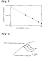
- a plurality of cuboids having 15 mm by 15 mm squares and thicknesses changed in the range of 30 mm to 100 mm were cut out from synthetic silica glass containing 1100 ppm OH groups and 2 ⁇ 10 18 hydrogen molecules/cm 3 , and formed into samples by optically polishing both faces which are 15 mm by 15 mm squares. These samples were irradiated with ArF excimer laser light having an energy density of 20 mJ ⁇ cm -2 ⁇ pulse -1 , and thresholds at which microchannels are generated were found. The result is shown in Fig. 2 .
- a relational expression for specifying a favorable range of the thickness of an optical component of the exposure apparatus can be derived by substituting 10 10 pulses to N of any one of the above-described relational expressions.
- 10 10 pulses of pulsed light can be applied without generating microchannels if the following is satisfied: ⁇ ⁇ ⁇ 2 L ⁇ 1.7 ⁇ 0.02 ns ⁇ m J ⁇ 2 ⁇ c m 2.3 pulse 2
- 10 10 pulses of pulsed light can be applied without generating microchannels if the following is satisfied: ⁇ ⁇ ⁇ 2 L ⁇ 1.7 ⁇ 25 ns ⁇ m J ⁇ 2 ⁇ c m 2.3 pulse 2
- the present invention provides an exposure apparatus as defined in claim 1 and an exposure apparatus as defined in claim 2.
- the present inventors subsequently studied the correlation between the microchannel phenomenon and the composition and various physical properties of an optical component, and come to make the preferred embodiments of the invention described in dependent claims 3, 4, 7 and 8 as means for reducing the generation of microchannels.
- the present inventors also studied the relationship between the beam quality of pulsed light and microchannels and obtained the following knowledge.
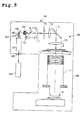
- Fig. 3 shows a schematic diagram of a differential interference contrast microscopy image of microchannels in a back face of a sample.
- the symbols * represent microchannels
- the signs m denote three grooves linearly extending.
- the grooves m were formed approximately parallel to each other, and the intervals therebetween were approximately 0.1 mm.
- microchannels are generated in the vicinity of the boundary between an irradiated portion and a non-irradiated portion and along the grooves m having intervals of approximately 0.1 mm.
- the grooves m having intervals of 0.1 mm in the back face of the sample are structures based on the energy density inhomogeneity which excimer laser light has. From the fact that microchannels are generated along these grooves m, the following can be speculated; the probability was indicated that the generation of microchannels is accelerated because, as shown in Fig. 3 , there are extremely fine and sharp structures of energy density inhomogeneity.
- places where microchannels are generated are places where the energy density is high.
- a method of exposing a pattern is defined in claim 9.
- the thickness of the at least one synthetic silica glass component, and the pulse width and the energy density per pulse of the pulsed light applied to the at least one synthetic silica glass component are defined as a specific function. Accordingly, the generation of microchannels at the time of ultraviolet light irradiation can be reduced in the face of the at least one synthetic silica glass component which is closer to an exposure object. This can prevent mechanical damage of the at least one synthetic silica glass component when the exposure object is exposed to light, and can improve the life of the exposure apparatus.
- the number of synthetic silica glass components is half or more of the total number of synthetic silica glass components. Accordingly, the life of the exposure apparatus can be further improved.
- a plurality of optical components to which ultraviolet light having an energy density of a predetermined quantity or more is applied are formed of a single crystal or anhydrous silica glass doped with fluorine, with which the generation of microchannels can be reduced. Accordingly, the generation of microchannels can be reduced, and the life of the exposure apparatus can be improved.
- a plurality of optical components to which ultraviolet light having an energy density of a predetermined quantity or more is applied are formed of the anhydrous silica glass doped with fluorine in which the amount of a refractive index change measured at a wavelength of 633 nm is 3 ppm or less after the application of 1 ⁇ 10 7 pulses of ArF excimer laser light having an energy density of 30 mJ ⁇ cm -2 ⁇ pulse -1 . Accordingly, the generation of microchannels can be reduced, and the life of the exposure apparatus can be improved.
- optical components placed closer to the light source compared to the at least one synthetic silica glass component are classified into any one of striae grades 1 to 3 in an evaluation according to Japanese Optical Glass Industrial Standards (JOGIS) 11-1975. Accordingly, the energy density inhomogeneity of light, which becomes a cause of the generation of microchannels, is not generated by striae of the at least one synthetic silica glass component when pulsed light passes through the at least one synthetic silica glass component. Consequently, pulsed light containing energy density inhomogeneity is not applied to optical components placed closer to the exposure object than the at least one synthetic silica glass component is. Thus, the generation of microchannels can be reduced, and the life of the exposure apparatus can be further improved.
- JGIS Japanese Optical Glass Industrial Standards
- the sizes of foreign substances and bubbles contained in optical components placed closer to the light source than the at least one synthetic silica glass component are 1 ⁇ m or less. Accordingly, the energy density inhomogeneity of light, which becomes a cause of the generation of microchannels, is not generated when pulsed light passes. Thus, the generation of microchannels can be reduced, and the life of the exposure apparatus can be improved.
- the energy density inhomogeneity of pulsed light is reduced to a predetermined range. Accordingly, there is no slight and greatly-varied energy density inhomogeneity which is prone to become a cause of the generation of microchannels. Thus, the generation of microchannels can be reduced, and the life of the exposure apparatus can be improved.
- none of the at least one synthetic silica glass component is placed in the space between the light source and the homogenizer placed closest to the light source. Accordingly, ultraviolet light in which energy density inhomogeneity that becomes a cause of the generation of microchannels is reduced can be applied to the at least one synthetic silica glass component. Thus, the generation of microchannels can be reduced, and the life of the exposure apparatus can be improved.
- any one of the exposure apparatuses of the present invention in which the generation of microchannels is reduced is used. Accordingly, stable exposure characteristics can be maintained for a long period of time.
- Fig. 4 is an exposure apparatus according to a favorable embodiment of the present invention.
- This exposure apparatus is constituted so that ultraviolet light which has a wavelength of 300 nm or less and which is applied from a light source 1 is converted into a parallel beam in a beam-shaping optical system 3 having a plurality of lenses 2 placed therein, applied to a mask 11 through an integrator 7 such as a fly's-eye lens and a condenser lens 9 after the deviation and the like of the beam is corrected in a homogenizer 5 including a diffraction grating 4a and a lens 4b to reduce energy density inhomogeneity, and then passed through a projection optical system 13 including a large number of lenses 12; and that an exposure shape such as a circuit pattern of the mask 11 is transferred onto an exposure object 15 such as a wafer.
- pulsed light having a wavelength of 300 nm or less such as KrF excimer laser light, or pulsed light having a wavelength of 200 nm or less, such as ArF excimer laser light
- the integrator 7 such as a fly's-eye lens acts as a homogenizer even by itself alone.
- synthetic silica glass components formed from synthetic silica glass are used as some or all of a large number of optical components such as the lenses 2, 4b, 7, 9, and 12 and the diffraction grating 4a.
- the generation of microchannels in such synthetic silica glass components is reduced.
- a synthetic silica glass component so that the thickness of the synthetic silica glass component, the energy density per pulse of pulsed light applied to the synthetic silica glass component, and the pulse width of the pulsed light satisfy the following expression (1).
- the synthetic silica glass component in an exposure apparatus which applies pulsed light having a wavelength of 200 nm or less, it is particularly preferable to form the synthetic silica glass component so that the relationship of the following expression (2) is satisfied.
- L is the thickness (unit: cm) of the synthetic silica glass component
- I is the energy density (unit: mJ ⁇ cm -2 ⁇ pulse -1 ) per pulse of the pulsed light applied to the synthetic silica glass component
- ⁇ is the pulse width (unit: ns) of the pulsed light.
- the thickness of the synthetic silica glass component is the thickness measured along the optical axis of the synthetic silica glass component.
- the thickness is a center thickness.
- the thickness is the distance between the outer peripheral portions.
- the thickness is a value obtained by measuring the distance between the center of the convex face and the outer peripheral portion of the concave face along the optical axis.
- the present invention does not require that all synthetic silica glass components constituting the exposure apparatus satisfy the aforementioned relational expressions.
- a component such as a lens 2 directly behind the light source, into which light rays having an extremely high energy density enter, if an attempt to prevent microchannels is made by applying the aforementioned relational expressions, the thickness L of the component becomes extremely small and is practically difficult to realize that microchannels are prevented.
- the proportion of relevant components to the entire optical system is very small.
- the number of synthetic silica glass components satisfying the relationship of the aforementioned expression (1) is half or more of the total number of synthetic silica glass components constituting the exposure apparatus.
- the number of synthetic silica glass components satisfying the relationship of the aforementioned expression (2) is half or more thereof.
- microchannels are generated by the accumulation of compaction.
- synthetic silica glass is used as the material of an optical component, the occurrence of compaction cannot be avoided.
- a material in which compaction is less prone to occur is used for the optical component. This is because the generation of microchannels can be reduced by selecting the material of the optical component.
- Materials for an optical component placed in a region to which pulsed light having such an energy density is applied include anhydrous silica glass doped with fluorine and a crystalline material made of a single crystal.
- anhydrous silica glass doped with fluorine it is preferable to use one in which the amount of a refractive index change measured at a wavelength of 633 nm is 3 ppm or less before and after the application of 1 ⁇ 10 7 pulses of an ArF excimer laser having an energy density of 30 mJ ⁇ cm -2 ⁇ pulse -1 .
- Such anhydrous silica glass doped with fluorine can make it easy to reduce the microchannel phenomenon.
- a crystalline material only one or a combination of two or more selected from the group consisting of a quartz single crystal, an aluminum oxide single crystal, a calcium fluoride single crystal, a magnesium fluoride single crystal, and the like. If such a crystalline material is used, the microchannel phenomenon can be more reliably reduced.
- a crystalline material in a region in which the energy density per pulse is very high, e.g., a region to which pulsed light of approximately 10 to 100 mJ ⁇ cm -2 ⁇ pulse -1 is applied, and to use a lens material such as anhydrous silica glass doped with fluorine having a small amount of compaction in a region of approximately 1 to 10 mJ ⁇ cm -2 ⁇ pulse -1 .
- the width between top portions of energy density inhomogeneity is widen to more than 0.1 mm and the difference between a top portion and a bottom portion is 5% or less of an average energy density. It is particularly favorable that the width between top portions of energy density inhomogeneity is 1 mm or more.
- the homogenizer 5 it is preferable to reduce the energy density inhomogeneity by placing the homogenizer 5.
- no synthetic silica glass component is placed in the space between the light source 1 and the homogenizer 5 placed closest to the light source 1, e.g., in the pencil-shaping optical system 3.
- striae grade 3 in Japanese Optical Glass Industrial Standards (JOGIS) 11-1975 means that slight layered inhomogeneity is observed by visual inspection in a projected image of pinhole light between both parallel 50 mm by 20 mm faces of a 50 mm by 50 mm by 20 mm optical component.
- the present invention can be applied not only to a scanning projection aligner ( U.S. Patent No. 5,473,410 ) of a step-and-scan type which exposes a pattern of a reticle to light by synchronously moving the reticle and a wafer, i.e., a so-called scanning stepper, but also to a step-and-repeat exposure apparatus (stepper) in which a pattern of a reticle is exposed to light in the state where the reticle and a wafer remain at rest and in which wafers are sequentially moved step by step.
- a scanning projection aligner U.S. Patent No. 5,473,410
- stepper step-and-repeat exposure apparatus
- the present invention can also be applied to a twin stage-type exposure apparatus.
- the structure and exposure operation of a twin stage-type exposure apparatus are disclosed in, for example, Japanese Patent Application Laid-Open Gazette Nos. Hei 10-163099 and Hei 10-214783 (corresponding U.S. Patent Nos. 6,341,007 , 6,400,441 , 6,549,269 , and 6,590,634 ), International Application National-Phase Publication No. 2000-505958 (corresponding U.S. Patent No. 5,969,441 ), and U.S. Patent No. 6,208,407 .
- the present invention can also be applied to: an immersion exposure apparatus in which the space between a projection optical system and an exposure object is locally filled with liquid; an immersion exposure apparatus in which a stage holding a substrate to be exposed to light is moved in a cistern; and an immersion exposure apparatus in which a cistern having a predetermined depth is formed on a stage and in which a substrate is held therein.
- an immersion exposure apparatus in which a stage holding a substrate to be exposed to light is moved in a cistern are disclosed in, for example, Japanese Patent Application Laid-Open Gazette No.
- Hei 6-124873 and those of an immersion exposure apparatus in which a cistern having a predetermined depth is formed on a stage and in which a substrate is held therein are disclosed in, for example, Japanese Patent Application Laid-Open Gazette No. Hei 10-303114 and U.S. Patent No. 5,825,043 .
- an exposure apparatus of the present invention only needs to have the constitution described in any one of the aforementioned aspects of the invention.
- Other constitutions are not particularly limited.
- Samples were made by preparing anhydrous silica glass doped with fluorine containing 10000 ppm fluorine, quartz of grade Aa (having a Q value of 380 ⁇ 10 4 or more) in JIS-C6704, and a calcium fluoride single crystal having a transmittance of 92.1% or more at 193 nm including multiple reflection, cutting them to a size having a diameter of 30 mm and a thickness of 10 mm, and optically polishing both faces having diameters of 30 mm.
- the amount of a refractive index change measured at a wavelength of 633 nm was 3 ppm or less after the application of 1 ⁇ 10 - pulses of ArF excimer laser light having an energy density of 30 mJ ⁇ cm -2 ⁇ pulse -1 .
- KrF excimer laser light or ArF excimer laser light which is limited by an aperture and which has a diameter of 5 mm was directly applied to each sample from a light source without being passed through an optical component such as a lens or a homogenizer.
- the energy density per pulse of the laser light was adjusted by changing the discharge voltage, and the value was measured by placing a Joule meter at the position of the sample.
- the sample was placed inside a box made of aluminum, and the atmosphere in the box was replaced with dry nitrogen gas.
- the energy density of the laser beam was fixed, and the laser beam was applied until microchannels were generated.
- the time width ⁇ of each pulse of the excimer laser is 20 ns in both the cases of KrF and ArF excimer lasers.
- the presence or absence of microchannels was confirmed by visual inspection by irradiating the sample with the light of a condenser lamp.
- a sample was made by cutting synthetic silica glass containing 1100 ppm OH groups and 2 ⁇ 10 12 hydrogen molecules/cm 3 to a size having a diameter of 30 mm and a thickness of 10 mm and optically polishing both faces having diameters of 30 mm. KrF or ArF excimer laser light passed through a homogenizer was limited to a diameter of 5 mm by an aperture to be applied to this sample. Then, the generation of microchannels was observed in the same procedure as that of Example 1.
- a sample was made by cutting synthetic silica glass containing 1100 ppm OH groups and 2 ⁇ 10 12 hydrogen molecules/cm 3 to a size having a diameter of 30 mm and a thickness of 10 mm and optically polishing both faces having diameters of 30 mm.
- Each of synthetic silica glass components classified into striae grades 1 to 4 according to JOGIS-11-1975 was placed between this sample and a light source, and the same irradiation as that of Example 1 was performed, thus comparing the number of pulses necessary for the generation of microchannels.
- the number of pulses at the time of the generation of microchannels was the same.
- the number of pulses at the time of the generation of microchannels was reduced to one tenth of those of the above-described two cases but sufficiently increased compared to that of striae grade 4.
- Example 3 Using a sample made as in Example 3, a comparison was made between the case where synthetic silica glass not containing bubbles and foreign substances was placed between the sample and an aperture and the case where synthetic silica glass having foreign substances or bubbles having sizes of approximately 1 ⁇ m contained therein was placed therebetween. Irradiation conditions were the same as those of Example 1.
- the number of pulses at the time of the generation of microchannels was reduced to one twentieth of that for the case where the synthetic silica glass not containing bubbles and foreign substances was placed.
- FIG. 5 is a schematic diagram of the constitution of the exposure apparatus 101 fabricated in this example.
- Laser light (exposure light) as an approximately parallel beam is emitted from a KrF excimer laser light source 103 which oscillates pulsed light having an output wavelength of 248 nm and a pulse width of 20 ns, and is led to an optically transparent window 105 of an exposure apparatus body 102.
- the exposure apparatus body 102 is contained in a chamber 106 and controlled so that the temperature thereof is maintained constant.
- Laser light passed through the optically transparent window 105 is shaped into laser light having a predetermined cross-sectional shape by a beam-shaping optical system 107, passed through one (ND1 in Fig. 5 ) of a plurality of ND filters which have different transmittances (extinction factors) and which are provided on a turret plate (TP), reflected by a reflecting mirror 108, and led to a fly's-eye lens 109 as a homogenizer (integrator).
- the fly's-eye lens 109 is constituted by bundling a large number of lens elements. A large number of light source images (secondary light sources) corresponding to the number of lens elements constituting it are formed on exit surfaces of these lens elements.
- a turret plate 112 having a plurality of aperture stops having different shapes and different sizes is placed.
- the turret plate 112 is rotated by a motor 113, and one aperture stop is selected and inserted into the light path of an illuminating optical system depending on a pattern of a reticle R which is to be transferred onto a wafer W.
- the turret plate 112 and the motor 113 constitute a variable aperture stop for the illuminating system.
- the beam from the secondary light sources formed by the fly's-eye lens 109 pass through the variable aperture stop of the turret plate 112 to be split into two light paths by a beam splitter 114.
- Light passed through the beam splitter 114 is passed through a relay lens 17, a variable field stop 110 which defines a rectangular opening, and a relay lens 18, reflected by a reflecting mirror 19, and then collected in a condenser optical system 20 including a plurality of refractive optical elements such as lenses.
- a condenser optical system 20 including a plurality of refractive optical elements such as lenses.
- an image of a circuit pattern on the reticle R is formed on the wafer W, which is an exposure object, by a projection optical system 111, and resist applied to the top of the wafer W is exposed to light, whereby a circuit pattern image is transferred onto the wafer W.
- a plurality of optical components are placed in the illuminating optical system and the projection optical system, and include at least one synthetic silica glass.
- the incident energy density I in the relay lens 18 is a value for the case where among the ND filters on the turret plate TP, one having a highest transmittance is selected. If an ND filter having a transmittance lower than this is selected, the incident energy density I in the relay lens 18 also decreases. Accordingly, the above-described condition is still satisfied whichever ND filter is selected.
- each of the beam-shaping optical system 107, the ND filters on the turret plate TP, and the reflecting mirror 108, which are placed between the KrF excimer laser light source 103 and the fly's-eye lens 109, is constituted by a component (calcium fluoride single crystal or the like) other than synthetic silica glass.
- the exposure apparatus 101 of this example is constituted so that all synthetic silica glass components are placed closer to the wafer W (exposure object) than the fly's-eye lens 109, which is a homogenizer and which is closest to the KrF excimer laser light source 103.
- the energy density of light applied to the synthetic silica glass components was sufficiently made homogeneous by the homogenizer.
- all optical components constituting the exposure apparatus 101 of this example are classified into striae grade 1 in an evaluation according to JOGIS 11-1475, and are made of a material not containing foreign substances and bubbles exceeding 1 ⁇ m. The occurrence of the energy density inhomogeneity of light passing through the optical components was sufficiently reduced.
- the width between adjacent top portions of energy density inhomogeneity in a plane perpendicular to the optical axis was larger than 0.1 mm, and the difference between a top portion and a bottom portion of the energy density was limited to 5% or less of an average energy density. Accordingly, it was confirmed that the generation of microchannels resulting from energy density inhomogeneity is sufficiently reduced in the synthetic silica glass components constituting the exposure apparatus 101 of this example, and that exposure performance stable for a long period of time is maintained in the exposure apparatus 101 of this example.
- a glass plate for a liquid crystal display device instead of the wafer W in this example, a glass plate for a liquid crystal display device, a ceramic wafer for a thin-film magnetic head, a mask or a reticle master (synthetic silica, silicon wafer) used in an exposure apparatus, or the like can also be adopted.
- the application of the exposure apparatus 101 is not limited to an exposure apparatus for semiconductor manufacture.
- the exposure apparatus 101 can also be widely applied to, for example, an exposure apparatus for liquid in which a liquid crystal display element pattern is transferred onto a rectangular glass plate, an exposure apparatus for manufacturing a thin-film magnetic head, an image sensing device (CCD), a reticle R, or the like.
- the generation of microchannels in optical components at the time of ultraviolet light (pulsed light) irradiation is sufficiently reduced, and mechanical damage of optical components at the time of exposing an exposure object to light can be prevented to improve the life of the exposure apparatus.
- the synthetic silica glass component of the present invention the generation of microchannels at the time of ultraviolet light (pulsed light) irradiation is sufficiently reduced, and the life of an exposure apparatus using the component can be improved.
- the generation of microchannels in an optical component can be sufficiently reduced to maintain stable exposure characteristics for a long period of time.
Landscapes
- Physics & Mathematics (AREA)
- General Physics & Mathematics (AREA)
- Health & Medical Sciences (AREA)
- Epidemiology (AREA)
- Engineering & Computer Science (AREA)
- Public Health (AREA)
- Environmental & Geological Engineering (AREA)
- Atmospheric Sciences (AREA)
- Life Sciences & Earth Sciences (AREA)
- Plasma & Fusion (AREA)
- Toxicology (AREA)
- Exposure And Positioning Against Photoresist Photosensitive Materials (AREA)
- Exposure Of Semiconductors, Excluding Electron Or Ion Beam Exposure (AREA)
- Lenses (AREA)
Claims (9)
- Appareil d'exposition qui comprend une source de lumière laser prévue pour émettre (1) une lumière pulsée qui présente une longueur d'onde de 248 nm et une densité énergétique fixe par impulsion, et qui est configuré pour exposer un objet d'exposition (15) à la lumière en appliquant la lumière pulsée qui est passée par les composants optiques (2, 4b, 7, 9, 12) qui constituent l'appareil d'exposition, dans lequel au moins l'un des composants optiques (2, 4b, 7, 9, 12) est un composant en verre de silice synthétique ; et une épaisseur du composant en verre de silice synthétique, une densité énergétique par impulsion de la lumière pulsée appliquée au composant en verre de silice synthétique, et une durée d'impulsion de la lumière pulsée satisfont l'expression suivante (1) :

caractérisé en ce que le nombre de composants en verre de silice synthétique qui satisfont l'expression (1) est égal à la moitié ou plus du nombre total de composants en verre de silice synthétique parmi les composants optiques qui constituent l'appareil d'exposition. - Appareil d'exposition qui comprend une source de lumière laser (1) prévue pour émettre une lumière pulsée qui présente une longueur d'onde de 200 nm ou moins et une densité énergétique fixe par impulsion et qui est configuré pour exposer un objet d'exposition (15) à la lumière en appliquant la lumière pulsée qui est passée par les composants optiques (2, 4b, 7, 9, 12) qui constituent l'appareil d'exposition,
dans lequel au moins l'un des composants optiques (2, 4b, 7, 9, 12) est un composant en verre de silice synthétique ; et l'épaisseur du composant en verre de silice synthétique, la densité énergétique par impulsion de la lumière pulsée appliquée au composant en verre de silice synthétique, et la durée d'impulsion de la lumière pulsée satisfont l'expression suivante (2) :
caractérisé en ce que le nombre de composants en verre de silice synthétique qui satisfont l'expression (2) est égal à la moitié ou plus du nombre total de composants en verre de silice synthétique parmi les composants optiques qui constituent l'appareil d'exposition. - Appareil d'exposition selon la revendication 1 ou 2, dans lequel les composants optiques placés plus près de la source de lumière (1) que le composant en verre de silice optique au moins sont classés dans n'importe laquelle de catégories de stries 1 à 3 lors d'une évaluation selon les Normes industrielles japonaises relatives au verre optique (JOGIS) 11-1975.
- Appareil d'exposition selon la revendication 1 ou 2, dans lequel les tailles des corps étrangers et des bulles contenus dans les composants optiques placés plus près de la source de lumière que le composant en verre de silice synthétique au moins sont de 1 µm ou moins.
- Appareil d'exposition selon la revendication 1 ou 2, dans lequel, dans la lumière ultraviolette appliquée au composant en verre de silice synthétique au moins, une largeur entre les parties supérieures adjacentes à densité énergétique non homogène sur un plan perpendiculaire à un axe optique est supérieure à 0,1 mm, et une différence entre une partie supérieure et une partie inférieure de la densité énergétique est égale à 5% ou moins d'une densité énergétique moyenne.
- Appareil d'exposition selon la revendication 1 ou 2, qui comprend en outre :un homogénéisateur (5) qui réduit l'inhomogénéité de la densité énergétique de la lumière ultraviolette sur un plan perpendiculaire à un axe optique,dans lequel aucun composant en verre de silice synthétique n'est placé dans l'espace situé entre la source de lumière et l'homogénéisateur (5) placé plus près de la source de lumière.
- Appareil d'exposition selon la revendication 1 ou 2, dans lequel, parmi les composants optiques qui constituent l'appareil d'exposition, les composants auxquels une lumière pulsée qui présente une densité énergétique de 1 mJ*cm-2*impulsion-1 ou plus est appliquée sont composés d'au moins un élément choisi parmi le groupe qui consiste en un monocristal de quartz, un monocristal d'oxyde d'aluminium, un monocristal de fluorure de magnésium, et du verre de silice anhydre dopé avec du fluor.
- Appareil d'exposition selon la revendication 7, dans lequel une quantité de changement d'indice de réfraction du verre de silice anhydre dopé au fluor, la quantité étant mesurée à une longueur d'onde de 633 nm, est de 3 ppm ou moins après application de 1x10⁷ impulsions de lumière laser excimère ArF qui présente une densité énergétique de 30 mJ*cm-2*impulsion-1 ou plus.
- Procédé d'exposition d'un motif prévu sur un maître afin d'éclairer et de projeter l'image du motif sur un substrat qui possède un matériau photosensible, caractérisé en ce que l'appareil d'exposition selon l'une quelconque des revendications 1 à 8 est utilisé.
Applications Claiming Priority (3)
| Application Number | Priority Date | Filing Date | Title |
|---|---|---|---|
| JP2003038345 | 2003-02-17 | ||
| JP2003038345 | 2003-02-17 | ||
| PCT/JP2004/001630 WO2004073052A1 (fr) | 2003-02-17 | 2004-02-16 | Appareil d'exposition et élément optique destiné audit appareil |
Publications (4)
| Publication Number | Publication Date |
|---|---|
| EP1596424A1 EP1596424A1 (fr) | 2005-11-16 |
| EP1596424A9 EP1596424A9 (fr) | 2006-10-25 |
| EP1596424A4 EP1596424A4 (fr) | 2008-05-14 |
| EP1596424B1 true EP1596424B1 (fr) | 2016-11-02 |
Family
ID=32866389
Family Applications (1)
| Application Number | Title | Priority Date | Filing Date |
|---|---|---|---|
| EP04711441.8A Expired - Lifetime EP1596424B1 (fr) | 2003-02-17 | 2004-02-16 | Appareil d'exposition et méthode d'exposition d'un motif |
Country Status (4)
| Country | Link |
|---|---|
| US (3) | US7072026B2 (fr) |
| EP (1) | EP1596424B1 (fr) |
| JP (1) | JP4370581B2 (fr) |
| WO (1) | WO2004073052A1 (fr) |
Families Citing this family (2)
| Publication number | Priority date | Publication date | Assignee | Title |
|---|---|---|---|---|
| JP5973297B2 (ja) | 2012-09-12 | 2016-08-23 | 本田技研工業株式会社 | ボアスコープ |
| WO2015029141A1 (fr) * | 2013-08-27 | 2015-03-05 | 三菱電機株式会社 | Oscillateur laser |
Family Cites Families (26)
| Publication number | Priority date | Publication date | Assignee | Title |
|---|---|---|---|---|
| US4826970A (en) | 1987-09-17 | 1989-05-02 | Hercules Incorporated | Carboxymethyl hydrophobically modified hydroxyethylcellulose |
| EP0401845B2 (fr) * | 1989-06-09 | 2001-04-11 | Heraeus Quarzglas GmbH & Co. KG | Membres optiques et ébauches de verre en silice synthétique et leur méthode de fabrication |
| US5699183A (en) * | 1993-02-10 | 1997-12-16 | Nikon Corporation | Silica glass member for UV-lithography, method for silica glass production, and method for silica glass member production |
| JP2770224B2 (ja) | 1995-01-06 | 1998-06-25 | 株式会社ニコン | 光リソグラフィ−用石英ガラス、それを含む光学部材、それを用いた露光装置、並びにその製造方法 |
| US5707908A (en) * | 1995-01-06 | 1998-01-13 | Nikon Corporation | Silica glass |
| US6087283A (en) * | 1995-01-06 | 2000-07-11 | Nikon Corporation | Silica glass for photolithography |
| JP3064857B2 (ja) * | 1995-03-28 | 2000-07-12 | 株式会社ニコン | 光リソグラフィー用光学部材および合成石英ガラスの製造方法 |
| EP0958255B1 (fr) | 1996-08-29 | 2006-08-23 | Corning Incorporated | Silice a faible compaction sous rayonnement a grande energie |
| JPH10279321A (ja) * | 1997-04-03 | 1998-10-20 | Nikon Corp | リソグラフィー用石英ガラスレンズの製造方法 |
| DE69816758T2 (de) * | 1997-05-20 | 2004-06-03 | Heraeus Quarzglas Gmbh & Co. Kg | Synthetisches quarzglas zur verwendung in uv-strahlung und verfahren zu seiner herstellung |
| JP3631010B2 (ja) * | 1997-10-14 | 2005-03-23 | キヤノン株式会社 | 投影露光装置及びそれを用いたデバイスの製造方法 |
| US6252662B1 (en) | 1997-10-14 | 2001-06-26 | Canon Kabushiki Kaisha | Projection exposure apparatus and device manufacturing method using the same |
| US5978070A (en) * | 1998-02-19 | 1999-11-02 | Nikon Corporation | Projection exposure apparatus |
| US6304316B1 (en) * | 1998-10-22 | 2001-10-16 | Anvik Corporation | Microlithography system for high-resolution large-area patterning on curved surfaces |
| JP2000143278A (ja) * | 1998-11-10 | 2000-05-23 | Nikon Corp | 耐久性の向上された投影露光装置及び結像光学系の製造方法 |
| JP3654500B2 (ja) * | 1998-12-26 | 2005-06-02 | 信越石英株式会社 | F2エキシマレーザー光学部材用石英ガラス材料及び光学部材 |
| JP4051474B2 (ja) * | 1999-04-01 | 2008-02-27 | 株式会社ニコン | 紫外用光学部材の透過率測定方法 |
| JP2001010833A (ja) * | 1999-06-21 | 2001-01-16 | Nikon Corp | 石英ガラス部材 |
| WO2001003170A1 (fr) * | 1999-06-30 | 2001-01-11 | Nikon Corporation | Procede et dispositif d'exposition |
| US6947123B1 (en) * | 1999-09-10 | 2005-09-20 | Nikon Corporation | Exposure device with laser device |
| JP4453939B2 (ja) * | 1999-09-16 | 2010-04-21 | 信越石英株式会社 | F2エキシマレーザー透過用光学シリカガラス部材及びその製造方法 |
| US6850313B2 (en) * | 1999-10-01 | 2005-02-01 | Nikon Corporation | Exposure method, exposure apparatus and its making method, device manufacturing method, and device |
| JP3228732B2 (ja) * | 1999-11-24 | 2001-11-12 | 信越石英株式会社 | 真空紫外線リソグラフィーに用いられる投影レンズ用シリカガラス光学材料の製造方法 |
| US6704090B2 (en) | 2000-05-11 | 2004-03-09 | Nikon Corporation | Exposure method and exposure apparatus |
| JP2002033272A (ja) * | 2000-05-11 | 2002-01-31 | Nikon Corp | 露光方法及び装置、並びにデバイス製造方法 |
| JP2002014202A (ja) | 2000-06-30 | 2002-01-18 | Nikon Corp | 光学薄膜、光学素子及び露光装置 |
-
2004
- 2004-02-16 EP EP04711441.8A patent/EP1596424B1/fr not_active Expired - Lifetime
- 2004-02-16 WO PCT/JP2004/001630 patent/WO2004073052A1/fr not_active Ceased
- 2004-02-16 JP JP2005505018A patent/JP4370581B2/ja not_active Expired - Fee Related
-
2005
- 2005-08-12 US US11/202,086 patent/US7072026B2/en not_active Expired - Lifetime
-
2006
- 2006-03-21 US US11/384,448 patent/US20060158636A1/en not_active Abandoned
- 2006-03-22 US US11/385,669 patent/US20060164620A1/en not_active Abandoned
Non-Patent Citations (1)
| Title |
|---|
| "Focused on 2nd International Symposium on Laser Precision Microfabrication (LPM2001)", vol. 43, 1 January 2002, article DIRK BASTING ET AL: "History and future prospects of excimer laser technology", pages: 14 - 22, XP055229436 * |
Also Published As
| Publication number | Publication date |
|---|---|
| US20060164620A1 (en) | 2006-07-27 |
| JP4370581B2 (ja) | 2009-11-25 |
| EP1596424A9 (fr) | 2006-10-25 |
| US20060158636A1 (en) | 2006-07-20 |
| US20060012768A1 (en) | 2006-01-19 |
| WO2004073052A1 (fr) | 2004-08-26 |
| US7072026B2 (en) | 2006-07-04 |
| JPWO2004073052A1 (ja) | 2006-06-01 |
| EP1596424A1 (fr) | 2005-11-16 |
| EP1596424A4 (fr) | 2008-05-14 |
Similar Documents
| Publication | Publication Date | Title |
|---|---|---|
| EP1186957B1 (fr) | Appareil de projection lithographique | |
| TWI303750B (en) | A lithographic projection apparatus, a fluid cleaning system, a method of cleaning a fluid, a semiconductor device manufacturing method and a contamination detector | |
| CN101006552A (zh) | 光学照明装置、光学照明装置的调整方法、曝光装置以及曝光方法 | |
| US7259827B2 (en) | Diffuser unit, lithographic apparatus, method for homogenizing a beam of radiation, a device manufacturing method and device manufactured thereby | |
| US6483639B2 (en) | Optical system for integrated circuit fabrication | |
| JP4666157B2 (ja) | 人工水晶部材、露光装置、及び露光装置の製造方法 | |
| JP3716574B2 (ja) | エキシマレーザ照射に対する光学部材の耐久性予測方法及び石英ガラス光学部材の選択方法 | |
| EP1596424B1 (fr) | Appareil d'exposition et méthode d'exposition d'un motif | |
| KR100718743B1 (ko) | 광학요소, 이 광학요소를 포함하는 리소그래피 장치 및디바이스 제조방법 | |
| KR101632617B1 (ko) | 산란측정을 위한 반사굴절 대물렌즈 | |
| US6031238A (en) | Projection aligner for integrated circuit fabrication | |
| JPH10335236A (ja) | 露光装置、その光洗浄方法及び半導体デバイスの製造方法 | |
| JP2005340244A (ja) | 照明装置、露光装置及びマイクロデバイスの製造方法 | |
| Schenker et al. | Effects of compaction on 193 nm lithographic system performance | |
| US6992753B2 (en) | Projection optical system | |
| Nam et al. | Effectiveness and confirmation of local area flare measurement method in various pattern layouts | |
| JP3245589B2 (ja) | リソグラフィ用レーザ露光装置 | |
| JP3158854B2 (ja) | 石英ガラス部材及びその評価方法 | |
| DE102022200539A1 (de) | Optisches System für die Projektionslithographie | |
| JP2001023884A (ja) | 真空紫外光リソグラフィー装置、その製造方法、及びフッ化物結晶材料の検査方法 | |
| US20040200405A1 (en) | Crystallization method | |
| JP2000200750A (ja) | 光学部材及びこれを用いた光リソグラフィ―用投影光学系 | |
| JP2006078984A (ja) | リソグラフィー用光学部材、投影光学系、投影露光装置及び方法 |
Legal Events
| Date | Code | Title | Description |
|---|---|---|---|
| PUAI | Public reference made under article 153(3) epc to a published international application that has entered the european phase |
Free format text: ORIGINAL CODE: 0009012 |
|
| 17P | Request for examination filed |
Effective date: 20050818 |
|
| AK | Designated contracting states |
Kind code of ref document: A1 Designated state(s): AT BE BG CH CY CZ DE DK EE ES FI FR GB GR HU IE IT LI LU MC NL PT RO SE SI SK TR |
|
| AX | Request for extension of the european patent |
Extension state: AL LT LV MK |
|
| DAX | Request for extension of the european patent (deleted) | ||
| RIN1 | Information on inventor provided before grant (corrected) |
Inventor name: KOMINE, NORIO Inventor name: MIZUGUCHI, MASAFUMI |
|
| RIC1 | Information provided on ipc code assigned before grant |
Ipc: G03F 7/20 20060101AFI20080319BHEP Ipc: G02B 1/00 20060101ALI20080319BHEP Ipc: C03B 20/00 20060101ALI20080319BHEP |
|
| A4 | Supplementary search report drawn up and despatched |
Effective date: 20080414 |
|
| 17Q | First examination report despatched |
Effective date: 20081014 |
|
| RAP1 | Party data changed (applicant data changed or rights of an application transferred) |
Owner name: NIKON CORPORATION |
|
| RAP1 | Party data changed (applicant data changed or rights of an application transferred) |
Owner name: NIKON CORPORATION |
|
| GRAP | Despatch of communication of intention to grant a patent |
Free format text: ORIGINAL CODE: EPIDOSNIGR1 |
|
| INTG | Intention to grant announced |
Effective date: 20160509 |
|
| GRAJ | Information related to disapproval of communication of intention to grant by the applicant or resumption of examination proceedings by the epo deleted |
Free format text: ORIGINAL CODE: EPIDOSDIGR1 |
|
| GRAR | Information related to intention to grant a patent recorded |
Free format text: ORIGINAL CODE: EPIDOSNIGR71 |
|
| GRAS | Grant fee paid |
Free format text: ORIGINAL CODE: EPIDOSNIGR3 |
|
| GRAA | (expected) grant |
Free format text: ORIGINAL CODE: 0009210 |
|
| INTC | Intention to grant announced (deleted) | ||
| AK | Designated contracting states |
Kind code of ref document: B1 Designated state(s): AT BE BG CH CY CZ DE DK EE ES FI FR GB GR HU IE IT LI LU MC NL PT RO SE SI SK TR |
|
| INTG | Intention to grant announced |
Effective date: 20160928 |
|
| REG | Reference to a national code |
Ref country code: GB Ref legal event code: FG4D |
|
| RIN1 | Information on inventor provided before grant (corrected) |
Inventor name: MIZUGUCHI, MASAFUMI Inventor name: KOMINE, NORIO |
|
| REG | Reference to a national code |
Ref country code: AT Ref legal event code: REF Ref document number: 842419 Country of ref document: AT Kind code of ref document: T Effective date: 20161115 Ref country code: CH Ref legal event code: EP |
|
| REG | Reference to a national code |
Ref country code: IE Ref legal event code: FG4D |
|
| REG | Reference to a national code |
Ref country code: DE Ref legal event code: R096 Ref document number: 602004050206 Country of ref document: DE |
|
| REG | Reference to a national code |
Ref country code: FR Ref legal event code: PLFP Year of fee payment: 14 |
|
| REG | Reference to a national code |
Ref country code: NL Ref legal event code: FP |
|
| REG | Reference to a national code |
Ref country code: AT Ref legal event code: MK05 Ref document number: 842419 Country of ref document: AT Kind code of ref document: T Effective date: 20161102 |
|
| PG25 | Lapsed in a contracting state [announced via postgrant information from national office to epo] |
Ref country code: GR Free format text: LAPSE BECAUSE OF FAILURE TO SUBMIT A TRANSLATION OF THE DESCRIPTION OR TO PAY THE FEE WITHIN THE PRESCRIBED TIME-LIMIT Effective date: 20170203 Ref country code: SE Free format text: LAPSE BECAUSE OF FAILURE TO SUBMIT A TRANSLATION OF THE DESCRIPTION OR TO PAY THE FEE WITHIN THE PRESCRIBED TIME-LIMIT Effective date: 20161102 |
|
| PG25 | Lapsed in a contracting state [announced via postgrant information from national office to epo] |
Ref country code: AT Free format text: LAPSE BECAUSE OF FAILURE TO SUBMIT A TRANSLATION OF THE DESCRIPTION OR TO PAY THE FEE WITHIN THE PRESCRIBED TIME-LIMIT Effective date: 20161102 Ref country code: ES Free format text: LAPSE BECAUSE OF FAILURE TO SUBMIT A TRANSLATION OF THE DESCRIPTION OR TO PAY THE FEE WITHIN THE PRESCRIBED TIME-LIMIT Effective date: 20161102 Ref country code: FI Free format text: LAPSE BECAUSE OF FAILURE TO SUBMIT A TRANSLATION OF THE DESCRIPTION OR TO PAY THE FEE WITHIN THE PRESCRIBED TIME-LIMIT Effective date: 20161102 Ref country code: PT Free format text: LAPSE BECAUSE OF FAILURE TO SUBMIT A TRANSLATION OF THE DESCRIPTION OR TO PAY THE FEE WITHIN THE PRESCRIBED TIME-LIMIT Effective date: 20170302 |
|
| PG25 | Lapsed in a contracting state [announced via postgrant information from national office to epo] |
Ref country code: EE Free format text: LAPSE BECAUSE OF FAILURE TO SUBMIT A TRANSLATION OF THE DESCRIPTION OR TO PAY THE FEE WITHIN THE PRESCRIBED TIME-LIMIT Effective date: 20161102 Ref country code: RO Free format text: LAPSE BECAUSE OF FAILURE TO SUBMIT A TRANSLATION OF THE DESCRIPTION OR TO PAY THE FEE WITHIN THE PRESCRIBED TIME-LIMIT Effective date: 20161102 Ref country code: DK Free format text: LAPSE BECAUSE OF FAILURE TO SUBMIT A TRANSLATION OF THE DESCRIPTION OR TO PAY THE FEE WITHIN THE PRESCRIBED TIME-LIMIT Effective date: 20161102 Ref country code: CZ Free format text: LAPSE BECAUSE OF FAILURE TO SUBMIT A TRANSLATION OF THE DESCRIPTION OR TO PAY THE FEE WITHIN THE PRESCRIBED TIME-LIMIT Effective date: 20161102 Ref country code: SK Free format text: LAPSE BECAUSE OF FAILURE TO SUBMIT A TRANSLATION OF THE DESCRIPTION OR TO PAY THE FEE WITHIN THE PRESCRIBED TIME-LIMIT Effective date: 20161102 |
|
| REG | Reference to a national code |
Ref country code: DE Ref legal event code: R097 Ref document number: 602004050206 Country of ref document: DE |
|
| PG25 | Lapsed in a contracting state [announced via postgrant information from national office to epo] |
Ref country code: IT Free format text: LAPSE BECAUSE OF FAILURE TO SUBMIT A TRANSLATION OF THE DESCRIPTION OR TO PAY THE FEE WITHIN THE PRESCRIBED TIME-LIMIT Effective date: 20161102 Ref country code: BG Free format text: LAPSE BECAUSE OF FAILURE TO SUBMIT A TRANSLATION OF THE DESCRIPTION OR TO PAY THE FEE WITHIN THE PRESCRIBED TIME-LIMIT Effective date: 20170202 |
|
| PLBE | No opposition filed within time limit |
Free format text: ORIGINAL CODE: 0009261 |
|
| STAA | Information on the status of an ep patent application or granted ep patent |
Free format text: STATUS: NO OPPOSITION FILED WITHIN TIME LIMIT |
|
| PG25 | Lapsed in a contracting state [announced via postgrant information from national office to epo] |
Ref country code: MC Free format text: LAPSE BECAUSE OF FAILURE TO SUBMIT A TRANSLATION OF THE DESCRIPTION OR TO PAY THE FEE WITHIN THE PRESCRIBED TIME-LIMIT Effective date: 20161102 |
|
| REG | Reference to a national code |
Ref country code: CH Ref legal event code: PL |
|
| 26N | No opposition filed |
Effective date: 20170803 |
|
| PG25 | Lapsed in a contracting state [announced via postgrant information from national office to epo] |
Ref country code: CH Free format text: LAPSE BECAUSE OF NON-PAYMENT OF DUE FEES Effective date: 20170228 Ref country code: LI Free format text: LAPSE BECAUSE OF NON-PAYMENT OF DUE FEES Effective date: 20170228 |
|
| REG | Reference to a national code |
Ref country code: IE Ref legal event code: MM4A |
|
| PG25 | Lapsed in a contracting state [announced via postgrant information from national office to epo] |
Ref country code: SI Free format text: LAPSE BECAUSE OF FAILURE TO SUBMIT A TRANSLATION OF THE DESCRIPTION OR TO PAY THE FEE WITHIN THE PRESCRIBED TIME-LIMIT Effective date: 20161102 |
|
| PG25 | Lapsed in a contracting state [announced via postgrant information from national office to epo] |
Ref country code: LU Free format text: LAPSE BECAUSE OF NON-PAYMENT OF DUE FEES Effective date: 20170216 |
|
| REG | Reference to a national code |
Ref country code: FR Ref legal event code: PLFP Year of fee payment: 15 |
|
| PG25 | Lapsed in a contracting state [announced via postgrant information from national office to epo] |
Ref country code: IE Free format text: LAPSE BECAUSE OF NON-PAYMENT OF DUE FEES Effective date: 20170216 |
|
| PGFP | Annual fee paid to national office [announced via postgrant information from national office to epo] |
Ref country code: GB Payment date: 20190213 Year of fee payment: 16 Ref country code: NL Payment date: 20190116 Year of fee payment: 16 Ref country code: DE Payment date: 20190205 Year of fee payment: 16 Ref country code: FR Payment date: 20190111 Year of fee payment: 16 |
|
| PGFP | Annual fee paid to national office [announced via postgrant information from national office to epo] |
Ref country code: BE Payment date: 20190116 Year of fee payment: 16 |
|
| PG25 | Lapsed in a contracting state [announced via postgrant information from national office to epo] |
Ref country code: HU Free format text: LAPSE BECAUSE OF FAILURE TO SUBMIT A TRANSLATION OF THE DESCRIPTION OR TO PAY THE FEE WITHIN THE PRESCRIBED TIME-LIMIT; INVALID AB INITIO Effective date: 20040216 |
|
| PG25 | Lapsed in a contracting state [announced via postgrant information from national office to epo] |
Ref country code: CY Free format text: LAPSE BECAUSE OF NON-PAYMENT OF DUE FEES Effective date: 20161102 |
|
| PG25 | Lapsed in a contracting state [announced via postgrant information from national office to epo] |
Ref country code: TR Free format text: LAPSE BECAUSE OF FAILURE TO SUBMIT A TRANSLATION OF THE DESCRIPTION OR TO PAY THE FEE WITHIN THE PRESCRIBED TIME-LIMIT Effective date: 20161102 |
|
| REG | Reference to a national code |
Ref country code: DE Ref legal event code: R119 Ref document number: 602004050206 Country of ref document: DE |
|
| REG | Reference to a national code |
Ref country code: NL Ref legal event code: MM Effective date: 20200301 |
|
| GBPC | Gb: european patent ceased through non-payment of renewal fee |
Effective date: 20200216 |
|
| REG | Reference to a national code |
Ref country code: BE Ref legal event code: MM Effective date: 20200229 |
|
| PG25 | Lapsed in a contracting state [announced via postgrant information from national office to epo] |
Ref country code: NL Free format text: LAPSE BECAUSE OF NON-PAYMENT OF DUE FEES Effective date: 20200301 |
|
| PG25 | Lapsed in a contracting state [announced via postgrant information from national office to epo] |
Ref country code: FR Free format text: LAPSE BECAUSE OF NON-PAYMENT OF DUE FEES Effective date: 20200229 Ref country code: GB Free format text: LAPSE BECAUSE OF NON-PAYMENT OF DUE FEES Effective date: 20200216 Ref country code: DE Free format text: LAPSE BECAUSE OF NON-PAYMENT OF DUE FEES Effective date: 20200901 |
|
| PG25 | Lapsed in a contracting state [announced via postgrant information from national office to epo] |
Ref country code: BE Free format text: LAPSE BECAUSE OF NON-PAYMENT OF DUE FEES Effective date: 20200229 |