EP1599073B1 - Organische EL Anzeigevorrichtung und ihr Herstellungsverfahren - Google Patents
Organische EL Anzeigevorrichtung und ihr Herstellungsverfahren Download PDFInfo
- Publication number
- EP1599073B1 EP1599073B1 EP05010964A EP05010964A EP1599073B1 EP 1599073 B1 EP1599073 B1 EP 1599073B1 EP 05010964 A EP05010964 A EP 05010964A EP 05010964 A EP05010964 A EP 05010964A EP 1599073 B1 EP1599073 B1 EP 1599073B1
- Authority
- EP
- European Patent Office
- Prior art keywords
- organic
- area
- anode
- layer
- transparent substrate
- Prior art date
- Legal status (The legal status is an assumption and is not a legal conclusion. Google has not performed a legal analysis and makes no representation as to the accuracy of the status listed.)
- Expired - Lifetime
Links
Images




Classifications
-
- H—ELECTRICITY
- H05—ELECTRIC TECHNIQUES NOT OTHERWISE PROVIDED FOR
- H05B—ELECTRIC HEATING; ELECTRIC LIGHT SOURCES NOT OTHERWISE PROVIDED FOR; CIRCUIT ARRANGEMENTS FOR ELECTRIC LIGHT SOURCES, IN GENERAL
- H05B33/00—Electroluminescent light sources
- H05B33/10—Apparatus or processes specially adapted to the manufacture of electroluminescent light sources
-
- G—PHYSICS
- G01—MEASURING; TESTING
- G01M—TESTING STATIC OR DYNAMIC BALANCE OF MACHINES OR STRUCTURES; TESTING OF STRUCTURES OR APPARATUS, NOT OTHERWISE PROVIDED FOR
- G01M3/00—Investigating fluid-tightness of structures
- G01M3/02—Investigating fluid-tightness of structures by using fluid or vacuum
- G01M3/26—Investigating fluid-tightness of structures by using fluid or vacuum by measuring rate of loss or gain of fluid, e.g. by pressure-responsive devices, by flow detectors
-
- G—PHYSICS
- G09—EDUCATION; CRYPTOGRAPHY; DISPLAY; ADVERTISING; SEALS
- G09G—ARRANGEMENTS OR CIRCUITS FOR CONTROL OF INDICATING DEVICES USING STATIC MEANS TO PRESENT VARIABLE INFORMATION
- G09G3/00—Control arrangements or circuits, of interest only in connection with visual indicators other than cathode-ray tubes
- G09G3/20—Control arrangements or circuits, of interest only in connection with visual indicators other than cathode-ray tubes for presentation of an assembly of a number of characters, e.g. a page, by composing the assembly by combination of individual elements arranged in a matrix no fixed position being assigned to or needed to be assigned to the individual characters or partial characters
- G09G3/22—Control arrangements or circuits, of interest only in connection with visual indicators other than cathode-ray tubes for presentation of an assembly of a number of characters, e.g. a page, by composing the assembly by combination of individual elements arranged in a matrix no fixed position being assigned to or needed to be assigned to the individual characters or partial characters using controlled light sources
- G09G3/30—Control arrangements or circuits, of interest only in connection with visual indicators other than cathode-ray tubes for presentation of an assembly of a number of characters, e.g. a page, by composing the assembly by combination of individual elements arranged in a matrix no fixed position being assigned to or needed to be assigned to the individual characters or partial characters using controlled light sources using electroluminescent panels
- G09G3/32—Control arrangements or circuits, of interest only in connection with visual indicators other than cathode-ray tubes for presentation of an assembly of a number of characters, e.g. a page, by composing the assembly by combination of individual elements arranged in a matrix no fixed position being assigned to or needed to be assigned to the individual characters or partial characters using controlled light sources using electroluminescent panels semiconductive, e.g. using light-emitting diodes [LED]
- G09G3/3208—Control arrangements or circuits, of interest only in connection with visual indicators other than cathode-ray tubes for presentation of an assembly of a number of characters, e.g. a page, by composing the assembly by combination of individual elements arranged in a matrix no fixed position being assigned to or needed to be assigned to the individual characters or partial characters using controlled light sources using electroluminescent panels semiconductive, e.g. using light-emitting diodes [LED] organic, e.g. using organic light-emitting diodes [OLED]
- G09G3/3225—Control arrangements or circuits, of interest only in connection with visual indicators other than cathode-ray tubes for presentation of an assembly of a number of characters, e.g. a page, by composing the assembly by combination of individual elements arranged in a matrix no fixed position being assigned to or needed to be assigned to the individual characters or partial characters using controlled light sources using electroluminescent panels semiconductive, e.g. using light-emitting diodes [LED] organic, e.g. using organic light-emitting diodes [OLED] using an active matrix
-
- H—ELECTRICITY
- H05—ELECTRIC TECHNIQUES NOT OTHERWISE PROVIDED FOR
- H05B—ELECTRIC HEATING; ELECTRIC LIGHT SOURCES NOT OTHERWISE PROVIDED FOR; CIRCUIT ARRANGEMENTS FOR ELECTRIC LIGHT SOURCES, IN GENERAL
- H05B33/00—Electroluminescent light sources
- H05B33/12—Light sources with substantially two-dimensional [2D] radiating surfaces
- H05B33/26—Light sources with substantially two-dimensional [2D] radiating surfaces characterised by the composition or arrangement of the conductive material used as an electrode
-
- H—ELECTRICITY
- H05—ELECTRIC TECHNIQUES NOT OTHERWISE PROVIDED FOR
- H05B—ELECTRIC HEATING; ELECTRIC LIGHT SOURCES NOT OTHERWISE PROVIDED FOR; CIRCUIT ARRANGEMENTS FOR ELECTRIC LIGHT SOURCES, IN GENERAL
- H05B45/00—Circuit arrangements for operating light-emitting diodes [LED]
- H05B45/60—Circuit arrangements for operating LEDs comprising organic material, e.g. for operating organic light-emitting diodes [OLED] or polymer light-emitting diodes [PLED]
-
- H—ELECTRICITY
- H10—SEMICONDUCTOR DEVICES; ELECTRIC SOLID-STATE DEVICES NOT OTHERWISE PROVIDED FOR
- H10K—ORGANIC ELECTRIC SOLID-STATE DEVICES
- H10K59/00—Integrated devices, or assemblies of multiple devices, comprising at least one organic light-emitting element covered by group H10K50/00
- H10K59/10—OLED displays
- H10K59/12—Active-matrix OLED [AMOLED] displays
- H10K59/128—Active-matrix OLED [AMOLED] displays comprising two independent displays, e.g. for emitting information from two major sides of the display
-
- G—PHYSICS
- G09—EDUCATION; CRYPTOGRAPHY; DISPLAY; ADVERTISING; SEALS
- G09G—ARRANGEMENTS OR CIRCUITS FOR CONTROL OF INDICATING DEVICES USING STATIC MEANS TO PRESENT VARIABLE INFORMATION
- G09G2300/00—Aspects of the constitution of display devices
- G09G2300/02—Composition of display devices
-
- G—PHYSICS
- G09—EDUCATION; CRYPTOGRAPHY; DISPLAY; ADVERTISING; SEALS
- G09G—ARRANGEMENTS OR CIRCUITS FOR CONTROL OF INDICATING DEVICES USING STATIC MEANS TO PRESENT VARIABLE INFORMATION
- G09G2300/00—Aspects of the constitution of display devices
- G09G2300/04—Structural and physical details of display devices
- G09G2300/0439—Pixel structures
- G09G2300/0465—Improved aperture ratio, e.g. by size reduction of the pixel circuit, e.g. for improving the pixel density or the maximum displayable luminance or brightness
-
- G—PHYSICS
- G09—EDUCATION; CRYPTOGRAPHY; DISPLAY; ADVERTISING; SEALS
- G09G—ARRANGEMENTS OR CIRCUITS FOR CONTROL OF INDICATING DEVICES USING STATIC MEANS TO PRESENT VARIABLE INFORMATION
- G09G2300/00—Aspects of the constitution of display devices
- G09G2300/08—Active matrix structure, i.e. with use of active elements, inclusive of non-linear two terminal elements, in the pixels together with light emitting or modulating elements
- G09G2300/0809—Several active elements per pixel in active matrix panels
- G09G2300/0842—Several active elements per pixel in active matrix panels forming a memory circuit, e.g. a dynamic memory with one capacitor
-
- Y—GENERAL TAGGING OF NEW TECHNOLOGICAL DEVELOPMENTS; GENERAL TAGGING OF CROSS-SECTIONAL TECHNOLOGIES SPANNING OVER SEVERAL SECTIONS OF THE IPC; TECHNICAL SUBJECTS COVERED BY FORMER USPC CROSS-REFERENCE ART COLLECTIONS [XRACs] AND DIGESTS
- Y02—TECHNOLOGIES OR APPLICATIONS FOR MITIGATION OR ADAPTATION AGAINST CLIMATE CHANGE
- Y02B—CLIMATE CHANGE MITIGATION TECHNOLOGIES RELATED TO BUILDINGS, e.g. HOUSING, HOUSE APPLIANCES OR RELATED END-USER APPLICATIONS
- Y02B20/00—Energy efficient lighting technologies, e.g. halogen lamps or gas discharge lamps
- Y02B20/30—Semiconductor lamps, e.g. solid state lamps [SSL] light emitting diodes [LED] or organic LED [OLED]
Definitions
- the present invention relates to an organic EL display and fabricating method thereof. Although the present invention is suitable for a wide scope of applications, it is particularly suitable for two-side emissions.
- a pixel area of an organic EL display consists of a switching thin film transistor for switching a pixel, a drive thin film transistor for driving the pixel, a storage capacitor, an anode (pixel electrode), an organic emitting layer, and a cathode (common electrode).
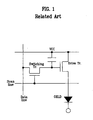
- FIG. 1 is a diagram of circuit for an organic EL display according to a related art
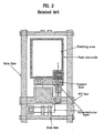
- FIG. 2 is a layout of an organic EL display according to a related art
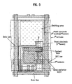
- FIG. 3 is a cross-sectional diagram taken along a cutting line I-I in FIG. 2 .
- a semiconductor layer 2 is formed on a glass substrate 1 with polysilicon and the like.
- the semiconductor layer 2 is then patterned to leave an area for forming a thin film transistor therein.
- a gate insulating layer 3 and a gate electrode conductive layer are sequentially formed over the substrate 1.
- the gate electrode conductive layer is then patterned to form a gate electrode 4.
- Source and drain regions 2a and 2c of a thin film transistor are formed by implanting dopants in the semiconductor layer 2 with B, P or the like using the gate electrode 4 as an implantation mask and performing thermal treatment on the dopant-implanted semiconductor layer 2.
- an undoped portion of the semiconductor layer 2 becomes a channel region 2b.
- an insulating interlayer 5 is formed over the substrate 1.
- the insulating interlayer 5 and the gate insulating layer 3 are then selectively removed to expose the source and drain regions 2a and 2c of the thin film transistor.
- An electrode line 6 is formed to be electrically connected to each of the exposed source and drain regions 2a and 2b.
- a planarizing insulating layer 7 is formed over the substrate.
- the planarizing insulating layer 7 is then selectively removed to expose the electrode line 6 connected to the drain region 2c.
- An anode (pixel electrode) 8 is formed to be electrically connected to the exposed electrode line 6.
- an insulating layer 9 is formed between neighboring anodes 8.
- a hole injection layer 10 a hole transport layer 11, an organic emitting layer, an electron transport layer 13 and an electron injection layer 14 are sequentially formed over the substrate.
- a passivation layer 16 is formed on the cathode 15 to cut off oxygen or moisture.
- the drive circuit occupies most parts of the pixel area to reduce a portion, through which the light can pass, i.e., to lower an aperture ratio.
- the area occupied by the drive circuit in each pixel area is increased more to lower the aperture ratio considerably.
- the present invention is directed to an organic EL display and fabricating method thereof that substantially obviate one or more problems due to limitations and disadvantages of the related art.
- An object of the present invention is to provide an organic EL display and fabricating method thereof, in which light is emitted from a pixel area having a drive circuit formed thereon and by which a aperture ratio can be raised.
- Another object of the present invention is to provide an organic EL display and fabricating method thereof, in which light can be emitted from front and rear sides of one substrate to enable two-way viewings.
- Another object of the present invention is to provide an organic EL display and fabricating method thereof, in which a pair of organic EL displays are simultaneously fabricated on one substrate, by which a corresponding process is simplified, and by which a processing cost is lowered.
- an organic EL display includes a transparent substrate having a plurality of pixel areas wherein each of a plurality of the pixel areas is divided into a first area and a second area, a first organic EL device on the first area of the transparent substrate to emit light to a bottom of the transparent substrate, and a second organic EL device on the second area of the transparent substrate to emit light to a top of the transparent substrate.
- a transistor for driving the first and second organic EL devices is formed in the second area.
- the first and second organic EL devices are electrically connected to a same transistor to be driven.
- the first organic EL device includes a transistor formed in the second area of the transparent substrate, a first anode formed in the first and second areas of the transparent substrate to be electrically connected to the transistor, an organic EL layer formed on the first anode, and a first cathode formed on the organic EL layer in the first area of the transparent substrate.
- the first anode is a transparent electrode having a high work function and the first cathode is a metal electrode having high reflectivity.
- the second organic EL device includes a transistor formed in the second area of the transparent substrate, a second anode formed in the second area of the transparent substrate to be electrically connected to the transistor, an organic EL layer formed on the second anode, and a second cathode formed on the organic EL layer in the second area of the transparent substrate.
- the second anode is a metal electrode having high reflectivity and low work function and the second cathode is a thin metal electrode having transmittance.
- an organic EL display includes a transparent substrate having a plurality of pixel areas wherein each of a plurality of the pixel areas is divided into a first area and a second area, a transistor formed in the second area of the transparent substrate, a first anode formed in the first and second areas of the transparent substrate including the second anode, an organic EL layer formed on the first anode, a first cathode formed on the organic EL layer in the first area of the transparent substrate, and a second anode formed on the organic EL layer in the second area of the transparent substrate.
- a method of fabricating an organic EL display includes the steps of preparing a transparent substrate having a plurality of pixel areas wherein each of a plurality of the pixel areas is divided into a first area and a second area, forming a transistor on the second area of the pixel area of the transparent substrate, forming a first insulating layer on the transparent substrate including the transistor, exposing an electrode of the transistor by removing a predetermined portion of the first insulating layer, forming a second anode on the first insulating layer in the second area of the pixel area to be electrically connected to the exposed electrode of the transistor, forming a first anode on the first insulating layer including the second anode in the first and second areas of the pixel area, forming an organic EL layer over the substrate including the first anode, forming a first cathode on the organic EL layer in the first area of the pixel area, and forming a second cathode on the organic EL layer in the second area of the pixel
- FIG. 1 is a diagram of circuit for an organic EL display according to a related art
- FIG. 2 is a layout of an organic EL display according to a related art
- FIG. 3 is a cross-sectional diagram taken along a cutting line I-I in FIG. 2 ;
- FIG. 4 is a diagram of circuit for an organic EL display according to the present invention.
- FIG. 5 is a layout of an organic EL display according to the present invention.
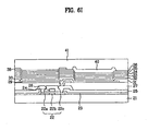
- FIGs. 6A to 6I are cross-sectional diagrams taken along a cutting line II-II in FIG. 5 .
- the concept of the present invention lies in that a top emission type organic EL device is implemented one more using an area occupied by a drive circuit in a pixel area.
- a bottom emission type organic EL device is implemented in an emitting area of a pixel area and a top emission type organic EL device is implemented in a drive circuit area of the pixel area, simultaneously.
- the present invention enables the devices to be independently driven.
- FIG. 4 is a diagram of circuit for an organic EL display according to the present invention
- FIG. 5 is a layout of an organic EL display according to the present invention
- FIGs. 6A to 6I are cross-sectional diagrams taken along a cutting line II-II in FIG. 5 .
- a pixel area of the present invention includes a switching thin film transistor for switching a pixel, a driving thin film transistor for driving the pixel, a storage capacitor, a first anode (pixel electrode), a second anode (pixel electrode), an organic emitting layer, a first cathode (common electrode) and a second cathode (common electrode).
- a transparent substrate of the present invention includes a plurality of pixel areas. Each of a plurality of the pixel areas is divided into a first area and a second area.
- the first area is an emitting area and the second area is a drive circuit area.
- the present invention intends to fabricate the second area, i.e., the drive circuit area into another emitting area.
- a first organic EL device is formed in the first area of the pixel area to emit light to a bottom of the transparent substrate and a second organic EL device is formed in the second area of the pixel area to emit light to a top of the transparent substrate.
- a transistor for driving the first and second organic EL devices is formed in the second area.
- first organic EL device and the second organic EL device can be electrically connected to the same transistor to be driven.
- first and second organic EL devices can be electrically connected to different transistors, respectively.
- the first organic EL device includes the first anode (pixel electrode), an organic EL layer and the first cathode.
- the first anode is formed across the first and second areas of the pixel area to be electrically connected to the transistor.
- the organic EL layer is formed on the first anode.
- the first cathode is formed on the organic EL layer to be formed in the first area of the pixel area.
- the first anode is a transparent electrode formed of ITO or the like to have a high work function.
- the first cathode is formed of a conductive metal electrode having high reflectivity and low work function such as an AL electrode and the like.
- the second organic EL device includes the second anode (pixel electrode), an organic EL layer and the second cathode.
- the second anode is in the second area of the pixel area to be electrically connected to the transistor.
- the organic EL layer is formed on the second anode.
- the second cathode is formed on the organic EL layer to be formed in the second area of the pixel area.
- the second anode is a metal electrode having high reflectivity like Al, Cr, Ag and the like.
- the second cathode is formed of a thin metal electrode having transmittance.
- the second cathode 38 can be formed by depositing Al 1 ⁇ 10nm thick and depositing Ag 1 ⁇ 15nm thick on the Al, by depositing alloy of Mg:Ag or the like 1 ⁇ 15nm thick or by using a conductive material having low conductivity.
- FIGs. 6A to 6I are process cross-sectional diagrams taken along a cutting line II-II in FIG. 5 .
- a transparent substrate having a plurality of pixel areas each of which is divided into a first area (emitting area) and a second area (drive circuit area).
- a semiconductor layer 22 is formed on the second area of the transparent substrate 21 using polysilicon and the like to be utilized as an active layer of a thin film transistor.
- a gate electrode 24 is formed on the gate insulating layer 23.
- impurities or dopants are implanted into the semiconductor layer 22 using the gate electrode 24 as an implantation mask and are then annealed to form a source region 22a and a drain region 22c of the thin film transistor.
- An insulating interlayer 25 is formed on an entire surface of the transparent substrate 21 including the gate electrode 24 and is then patterned to expose portions of the source and drain regions 22a and 22c, respectively.
- electrodes are formed to be electrically connected to the source and drain regions 22a and 22c, respectively to complete the thin film transistor.
- a planarizing layer 27 is formed over the substrate to planarize a surface over the substrate using an insulator.
- the planarizing layer 27 is patterned to form a contact hole 28 exposing a portion of the electrode 26 of the drain region 22c.
- a conductive substance having high reflectivity such as Cr, Al, Ag and the like on the planarizing layer 27 in the second area of the pixel area and is then patterned to form a second anode 29 for top emission.
- a transparent conductive substance having a high work function value such as ITO, IZO and the like is formed on the planarizing layer 27 including the second anode 29 and is then patterned to form a first anode 30 for bottom emission.
- the first anode 30 is formed in the first and second areas of the pixel area.
- an insulating layer 31 is formed over the substrate and is then patterned to remain on an electrical connection area between the second anode 29 and the electrode 26 and on edge areas of the first and second anodes 30 and 29 only.
- a hole injection layer 32, a hole transport layer 33, an organic emitting layer 34, an electron transport layer 35 and an electron injection layer 36 are sequentially formed on the first anode 30 to form an organic EL layer.
- a second cathode 38 for top emission is formed on the electron injection layer 36 in the second area of the pixel area using a first shadow mask 37.
- the second cathode 38 is a thin metal electrode and can be formed by depositing Al 1 ⁇ 10nm thick and depositing Ag 1 ⁇ 15nm thick on the Al, by depositing alloy of Mg:Ag or the like 1 ⁇ 15nm thick or by using a conductive material having low conductivity.
- a first cathode 40 for bottom emission is formed on the electron injection layer 36 in the first area of the pixel area using a second shadow mask 37.
- the first cathode 38 is formed of a conductive material having high reflectivity and low work function such as Al.
- a passivation layer 41 is formed over the substrate to cut of penetration of oxygen or moisture into the organic EL layer. And, a protective cap (not shown in the drawing) is put thereon.
- the present invention provides the following advantages or effects.
- the present invention simplifies the corresponding process to enhance mass productivity and device characteristics.
- the independent drives of the first and second organic EL devices are enabled.
- the present invention enables the fabrication of the display of new concept that enables users to view image from both sides and raises the economical value of the device.
- the present invention enables the implementation of an external display and an internal display using one display module to enable the development of a mobile phone or terminal of low price.
- the present invention uses the related art process conditions to simplify the fabricating process, thereby enhancing mass productivity.
- the present invention enables independent drives of the first and second organic EL devices. Therefore, the present invention can drive the bottom emission and the top emission simultaneously or independently.
- the present invention enables the implementations of displays for internal and external windows using one display module only.
Landscapes
- Engineering & Computer Science (AREA)
- Physics & Mathematics (AREA)
- General Physics & Mathematics (AREA)
- Computer Hardware Design (AREA)
- Theoretical Computer Science (AREA)
- Manufacturing & Machinery (AREA)
- Microelectronics & Electronic Packaging (AREA)
- Electroluminescent Light Sources (AREA)
- Devices For Indicating Variable Information By Combining Individual Elements (AREA)
Claims (15)
- Organische EL-Anzeige, unfassend:- ein transparentes Substrat (21) mit mehreren Pixelbereichen, wobei jeder der mehreren Pixelbereiche in einen ersten Bereich und einen zweiten Bereich unterteilt ist;- eine erste organische EL-Vorrichtung mit einer ersten Anode (30), einer organischen EL-Schicht (32-36), und einer ersten Kathode (40), wobei die erste organische EL-Vorrichtung auf dem ersten Bereich des transparenten Substrats (21) ausgebildet ist, um Licht zu einer Unterseite des transparenten Substrats (21) zu emittieren;- eine zweite organische EL-Vorrichtung mit einer zweiten Anode (29), einer organischen EL-Schicht (32-36), und einer zweiten Kathode (38), wobei die zweite organische EL-Vorrichtung auf dem zweiten Bereich des transparenten Substrats (21) ausgebildet ist, um Licht zu einer Oberseite des transparenten Substrats (21) zu emittieren;- einen Transistor mit einer Elektrode (26), der im zweiten Bereich des transparenten Substrats (21) ausgebildet ist,
dadurch gekennzeichnet, dass- die zweite Anode (29) der zweiten organischen EL-Vorrichtung mit der Elektrode (26) des Transistors verbunden ist, und die zweite Anode (29) auf dem zweiten Bereich ausgebildet ist; und- die erste Anode (30) der ersten organischen EL-Vorrichtung mit der zweiten Anode (29) der zweiten organischen EL-Vorrichtung verbunden ist, und die erste Anode (30) den ersten und den zweiten Bereich bedeckt. - Organische EL-Anzeige nach Anspruch 1, wobei ein Transistor zum Ansteuern der ersten und der zweiten organischen EL-Vorrichtung im zweiten Bereich ausgebildet ist.
- Organische EL-Anzeige nach Anspruch 1, wobei die erste und die zweite organische EL-Vorrichtung elektrisch mit demselben Transistor verbunden sind, um angesteuert zu werden.
- Organische EL-Anzeige nach Anspruch 1, wobei die erste organische EL-Vorrichtung umfasst:- einen Transistor, der im zweiten Bereich des transparenten Substrats (21) ausgebildet ist;- eine erste Anode (30), die im ersten und im zweiten Bereich des transparenten Substrats (21) ausgebildet ist, um elektrisch mit dem Transistor verbunden zu sein;- eine organische EL-Schicht, die auf der ersten Anode (30) ausgebildet ist; und- eine erste Kathode (40), die auf der organischen EL-Schicht im ersten Bereich des transparenten Substrats (21) ausgebildet ist.
- Organische EL-Anzeige nach Anspruch 1, wobei die zweite organische EL-Vorrichtung umfasst:- einen Transistor, der im zweiten Bereich des transparenten Substrats (21) ausgebildet ist;- eine zweite Anode (29), die im zweiten Bereich des transparenten Substrats (21) ausgebildet ist, um elektrisch mit dem Transistor verbunden zu sein;- eine organische EL-Schicht, die auf der zweiten Anode (29) ausgebildet ist; und- eine zweite Kathode (38), die auf der organischen EL-Schicht im zweiten Bereich des transparenten Substrats (21) ausgebildet ist.
- Organische EL-Anzeige, umfassend:- ein transparentes Substrat (21) mit mehreren Pixelbereichen, wobei jeder der mehreren Pixelbereiche in einen ersten Bereich und einen zweiten Bereich unterteilt ist;- einen Transistor, der im zweiten Bereich des transparenten Substrats (21) ausgebildet ist;- eine zweite Anode (29), die im zweiten Bereich des transparenten Substrats (21) ausgebildet ist und mit dem Transistor verbunden ist;- eine erste Anode (30), die im ersten und im zweiten Bereich des transparenten Substrats (21) mit der zweiten Anode (29) ausgebildet ist;- eine organische EL-Schicht (32-36), die auf der ersten Anode (30) ausgebildet ist;- eine erste Kathode (40), die auf der organischen EL-Schicht (32-36) im ersten Bereich des transparenten Substrats (21) ausgebildet ist;- eine zweite Kathode (38), die auf der organischen EL-Schicht (32-36) im zweiten Bereich des transparenten Substrats (21) ausgebildet ist,
dadurch gekennzeichnet, dass- die erste und die zweite Anode (29, 30), die organische EL-Schicht (32-36) und die zweite Kathode (38) im zweiten Bereich des transparenten Substrats ausgebildet sind, um Licht zu einer Oberseite des transparenten Substrats (21) zu emittieren; und- die erste Anode (30), die organische EL-Schicht (32-36) und die erste Kathode (40) im ersten Bereich des transparenten Substrats (21) ausgebildet sind, um Licht zu einer Unterseite des transparenten Substrats (21) zu emittieren. - Organische EL-Anzeige nach Anspruch 4 oder 6, wobei die erste Anode (30) eine transparente Elektrode mit einer hohen Austrittsarbeit ist, und wobei die erste Kathode eine Metallelektrode mit einem hohen Reflexionsvermögen ist.
- Organische EL-Anzeige nach Anspruch 5 oder 6, wobei die zweite Anode (29) eine Metallelektrode mit einem hohen Reflexionsvermögen und geringer Austrittsarbeit ist, und wobei die zweite Kathode (38) eine dünne Metallelektrode mit Transmittanz ist.
- Organische EL-Anzeige nach Anspruch 6, wobei eine Isolationsschicht auf einem elektrischen Verbindungsbereich zwischen dem Transistor und jeder der ersten und zweiten Anoden (30, 29) und auf Randbereichen der ersten und zweiten Anoden (29, 30) ausgebildet ist.
- Verfahren zum Herstellen einer organischen EL-Anzeige mit den Schritten:- Vorbereiten eines transparenten Substrats (21) mit mehreren Pixelbereichen, wobei jeder der mehreren Pixelbereiche in einen ersten Bereich und einen zweiten Bereich unterteilt ist;- Ausbilden eines Transistors auf dem zweiten Bereich des Pixelbereichs des transparenten Substrats (21);- Ausbilden einer ersten Isolationsschicht auf dem transparenten Substrat (21) mit dem Transistor;- Freilegen einer Elektrode des Transistors durch Entfernen eines vorbestimmten Bereichs der ersten Isolationsschicht;- Ausbilden einer zweiten Anode (29) auf der ersten Isolationsschicht im zweiten Bereich des Pixelbereichs, zum elektrischen Verbinden mit der freigelegten Elektrode des Transistors;- Ausbilden einer ersten Anode (30) auf der ersten Isolationsschicht mit der zweiten Anode (29) im ersten und zweiten Bereich des Pixelbereichs;- Ausbilden einer organischen EL-Schicht über dem Substrat mit der ersten Anode (30);- Ausbilden einer ersten Kathode (40) auf der organischen EL-Schicht im ersten Bereich des Pixelbereichs; und- Ausbilden einer zweiten Kathode (39) auf der organischen EL-Schicht im zweiten Bereich des Pixelbereichs.
- Verfahren nach Anspruch 10, wobei im Schritt zum Ausbilden der ersten Anode (30) die erste Anode (30) aus einer transparenten Elektrode mit einer hohen Austrittsarbeit ausgebildet wird, und wobei im Schritt zum Ausbilden der zweiten Anode (29) die zweite Anode (29) aus einer Metallelektrode mit einem hohen Reflexionsvermögen ausgebildet wird.
- Verfahren nach Anspruch 10, wobei im Schritt zum Ausbilden der ersten Kathode (40) die erste Kathode (40) aus einer Metallelektrode mit einem hohen Reflexionsvermögen und geringer Austrittsarbeit ausgebildet wird, und wobei im Schritt zum Ausbilden der zweiten Kathode (38) die zweite Kathode (38) aus einer dünnen Metallelektrode mit Transmittanz ausgebildet wird.
- Verfahren nach Anspruch 12, wobei die zweite Kathode (38) ausgebildet wird, indem Aluminium mit einer Dicke von 1 bis 10 nm und darauf Silber mit einer Dicke von 1 bis 15 nm abgeschieden wird, oder indem eine Verbindung aus Mg:Ag oder Ähnlichem mit einer Dicke von 1 bis 15 nm abgeschieden wird, oder indem eine leitendes Material mit geringer Leitfähigkeit verwendet wird.
- Verfahren nach Anspruch 10, weiter mit einem Schritt zum Ausbilden einer zweiten Isolationsschicht auf einem Bereich, der die zweite Anode (29) mit dem Transistor elektrisch verbindet, und auf Randbereichen der ersten und der zweiten Anode (29, 30).
- Verfahren nach Anspruch 10, wobei der Schritt zum Ausbilden der organischen EL-Schicht die Schritte umfasst:- Ausbilden einer Lochinjektionsschicht über dem Substrat (21) mit der ersten Anode (30);- Ausbilden einer Lochtransportschicht (33) auf der Lochinjektionsschicht (32);- Ausbilden einer Emissionsschicht (34) auf der Lochtransportschicht (33);- Ausbilden einer Elektronentransportschicht (35) auf der Emissionsschicht (34); und- Ausbilden einer Elektroneninjektionsschicht (36) auf der Elektronentransportschicht (35).
Applications Claiming Priority (2)
| Application Number | Priority Date | Filing Date | Title |
|---|---|---|---|
| KR1020040036349A KR100565674B1 (ko) | 2004-05-21 | 2004-05-21 | 양방향 유기 el 디스플레이 패널 및 그 제조 방법 |
| KR2004036349 | 2004-05-21 |
Publications (2)
| Publication Number | Publication Date |
|---|---|
| EP1599073A1 EP1599073A1 (de) | 2005-11-23 |
| EP1599073B1 true EP1599073B1 (de) | 2012-09-26 |
Family
ID=34936752
Family Applications (1)
| Application Number | Title | Priority Date | Filing Date |
|---|---|---|---|
| EP05010964A Expired - Lifetime EP1599073B1 (de) | 2004-05-21 | 2005-05-20 | Organische EL Anzeigevorrichtung und ihr Herstellungsverfahren |
Country Status (5)
| Country | Link |
|---|---|
| US (1) | US7474047B2 (de) |
| EP (1) | EP1599073B1 (de) |
| JP (1) | JP4825451B2 (de) |
| KR (1) | KR100565674B1 (de) |
| CN (1) | CN1700828B (de) |
Families Citing this family (17)
| Publication number | Priority date | Publication date | Assignee | Title |
|---|---|---|---|---|
| EP1505666B1 (de) * | 2003-08-05 | 2018-04-04 | LG Display Co., Ltd. | Nach oben abstrahlende organische elektrolumineszente anzeigevorrichtung mit aktiver matrix und verfahren zu deren herstellung |
| US7420324B2 (en) * | 2004-06-03 | 2008-09-02 | Lg Display Co., Ltd. | Organic EL display and fabricating method thereof |
| JP5066327B2 (ja) * | 2005-06-28 | 2012-11-07 | 株式会社ジャパンディスプレイイースト | 液晶表示装置 |
| US7906765B2 (en) * | 2005-10-06 | 2011-03-15 | Invention Science Fund I | Mote signal energy aspects |
| KR100774949B1 (ko) * | 2005-12-26 | 2007-11-09 | 엘지전자 주식회사 | 전계발광소자와 그 제조방법 |
| KR100864882B1 (ko) | 2006-12-28 | 2008-10-22 | 삼성에스디아이 주식회사 | 유기전계발광표시장치 및 그 제조방법 |
| JP5246071B2 (ja) * | 2009-07-06 | 2013-07-24 | セイコーエプソン株式会社 | 有機el装置、電子機器 |
| KR101084198B1 (ko) * | 2010-02-24 | 2011-11-17 | 삼성모바일디스플레이주식회사 | 유기 발광 표시 장치 |
| WO2012108142A1 (ja) | 2011-02-07 | 2012-08-16 | シャープ株式会社 | 有機el表示装置及びその製造方法 |
| CN103165826B (zh) | 2011-12-19 | 2016-12-28 | 联想(北京)有限公司 | 双面有机发光二极管及其制造方法、显示装置 |
| WO2014071622A1 (zh) | 2012-11-09 | 2014-05-15 | 深圳市柔宇科技有限公司 | 一种双面显示装置及其控制方法 |
| JP6466597B2 (ja) | 2015-04-29 | 2019-02-06 | エーエスエムエル ネザーランズ ビー.ブイ. | サポート装置、リソグラフィ装置およびデバイス製造方法 |
| CN107507573B (zh) * | 2017-10-09 | 2023-07-04 | 深圳市华星光电半导体显示技术有限公司 | Amoled显示装置及其驱动方法 |
| CN111490066B (zh) * | 2019-01-28 | 2022-06-07 | 武汉华星光电半导体显示技术有限公司 | 一种显示面板以及电子装置 |
| CN110047879B (zh) * | 2019-03-28 | 2021-03-16 | 武汉华星光电半导体显示技术有限公司 | 一种显示面板以及电子装置 |
| CN110993658A (zh) * | 2019-11-28 | 2020-04-10 | 深圳市华星光电半导体显示技术有限公司 | 双面oled显示面板及制备方法 |
| WO2023050052A1 (zh) | 2021-09-28 | 2023-04-06 | 京东方科技集团股份有限公司 | 显示基板和显示装置 |
Family Cites Families (11)
| Publication number | Priority date | Publication date | Assignee | Title |
|---|---|---|---|---|
| JP3951968B2 (ja) * | 1997-02-17 | 2007-08-01 | セイコーエプソン株式会社 | 発光装置及びその製造方法 |
| US6462722B1 (en) * | 1997-02-17 | 2002-10-08 | Seiko Epson Corporation | Current-driven light-emitting display apparatus and method of producing the same |
| KR100806212B1 (ko) * | 2000-02-23 | 2008-02-22 | 코닌클리케 필립스 일렉트로닉스 엔.브이. | 아릴-치환 폴리-р-아릴렌비닐렌 |
| JP2002246185A (ja) | 2001-02-22 | 2002-08-30 | Victor Co Of Japan Ltd | 有機エレクトロルミネセンス素子 |
| KR100834343B1 (ko) * | 2001-12-29 | 2008-06-02 | 엘지디스플레이 주식회사 | 유기전기발광소자 |
| KR100845557B1 (ko) * | 2002-02-20 | 2008-07-10 | 삼성전자주식회사 | 액티브 매트릭스형 유기전계발광 표시장치 및 그 제조방법 |
| JP4234376B2 (ja) * | 2002-08-28 | 2009-03-04 | 東芝松下ディスプレイテクノロジー株式会社 | 表示装置及び電子機器 |
| CN100370492C (zh) * | 2002-11-27 | 2008-02-20 | 株式会社半导体能源研究所 | 显示装置及电子设备 |
| EP1589785B1 (de) | 2003-01-24 | 2014-10-15 | Semiconductor Energy Laboratory Co., Ltd. | Lichtemittierendes bauelement, verfahren zu seiner herstellung und elektrische vorrichtung mit einem solchen lichtemittierenden bauelement |
| JP4131838B2 (ja) * | 2003-05-16 | 2008-08-13 | 株式会社半導体エネルギー研究所 | 表示装置 |
| US7622863B2 (en) * | 2003-06-30 | 2009-11-24 | Semiconductor Energy Laboratory Co., Ltd. | Light-emitting device and electronic device including first and second light emitting elements |
-
2004
- 2004-05-21 KR KR1020040036349A patent/KR100565674B1/ko not_active Expired - Lifetime
-
2005
- 2005-05-20 EP EP05010964A patent/EP1599073B1/de not_active Expired - Lifetime
- 2005-05-20 US US11/133,240 patent/US7474047B2/en active Active
- 2005-05-23 CN CN2005100719237A patent/CN1700828B/zh not_active Expired - Lifetime
- 2005-05-23 JP JP2005149891A patent/JP4825451B2/ja not_active Expired - Lifetime
Also Published As
| Publication number | Publication date |
|---|---|
| KR20050111152A (ko) | 2005-11-24 |
| EP1599073A1 (de) | 2005-11-23 |
| KR100565674B1 (ko) | 2006-03-30 |
| JP4825451B2 (ja) | 2011-11-30 |
| US7474047B2 (en) | 2009-01-06 |
| US20050258740A1 (en) | 2005-11-24 |
| JP2005340202A (ja) | 2005-12-08 |
| CN1700828A (zh) | 2005-11-23 |
| CN1700828B (zh) | 2013-04-03 |
Similar Documents
| Publication | Publication Date | Title |
|---|---|---|
| US11778847B2 (en) | Display panel, method for manufacturing same, and display device | |
| EP1599073B1 (de) | Organische EL Anzeigevorrichtung und ihr Herstellungsverfahren | |
| US6958252B2 (en) | Flat panel display device and method of manufacturing the same | |
| KR100909347B1 (ko) | 발광 장치 | |
| US7619359B2 (en) | Organic electroluminescent display having sealant with grains and method for manufacturing the same | |
| EP1603161B1 (de) | Organische elektrolumineszente Anzeigevorrichtung und Herstellungsverfahren | |
| EP1536473B1 (de) | Organische elektrolumineszente Anzeigevorrichtung und Herstellungsverfahren | |
| US7615922B2 (en) | Electro-luminescent display device and method for fabricating the same | |
| US20020149054A1 (en) | Flat panel display device and method of manufacturing the same | |
| US7612377B2 (en) | Thin film transistor array panel with enhanced storage capacitors | |
| US7129524B2 (en) | Organic electroluminescent device and method for fabricating the same | |
| CN1446029A (zh) | 光发射以及其制造方法 | |
| KR100477104B1 (ko) | 발광효율이 개선된 평판표시장치 및 그의 제조방법 | |
| JP2003280555A (ja) | 表示装置および表示装置の製造方法 | |
| US20220140050A1 (en) | Display substrate, fabricating method thereof and display panel | |
| KR100617114B1 (ko) | 듀얼형 유기 el 디스플레이 패널 및 그 제조 방법 | |
| KR100659060B1 (ko) | 유기전계 발광표시장치의 제조방법 | |
| KR20050077202A (ko) | 유기전계발광 표시장치 및 그의 제조방법 | |
| KR20060055846A (ko) | 평판 표시 장치 및 그 제조방법 |
Legal Events
| Date | Code | Title | Description |
|---|---|---|---|
| PUAI | Public reference made under article 153(3) epc to a published international application that has entered the european phase |
Free format text: ORIGINAL CODE: 0009012 |
|
| 17P | Request for examination filed |
Effective date: 20050520 |
|
| AK | Designated contracting states |
Kind code of ref document: A1 Designated state(s): AT BE BG CH CY CZ DE DK EE ES FI FR GB GR HU IE IS IT LI LT LU MC NL PL PT RO SE SI SK TR |
|
| AX | Request for extension of the european patent |
Extension state: AL BA HR LV MK YU |
|
| AKX | Designation fees paid |
Designated state(s): AT BE BG CH CY CZ DE DK EE ES FI FR GB GR HU IE IS IT LI LT LU MC NL PL PT RO SE SI SK TR |
|
| 17Q | First examination report despatched |
Effective date: 20060828 |
|
| RAP1 | Party data changed (applicant data changed or rights of an application transferred) |
Owner name: LG DISPLAY CO., LTD. |
|
| GRAP | Despatch of communication of intention to grant a patent |
Free format text: ORIGINAL CODE: EPIDOSNIGR1 |
|
| RIN1 | Information on inventor provided before grant (corrected) |
Inventor name: KIM, HONG GYU |
|
| GRAS | Grant fee paid |
Free format text: ORIGINAL CODE: EPIDOSNIGR3 |
|
| GRAA | (expected) grant |
Free format text: ORIGINAL CODE: 0009210 |
|
| AK | Designated contracting states |
Kind code of ref document: B1 Designated state(s): AT BE BG CH CY CZ DE DK EE ES FI FR GB GR HU IE IS IT LI LT LU MC NL PL PT RO SE SI SK TR |
|
| REG | Reference to a national code |
Ref country code: GB Ref legal event code: FG4D |
|
| REG | Reference to a national code |
Ref country code: CH Ref legal event code: EP |
|
| REG | Reference to a national code |
Ref country code: AT Ref legal event code: REF Ref document number: 577521 Country of ref document: AT Kind code of ref document: T Effective date: 20121015 |
|
| REG | Reference to a national code |
Ref country code: IE Ref legal event code: FG4D |
|
| REG | Reference to a national code |
Ref country code: DE Ref legal event code: R096 Ref document number: 602005036246 Country of ref document: DE Effective date: 20121122 |
|
| PG25 | Lapsed in a contracting state [announced via postgrant information from national office to epo] |
Ref country code: FI Free format text: LAPSE BECAUSE OF FAILURE TO SUBMIT A TRANSLATION OF THE DESCRIPTION OR TO PAY THE FEE WITHIN THE PRESCRIBED TIME-LIMIT Effective date: 20120926 Ref country code: LT Free format text: LAPSE BECAUSE OF FAILURE TO SUBMIT A TRANSLATION OF THE DESCRIPTION OR TO PAY THE FEE WITHIN THE PRESCRIBED TIME-LIMIT Effective date: 20120926 |
|
| REG | Reference to a national code |
Ref country code: AT Ref legal event code: MK05 Ref document number: 577521 Country of ref document: AT Kind code of ref document: T Effective date: 20120926 |
|
| REG | Reference to a national code |
Ref country code: LT Ref legal event code: MG4D Effective date: 20120926 |
|
| REG | Reference to a national code |
Ref country code: NL Ref legal event code: VDEP Effective date: 20120926 |
|
| PG25 | Lapsed in a contracting state [announced via postgrant information from national office to epo] |
Ref country code: SE Free format text: LAPSE BECAUSE OF FAILURE TO SUBMIT A TRANSLATION OF THE DESCRIPTION OR TO PAY THE FEE WITHIN THE PRESCRIBED TIME-LIMIT Effective date: 20120926 Ref country code: GR Free format text: LAPSE BECAUSE OF FAILURE TO SUBMIT A TRANSLATION OF THE DESCRIPTION OR TO PAY THE FEE WITHIN THE PRESCRIBED TIME-LIMIT Effective date: 20121227 Ref country code: SI Free format text: LAPSE BECAUSE OF FAILURE TO SUBMIT A TRANSLATION OF THE DESCRIPTION OR TO PAY THE FEE WITHIN THE PRESCRIBED TIME-LIMIT Effective date: 20120926 |
|
| PG25 | Lapsed in a contracting state [announced via postgrant information from national office to epo] |
Ref country code: ES Free format text: LAPSE BECAUSE OF FAILURE TO SUBMIT A TRANSLATION OF THE DESCRIPTION OR TO PAY THE FEE WITHIN THE PRESCRIBED TIME-LIMIT Effective date: 20130106 Ref country code: NL Free format text: LAPSE BECAUSE OF FAILURE TO SUBMIT A TRANSLATION OF THE DESCRIPTION OR TO PAY THE FEE WITHIN THE PRESCRIBED TIME-LIMIT Effective date: 20120926 Ref country code: CZ Free format text: LAPSE BECAUSE OF FAILURE TO SUBMIT A TRANSLATION OF THE DESCRIPTION OR TO PAY THE FEE WITHIN THE PRESCRIBED TIME-LIMIT Effective date: 20120926 Ref country code: RO Free format text: LAPSE BECAUSE OF FAILURE TO SUBMIT A TRANSLATION OF THE DESCRIPTION OR TO PAY THE FEE WITHIN THE PRESCRIBED TIME-LIMIT Effective date: 20120926 Ref country code: EE Free format text: LAPSE BECAUSE OF FAILURE TO SUBMIT A TRANSLATION OF THE DESCRIPTION OR TO PAY THE FEE WITHIN THE PRESCRIBED TIME-LIMIT Effective date: 20120926 Ref country code: BE Free format text: LAPSE BECAUSE OF FAILURE TO SUBMIT A TRANSLATION OF THE DESCRIPTION OR TO PAY THE FEE WITHIN THE PRESCRIBED TIME-LIMIT Effective date: 20120926 Ref country code: IS Free format text: LAPSE BECAUSE OF FAILURE TO SUBMIT A TRANSLATION OF THE DESCRIPTION OR TO PAY THE FEE WITHIN THE PRESCRIBED TIME-LIMIT Effective date: 20130126 |
|
| PG25 | Lapsed in a contracting state [announced via postgrant information from national office to epo] |
Ref country code: CY Free format text: LAPSE BECAUSE OF FAILURE TO SUBMIT A TRANSLATION OF THE DESCRIPTION OR TO PAY THE FEE WITHIN THE PRESCRIBED TIME-LIMIT Effective date: 20120926 Ref country code: PT Free format text: LAPSE BECAUSE OF FAILURE TO SUBMIT A TRANSLATION OF THE DESCRIPTION OR TO PAY THE FEE WITHIN THE PRESCRIBED TIME-LIMIT Effective date: 20130128 Ref country code: PL Free format text: LAPSE BECAUSE OF FAILURE TO SUBMIT A TRANSLATION OF THE DESCRIPTION OR TO PAY THE FEE WITHIN THE PRESCRIBED TIME-LIMIT Effective date: 20120926 Ref country code: SK Free format text: LAPSE BECAUSE OF FAILURE TO SUBMIT A TRANSLATION OF THE DESCRIPTION OR TO PAY THE FEE WITHIN THE PRESCRIBED TIME-LIMIT Effective date: 20120926 |
|
| PG25 | Lapsed in a contracting state [announced via postgrant information from national office to epo] |
Ref country code: AT Free format text: LAPSE BECAUSE OF FAILURE TO SUBMIT A TRANSLATION OF THE DESCRIPTION OR TO PAY THE FEE WITHIN THE PRESCRIBED TIME-LIMIT Effective date: 20120926 |
|
| PG25 | Lapsed in a contracting state [announced via postgrant information from national office to epo] |
Ref country code: BG Free format text: LAPSE BECAUSE OF FAILURE TO SUBMIT A TRANSLATION OF THE DESCRIPTION OR TO PAY THE FEE WITHIN THE PRESCRIBED TIME-LIMIT Effective date: 20121226 Ref country code: DK Free format text: LAPSE BECAUSE OF FAILURE TO SUBMIT A TRANSLATION OF THE DESCRIPTION OR TO PAY THE FEE WITHIN THE PRESCRIBED TIME-LIMIT Effective date: 20120926 |
|
| PLBE | No opposition filed within time limit |
Free format text: ORIGINAL CODE: 0009261 |
|
| STAA | Information on the status of an ep patent application or granted ep patent |
Free format text: STATUS: NO OPPOSITION FILED WITHIN TIME LIMIT |
|
| PG25 | Lapsed in a contracting state [announced via postgrant information from national office to epo] |
Ref country code: IT Free format text: LAPSE BECAUSE OF FAILURE TO SUBMIT A TRANSLATION OF THE DESCRIPTION OR TO PAY THE FEE WITHIN THE PRESCRIBED TIME-LIMIT Effective date: 20120926 |
|
| 26N | No opposition filed |
Effective date: 20130627 |
|
| REG | Reference to a national code |
Ref country code: DE Ref legal event code: R097 Ref document number: 602005036246 Country of ref document: DE Effective date: 20130627 |
|
| PG25 | Lapsed in a contracting state [announced via postgrant information from national office to epo] |
Ref country code: MC Free format text: LAPSE BECAUSE OF FAILURE TO SUBMIT A TRANSLATION OF THE DESCRIPTION OR TO PAY THE FEE WITHIN THE PRESCRIBED TIME-LIMIT Effective date: 20120926 |
|
| REG | Reference to a national code |
Ref country code: CH Ref legal event code: PL |
|
| PG25 | Lapsed in a contracting state [announced via postgrant information from national office to epo] |
Ref country code: CH Free format text: LAPSE BECAUSE OF NON-PAYMENT OF DUE FEES Effective date: 20130531 Ref country code: LI Free format text: LAPSE BECAUSE OF NON-PAYMENT OF DUE FEES Effective date: 20130531 |
|
| REG | Reference to a national code |
Ref country code: IE Ref legal event code: MM4A |
|
| PG25 | Lapsed in a contracting state [announced via postgrant information from national office to epo] |
Ref country code: IE Free format text: LAPSE BECAUSE OF NON-PAYMENT OF DUE FEES Effective date: 20130520 |
|
| PG25 | Lapsed in a contracting state [announced via postgrant information from national office to epo] |
Ref country code: TR Free format text: LAPSE BECAUSE OF FAILURE TO SUBMIT A TRANSLATION OF THE DESCRIPTION OR TO PAY THE FEE WITHIN THE PRESCRIBED TIME-LIMIT Effective date: 20120926 |
|
| PG25 | Lapsed in a contracting state [announced via postgrant information from national office to epo] |
Ref country code: LU Free format text: LAPSE BECAUSE OF NON-PAYMENT OF DUE FEES Effective date: 20130520 Ref country code: HU Free format text: LAPSE BECAUSE OF FAILURE TO SUBMIT A TRANSLATION OF THE DESCRIPTION OR TO PAY THE FEE WITHIN THE PRESCRIBED TIME-LIMIT; INVALID AB INITIO Effective date: 20050520 |
|
| REG | Reference to a national code |
Ref country code: FR Ref legal event code: PLFP Year of fee payment: 12 |
|
| REG | Reference to a national code |
Ref country code: FR Ref legal event code: PLFP Year of fee payment: 13 |
|
| REG | Reference to a national code |
Ref country code: FR Ref legal event code: PLFP Year of fee payment: 14 |
|
| PGFP | Annual fee paid to national office [announced via postgrant information from national office to epo] |
Ref country code: GB Payment date: 20240320 Year of fee payment: 20 |
|
| PGFP | Annual fee paid to national office [announced via postgrant information from national office to epo] |
Ref country code: FR Payment date: 20240322 Year of fee payment: 20 |
|
| PGFP | Annual fee paid to national office [announced via postgrant information from national office to epo] |
Ref country code: DE Payment date: 20240320 Year of fee payment: 20 |
|
| REG | Reference to a national code |
Ref country code: DE Ref legal event code: R071 Ref document number: 602005036246 Country of ref document: DE |
|
| REG | Reference to a national code |
Ref country code: GB Ref legal event code: PE20 Expiry date: 20250519 |
|
| PG25 | Lapsed in a contracting state [announced via postgrant information from national office to epo] |
Ref country code: GB Free format text: LAPSE BECAUSE OF EXPIRATION OF PROTECTION Effective date: 20250519 |