EP1600927B1 - Flüssigkristallanzeigevorrichtung und Verfahren zur Steuerung einer solchen Anzeigevorrichtung - Google Patents
Flüssigkristallanzeigevorrichtung und Verfahren zur Steuerung einer solchen Anzeigevorrichtung Download PDFInfo
- Publication number
- EP1600927B1 EP1600927B1 EP04090445A EP04090445A EP1600927B1 EP 1600927 B1 EP1600927 B1 EP 1600927B1 EP 04090445 A EP04090445 A EP 04090445A EP 04090445 A EP04090445 A EP 04090445A EP 1600927 B1 EP1600927 B1 EP 1600927B1
- Authority
- EP
- European Patent Office
- Prior art keywords
- voltage
- gray
- reset
- liquid crystal
- pixel
- Prior art date
- Legal status (The legal status is an assumption and is not a legal conclusion. Google has not performed a legal analysis and makes no representation as to the accuracy of the status listed.)
- Expired - Fee Related
Links
- 239000004973 liquid crystal related substance Substances 0.000 title claims description 100
- 238000000034 method Methods 0.000 title claims description 68
- 239000000758 substrate Substances 0.000 claims description 15
- 230000003287 optical effect Effects 0.000 claims description 10
- 239000011159 matrix material Substances 0.000 claims description 5
- 230000004044 response Effects 0.000 claims description 3
- 230000006870 function Effects 0.000 claims 4
- 239000003990 capacitor Substances 0.000 description 9
- 230000005540 biological transmission Effects 0.000 description 5
- 239000003086 colorant Substances 0.000 description 5
- 238000010586 diagram Methods 0.000 description 4
- 230000005684 electric field Effects 0.000 description 4
- 239000010409 thin film Substances 0.000 description 3
- 230000000694 effects Effects 0.000 description 2
- 238000004519 manufacturing process Methods 0.000 description 2
- 239000000463 material Substances 0.000 description 2
- 230000001360 synchronised effect Effects 0.000 description 2
- 239000000284 extract Substances 0.000 description 1
- 238000012986 modification Methods 0.000 description 1
- 230000004048 modification Effects 0.000 description 1
- 230000000737 periodic effect Effects 0.000 description 1
- 239000000126 substance Substances 0.000 description 1
Images




Classifications
-
- A—HUMAN NECESSITIES
- A47—FURNITURE; DOMESTIC ARTICLES OR APPLIANCES; COFFEE MILLS; SPICE MILLS; SUCTION CLEANERS IN GENERAL
- A47G—HOUSEHOLD OR TABLE EQUIPMENT
- A47G9/00—Bed-covers; Counterpanes; Travelling rugs; Sleeping rugs; Sleeping bags; Pillows
- A47G9/02—Bed linen; Blankets; Counterpanes
- A47G9/0207—Blankets; Duvets
-
- G—PHYSICS
- G09—EDUCATION; CRYPTOGRAPHY; DISPLAY; ADVERTISING; SEALS
- G09G—ARRANGEMENTS OR CIRCUITS FOR CONTROL OF INDICATING DEVICES USING STATIC MEANS TO PRESENT VARIABLE INFORMATION
- G09G3/00—Control arrangements or circuits, of interest only in connection with visual indicators other than cathode-ray tubes
- G09G3/20—Control arrangements or circuits, of interest only in connection with visual indicators other than cathode-ray tubes for presentation of an assembly of a number of characters, e.g. a page, by composing the assembly by combination of individual elements arranged in a matrix no fixed position being assigned to or needed to be assigned to the individual characters or partial characters
- G09G3/34—Control arrangements or circuits, of interest only in connection with visual indicators other than cathode-ray tubes for presentation of an assembly of a number of characters, e.g. a page, by composing the assembly by combination of individual elements arranged in a matrix no fixed position being assigned to or needed to be assigned to the individual characters or partial characters by control of light from an independent source
- G09G3/36—Control arrangements or circuits, of interest only in connection with visual indicators other than cathode-ray tubes for presentation of an assembly of a number of characters, e.g. a page, by composing the assembly by combination of individual elements arranged in a matrix no fixed position being assigned to or needed to be assigned to the individual characters or partial characters by control of light from an independent source using liquid crystals
- G09G3/3611—Control of matrices with row and column drivers
- G09G3/3648—Control of matrices with row and column drivers using an active matrix
-
- G—PHYSICS
- G09—EDUCATION; CRYPTOGRAPHY; DISPLAY; ADVERTISING; SEALS
- G09G—ARRANGEMENTS OR CIRCUITS FOR CONTROL OF INDICATING DEVICES USING STATIC MEANS TO PRESENT VARIABLE INFORMATION
- G09G2310/00—Command of the display device
- G09G2310/02—Addressing, scanning or driving the display screen or processing steps related thereto
- G09G2310/0235—Field-sequential colour display
-
- G—PHYSICS
- G09—EDUCATION; CRYPTOGRAPHY; DISPLAY; ADVERTISING; SEALS
- G09G—ARRANGEMENTS OR CIRCUITS FOR CONTROL OF INDICATING DEVICES USING STATIC MEANS TO PRESENT VARIABLE INFORMATION
- G09G2310/00—Command of the display device
- G09G2310/02—Addressing, scanning or driving the display screen or processing steps related thereto
- G09G2310/0243—Details of the generation of driving signals
- G09G2310/0251—Precharge or discharge of pixel before applying new pixel voltage
-
- G—PHYSICS
- G09—EDUCATION; CRYPTOGRAPHY; DISPLAY; ADVERTISING; SEALS
- G09G—ARRANGEMENTS OR CIRCUITS FOR CONTROL OF INDICATING DEVICES USING STATIC MEANS TO PRESENT VARIABLE INFORMATION
- G09G2310/00—Command of the display device
- G09G2310/06—Details of flat display driving waveforms
- G09G2310/061—Details of flat display driving waveforms for resetting or blanking
-
- G—PHYSICS
- G09—EDUCATION; CRYPTOGRAPHY; DISPLAY; ADVERTISING; SEALS
- G09G—ARRANGEMENTS OR CIRCUITS FOR CONTROL OF INDICATING DEVICES USING STATIC MEANS TO PRESENT VARIABLE INFORMATION
- G09G2330/00—Aspects of power supply; Aspects of display protection and defect management
- G09G2330/02—Details of power systems and of start or stop of display operation
- G09G2330/021—Power management, e.g. power saving
-
- G—PHYSICS
- G09—EDUCATION; CRYPTOGRAPHY; DISPLAY; ADVERTISING; SEALS
- G09G—ARRANGEMENTS OR CIRCUITS FOR CONTROL OF INDICATING DEVICES USING STATIC MEANS TO PRESENT VARIABLE INFORMATION
- G09G2340/00—Aspects of display data processing
- G09G2340/16—Determination of a pixel data signal depending on the signal applied in the previous frame
-
- G—PHYSICS
- G09—EDUCATION; CRYPTOGRAPHY; DISPLAY; ADVERTISING; SEALS
- G09G—ARRANGEMENTS OR CIRCUITS FOR CONTROL OF INDICATING DEVICES USING STATIC MEANS TO PRESENT VARIABLE INFORMATION
- G09G3/00—Control arrangements or circuits, of interest only in connection with visual indicators other than cathode-ray tubes
- G09G3/20—Control arrangements or circuits, of interest only in connection with visual indicators other than cathode-ray tubes for presentation of an assembly of a number of characters, e.g. a page, by composing the assembly by combination of individual elements arranged in a matrix no fixed position being assigned to or needed to be assigned to the individual characters or partial characters
- G09G3/2007—Display of intermediate tones
- G09G3/2011—Display of intermediate tones by amplitude modulation
-
- G—PHYSICS
- G09—EDUCATION; CRYPTOGRAPHY; DISPLAY; ADVERTISING; SEALS
- G09G—ARRANGEMENTS OR CIRCUITS FOR CONTROL OF INDICATING DEVICES USING STATIC MEANS TO PRESENT VARIABLE INFORMATION
- G09G3/00—Control arrangements or circuits, of interest only in connection with visual indicators other than cathode-ray tubes
- G09G3/20—Control arrangements or circuits, of interest only in connection with visual indicators other than cathode-ray tubes for presentation of an assembly of a number of characters, e.g. a page, by composing the assembly by combination of individual elements arranged in a matrix no fixed position being assigned to or needed to be assigned to the individual characters or partial characters
- G09G3/2007—Display of intermediate tones
- G09G3/2014—Display of intermediate tones by modulation of the duration of a single pulse during which the logic level remains constant
-
- G—PHYSICS
- G09—EDUCATION; CRYPTOGRAPHY; DISPLAY; ADVERTISING; SEALS
- G09G—ARRANGEMENTS OR CIRCUITS FOR CONTROL OF INDICATING DEVICES USING STATIC MEANS TO PRESENT VARIABLE INFORMATION
- G09G3/00—Control arrangements or circuits, of interest only in connection with visual indicators other than cathode-ray tubes
- G09G3/20—Control arrangements or circuits, of interest only in connection with visual indicators other than cathode-ray tubes for presentation of an assembly of a number of characters, e.g. a page, by composing the assembly by combination of individual elements arranged in a matrix no fixed position being assigned to or needed to be assigned to the individual characters or partial characters
- G09G3/34—Control arrangements or circuits, of interest only in connection with visual indicators other than cathode-ray tubes for presentation of an assembly of a number of characters, e.g. a page, by composing the assembly by combination of individual elements arranged in a matrix no fixed position being assigned to or needed to be assigned to the individual characters or partial characters by control of light from an independent source
- G09G3/36—Control arrangements or circuits, of interest only in connection with visual indicators other than cathode-ray tubes for presentation of an assembly of a number of characters, e.g. a page, by composing the assembly by combination of individual elements arranged in a matrix no fixed position being assigned to or needed to be assigned to the individual characters or partial characters by control of light from an independent source using liquid crystals
- G09G3/3611—Control of matrices with row and column drivers
- G09G3/3685—Details of drivers for data electrodes
- G09G3/3688—Details of drivers for data electrodes suitable for active matrices only
Definitions
- the present invention relates to a liquid crystal display and a driving method thereof. More particularly, the present invention relates to a field sequential driving type liquid crystal display (FS-LCD) and a driving method thereof.
- FS-LCD field sequential driving type liquid crystal display
- LCD liquid crystal displays
- CRT cathode ray tubes
- An LCD is a display device used to display a desired video signal by applying electric fields to liquid crystal materials having an anisotropic dielectric constant and injected between two substrates, and controlling the strength of electric fields so as to control an amount of light from an external light source (i.e., backlight) transmitted through a substrate.
- an external light source i.e., backlight
- the LCD is representative of portable flat panel displays, and TFT-LCDs using a thin film transistor (TFT) as a switching element are mainly used.
- TFT thin film transistor
- Each pixel in the TFT-LCD can be modeled with capacitors having liquid crystal as a dielectric substance, such as a liquid crystal capacitor.
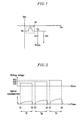
- An equivalent circuit of each pixel in such an LCD is as shown in Fig. 1 .
- each pixel of a liquid crystal display includes a TFT 10, of which a source electrode and a gate electrode are respectively connected to a data line (Dm) and a scanning line (Sn); a liquid crystal capacitor Cl connected between a drain electrode of the TFT and common voltage Vcom; and a storage capacitor Cst connected to the drain electrode of the TFT.
- a scanning signal is applied to a scanning line (Sn) and the TFT 10 is turned on
- data voltages (Vd) supplied to the data line are applied to each pixel electrode (not shown) though the TFT.
- an electric field corresponding to a difference between pixel voltages Vp applied to pixel electrodes and the common voltage Vcom is applied to liquid crystal (which is equivalently shown as the liquid crystal capacitor Cl in Fig. 1 ).
- a pixel voltage Vp needs to be maintained during one frame or one field, so the storage capacitor Cst in Fig. 1 is used to maintain a pixel voltage Vp applied to a pixel electrode.
- liquid crystal display can be classified into two methods, a color filter method and a field sequential driving method, based on methods of displaying color images.
- a liquid crystal display of a color filter method has color filter layers composed of three primary colors such as red R, green G, and blue B in one of two substrates, and displays a desired color by controlling an amount of light transmitted through the color filter layer.
- a liquid crystal display of a color filter method controls an amount of light transmitted through the R, G, and B color filter layers when light from a single light source transmits through the R, G, and B color filter layers, and composes R, G, and B colors to display a desired color.
- a liquid crystal display device displaying color using a single light source and 3 color filter layers needs unit pixels respectively corresponding to each R, G, and B subpixel, thus at least 3 times the number of pixels are needed compared with displaying black and white. Therefore, fine manufacturing techniques are required to produce video images of high definition.
- a field sequential driving type of liquid crystal display sequentially and periodically turns on each independent light source of R, G, and B colors, and adds synchronized color signals corresponding to each pixel based on the lighting periodic time to obtain full colors. That is, according to a field sequential driving type of liquid crystal display, one pixel is not divided into R, G, and B subpixels, and light of 3 primary colors outputted from R, G, and B back lights is sequentially displayed in a time-divisional manner so that the color images are displayed using an after image effect of the eye.
- the field sequential driving method can be classified as an analog driving method and a digital driving method.
- the analog driving method establishes a plurality of gray voltages, selects one gray voltage corresponding to gray data from among the gray voltages, and drives a liquid crystal panel with the selected gray voltage to perform gray display with an amount of transmission corresponding to the gray voltage applied.
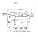
- Fig. 2 shows a driving voltage and amount of light transmission of a conventional liquid crystal display of the analog driving method.
- the driving voltage is a voltage applied to liquid crystal
- optical transmittivity is transmittivity through the liquid crystal. That is, optical transmittivity refers to a torsion degree of the liquid crystal that allows light to transmit.
- a driving voltage having a V11 level is applied to the liquid crystal, and light corresponding to the driving voltage having the V11 level transmits through the liquid crystal in the R field period Tr for displaying an R color.
- a driving voltage having a V12 level is applied to the liquid crystal, and light corresponding to the driving voltage having the V12 level transmits through the liquid crystal in the G field period Tg for displaying a G color.
- a V13 level driving voltage is applied to the liquid crystal, and an amount of light transmission corresponding to the V13 level is obtained.
- a desired color image is displayed by combination of R, G, and B lights transmitted respectively during Tr, Tg, and Tb periods.
- a digital driving method applies a constant driving voltage to the liquid crystal, and controls the voltage applying time to perform a gray display.
- the digital driving method maintains a constant driving voltage, and controls timing of a voltage applying state and a voltage non-applying state, so as to control a total amount of light transmitting through the liquid crystal.
- Fig. 3 shows a waveform which illustrates a driving method of a liquid crystal display of a conventional digital driving method, and shows a waveform of a driving voltage and optical transmittivity of liquid crystal based on driving data of a predetermined bit.
- gray waveform data corresponding to each gray is provided with a digital signal having a predetermined number of bits, for example a 7 bit digital signal, and a gray waveform according to 7 bit data is applied to the liquid crystal.
- Optical transmittivity of the liquid crystal is determined based on the gray waveform applied to perform gray display.
- correct gray is typically not displayed since an effective value response of a desired gray for display (for example, a gray scale of R) is changed by a previous gray display (for example, a gray of G). That is, a pixel voltage Vp actually applied to the liquid crystal is determined by a gray voltage (or a gray waveform) supplied to a present field (for example, an R field) and a gray voltage (or a gray waveform) supplied to the previous field (for example, a B field).
- Fig. 4 shows a field sequential driving method using a reset pulse described in the '063 patent.
- periods (T31 - T36) indicate an R field, a G field, and a B field performing gray display for each of R, G, and B.
- a predetermined voltage (reset voltage) is applied, which is independent of input gray data, and is more than a maximum value of gray data applied during a predetermined time (t31 - t36) at the point where each of the periods (T31 - T36) is ended.
- a state of all the liquid crystals is reset to the same state (for example, a black state in which no light can be transmitted, that is, optical transmittivity is 0) at the point where each of the periods (T31 - T36) is ended.
- a driving method of a liquid crystal display is provided.
- Liquid crystal is disposed between a first substrate and a second substrate, and first, second, and third color lights are sequentially transmitted for each of a plurality of pixels.
- the method includes applying a first voltage corresponding to first gray data to a first said pixel, and applying a second voltage corresponding to second gray data to a second said pixel.
- a first reset voltage corresponding to the first gray data is applied to the first said pixel after applying the first voltage
- a second reset voltage is applied to the second said pixel after applying the second voltage.
- the second reset voltage corresponds to the second gray data and has a voltage level which is different from that of the first reset voltage.
- a driving method of a liquid crystal display is provided.
- Liquid crystal is disposed between a first substrate and a second substrate, and first, second, and third color lights are sequentially transmitted for each of a plurality of pixels.
- the method includes applying a first voltage corresponding to first gray data to a first said pixel, and applying a first reset voltage corresponding to the first gray data to the first said pixel after applying the first voltage, to reset a state of the liquid crystal of the first said pixel to a desired state.
- a driving method of a liquid crystal display includes a plurality of scan lines, and a plurality of data lines insulated and crossing the scan lines.
- a plurality of pixels are formed at areas surrounded by the scan lines and the data lines, and include switches coupled to the scan lines and the data lines, respectively, and are arranged in a matrix format. Red, green, and blue lights are sequentially transmitted for each said pixel.
- the driving method includes transmitting the red, green, and blue lights during a red field, a green field and a blue field, respectively.
- the red field, the green field, and the blue field each includes a reset period for sequentially driving the scan lines, and applying a reset voltage or a reset waveform corresponding to gray data applied during a previous said field; and a data applying period for sequentially driving the scan lines, and applying a gray voltage or a gray waveform corresponding to gray data.
- a liquid crystal display includes a liquid crystal display panel including a plurality of scan lines for transferring scan signals, a plurality of data lines insulated and crossing the scan lines, a plurality of pixels arranged in a matrix format and formed at areas surrounded by the scan lines and the data lines, and including switches coupled to the scan lines and the data lines.
- the liquid crystal display also includes a scan driver for sequentially supplying the scan signals to the scan lines, a gray voltage generator for generating a gray voltage corresponding to gray data, a reset voltage generator for generating a reset voltage corresponding to a gray voltage applied to a previous said pixel, a data driver for supplying the gray voltage and the reset voltage respectively outputted by the gray voltage generator and the reset voltage generator to corresponding said data lines, and a light source for sequentially outputting a first color light, a second color light, and a third color light for each said pixel.
- a scan driver for sequentially supplying the scan signals to the scan lines
- a gray voltage generator for generating a gray voltage corresponding to gray data
- a reset voltage generator for generating a reset voltage corresponding to a gray voltage applied to a previous said pixel
- a data driver for supplying the gray voltage and the reset voltage respectively outputted by the gray voltage generator and the reset voltage generator to corresponding said data lines
- a light source for sequentially outputting a first color light
- Fig. 1 shows a diagram for a pixel of a conventional TFT-LCD.
- Fig. 2 shows a waveform which illustrates a driving method of a liquid crystal display by a conventional analog method.
- Fig. 3 shows a waveform which illustrates a driving method of a liquid crystal display by a conventional digital method.
- Fig. 4 shows a waveform which illustrates a reset driving method of a conventional liquid crystal display device.
- Fig. 5 shows a diagram for a reset driving method according to an exemplary embodiment of the present invention.
- Fig. 6 shows a driving method of a liquid crystal display according to a first exemplary embodiment of the present invention.
- Figs. 7 and 8 show a liquid crystal display according to the first exemplary embodiment.
- Fig. 9 shows a driving method of a liquid crystal display according to a second exemplary embodiment.
- Figs. 10 ⁇ 12 show a liquid crystal display according to the second exemplary embodiment.
- Fig. 13 shows a driving method of a liquid crystal display according to a third exemplary embodiment.
- Fig. 14 illustrates a conceptual diagram of a pixel of a TFT-LCD.
- present pixel refers to a pixel at the present time (t)
- previous pixel or “previous said pixel” refers to a pixel at the previous time (t-1).
- Reset refers to applying a voltage (or waveform) to make liquid crystal materials in an LCD be in a black state such that light transmission is not allowed.
- Gram voltage and reset voltage are voltages having different voltage levels from each other
- gray waveform and “reset waveform” are waveforms having different sizes from each other with respect to on-voltage width and off-voltage width.
- Optical transmittivity refers to a ratio of the transmitted light to the applied light, when a constant light is applied to liquid crystal
- an “amount of light transmitted” refers to an amount of light transmitted through the liquid crystal when light is applied.
- Fig. 5 shows a reset driving method according to an exemplary embodiment of the present invention.
- the R field, G field, and B field display light corresponding to R, G, and B, respectively.
- the R field, G field, and B field are respectively composed of reset periods Rreset, Greset, and Breset and data periods Rdata, Gdata, and Bdata.
- a reset voltage (or a reset waveform) is applied to return a state of the liquid crystals modified by a previously displayed gray to the same state (black state).
- reset voltages (or reset waveforms) corresponding to previous gray data are sequentially applied to each scan line (S1, S2, ... Sn) to allow liquid crystals to be in the same state regardless of a previous gray.
- gray voltages (or gray waveforms) corresponding to a present gray are applied.
- Backlights are sequentially turned on during the data period to output light corresponding to R, G, and B.
- an emission diode is used to provide backlighting, by way of example.
- the present invention is not limited to using emission diodes. Instead, any suitable light source may be used to provide backlighting.
- the driving method of the first exemplary embodiment relates to a reset driving method applied to a field sequential driving method of an analog method.
- a reset voltage (Vr2) applied to an (m,j) pixel that is, a pixel corresponding to the Dm data line and the Sj scan line
- a reset voltage (Vr1) applied to an (m,j+1) pixel that is, a pixel corresponding to the Dm data line and the Sj+1 scan line
- Vr2 and Vr1 applied to an (m,j+1) pixel that is, a pixel corresponding to the Dm data line and the Sj+1 scan line
- a relatively low absolute value of voltage for example, 1V
- a state of liquid crystal is turned to a state in which a relatively large amount of light can transmit (that is, optical transmittivity is high) at the end of the period for applying a data voltage. Therefore, a relatively large absolute value of reset voltage should be applied to the present pixel.
- a constant reset voltage is applied regardless of the data voltage applied to the previous pixel, and enough reset voltage to reset all liquid crystals is applied.
- the problem with such a method of applying a constant reset voltage is that consumption of power by the reset voltage is increased.
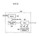
- Figs. 7 and 8 show a liquid crystal display for applying a reset voltage according to the first exemplary embodiment.
- a liquid crystal display includes a liquid crystal display panel 100, a scan driver 200, a data driver 300, a gray voltage generator 400, a timing controller 500, a reset voltage generator 600, emission diodes 700a, 700b, and 700c outputting R, G, and B lights respectively, and a light source controller 800.
- a plurality of scan lines 102 are formed, and data lines 104 that are insulated and crossing the plurality of scan lines for transferring gray data and reset voltages are formed.
- a plurality of pixels 110 arranged in a matrix format are respectively surrounded by scan lines and data lines, each pixel including a thin film transistor (not shown) of which a corresponding scan line and a corresponding data line are respectively connected to a gate electrode and a source electrode, and a pixel capacitor (not shown) and a storage capacitor (not shown) connected to a drain electrode of the thin film transistor.
- the scan driver 200 sequentially applies scan signals to scan lines, allowing the TFTs of which gate electrodes are connected to the scan lines to be turned on. According to the exemplary embodiment, first, the scan driver 200 sequentially applies scan signals for applying a reset voltage to the plurality of scan lines so as to erase an effect of a data voltage applied to a previous pixel, and sequentially applies scan signals for applying data voltages to the plurality of scan lines.
- the timing controller 500 receives gray data signals R, G, and B data, and horizontal synchronizing signals (Hsync) and vertical synchronizing signals (Vsync), and supplies necessary control signals Sg, Sd, and Sb to the scan driver 200, the data driver 300, and the light source controller 800, respectively, and supplies gray data R, G, and B data to the gray voltage generator 400 and the reset voltage generator 600.
- Hsync horizontal synchronizing signals
- Vsync vertical synchronizing signals
- the gray voltage generator 400 generates gray voltages corresponding to gray data which is supplied to the data driver 300.
- the reset voltage generator 600 selects reset voltages corresponding to the gray voltages to be applied to a previous pixel, and supplies the selected voltage to the data driver 300.
- the data driver 300 applies gray voltages outputted from the gray voltage generator 400, or reset voltages outputted from the reset voltage generator 600, to corresponding data lines.
- the emission diodes 700a, 700b, and 700c output light corresponding to each R, G, and B to the LCD panel 100, and the light source controller 800 controls lighting time of the emission diodes 700a, 700b, and 700c.
- points of time for supplying corresponding gray data to the data lines and lighting R, G, and B emission diodes by the light source controller 800 can be synchronized with control signals provided from the timing controller 500.
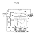
- the reset voltage generator 600 includes a memory 620, a reset voltage selector 640, a switch 660, and a constant voltage generator 680.
- the memory 620 stores gray data corresponding to a previous pixel and reset voltage values corresponding to the previous pixel.
- the reset voltage selector 640 reads reset voltage values corresponding to gray data R, G, and B of the previous pixel stored in the memory 620, and controls operation of the switch 660.
- the constant voltage generator 680 generates reset voltages Vr1, Vr2, and 0V which are supplied to the switch 660.
- the switch 660 selects one reset voltage of a plurality of reset voltages outputted from the constant voltage generator 680 according to control operation of the reset voltage selector 640, which is outputted to the data driver 300.
- the reset voltage generator 600 generates different sizes of reset voltages based on data voltages applied to previous pixels, and the data driver 300 applies reset voltages corresponding to previous gray data outputted from the reset voltage generator 600 to data lines.
- the most suitable voltage for reset can be applied so that power consumption by reset voltages can be reduced.
- a driving method of the second exemplary embodiment relates to a reset driving method applied to a field sequential driving method of a digital method.
- the width of a reset waveform (tr1) applied to an (m,j) pixel that is, a pixel corresponding to the Dm data line and the Sj scan line
- the width of a reset waveform (tr2) applied to an (m,j+1) pixel that is, a pixel corresponding to the Dm data line and the Sj+1 scan line
- a previous pixel for example, a pixel for displaying B light
- the state of the liquid crystal in the normally white mode, in the case a waveform with a large voltage width is applied to a previous pixel, the state of the liquid crystal is turned to a state such that a relatively lesser amount of light can transmit than with a waveform to which a small voltage width is applied, thus a waveform with a small voltage width can be applied.
- different widths of reset waveforms are applied based on a width (or pattern) of a gray waveform applied to a previous pixel, and hence consumption of power by reset waveforms can be reduced or minimized.
- Figs. 10 ⁇ 12 show a liquid crystal display for applying a reset waveform according to the second exemplary embodiment.
- a liquid crystal display according to the second exemplary embodiment shown in Fig. 10 parts that are the same as parts of a liquid crystal display according to the first exemplary embodiment shown in Fig. 7 have the same reference numerals, and redundant explanations are not provided.
- a gray waveform generator 900 generates a gray waveform having a voltage width corresponding to gray data (i.e., R, G, B data), and supplies the gray waveform to the data driver 300.
- the reset waveform generator 1000 generates reset waveforms corresponding to gray waveforms applied to a previous pixel and supplies the generated reset waveforms to the data driver 300.
- the data driver 300 applies a gray waveform outputted by the gray waveform generator 900, or a reset waveform outputted by the reset waveform generator 1000 to corresponding data lines.
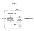
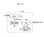
- Figs. 11 and 12 respectively show the gray waveform generator 900 and the reset waveform generator 1000 according to the secondary exemplary embodiment.
- the gray waveform generator 900 includes a voltage applying time controller 920, a pattern table 940, a constant voltage generator 960, and a switch 980.
- the pattern table 940 stores gray waveform patterns (on/off patterns) corresponding to gray data.
- the pattern table stores a 4 bit on/off pattern corresponding to 6 bit gray data.
- the pattern table stores 1011 on/off patterns (here, "1" is on waveform, and "0" is off waveform) corresponding to 6 bit gray data of 101111.
- the voltage applying time controller 920 extracts gray waveform patterns (on/off patterns) corresponding to input gray data R, G, and B from the pattern table, and controls on/off operation and on/off time of the switch 980 based on extracted gray waveform pattern.
- the voltage applying time controller 920 controls the switch 980 to allow the first voltage (Von) to be applied so as to turn on the state of liquid crystal during the predetermined time, when the extracted gray waveform patterns (on/off) pattern value is "1".
- the voltage applying time controller 920 controls the switch 980 to allow the second voltage (0 V) to be applied so as to turn off the state of liquid crystal, when the extracted gray waveform patterns (on/off) pattern value is "0".
- the constant voltage generator 960 generates the first voltage (Von) and the second voltage (0 V) which are supplied to the switch 980.
- the switch 980 selects the first voltage or the second voltage outputted from the constant voltage generator 960 based on a control operation of the voltage applying time controller 920, and outputs a corresponding gray waveform to the data driver 300.
- the reset waveform generator 1000 includes a memory 1040, a voltage applying time controller 1020, a constant voltage generator 1060, and a switch 1080.
- the memory 1040 stores gray data corresponding to a previous pixel, and a reset waveform corresponding to previous gray data.
- the memory 1040 stores a 3 bit reset waveform pattern (on/off pattern) corresponding to 6 bit gray data.
- the memory stores an on/off pattern 100 (here, "1" is on waveform, and "0" is off waveform) corresponding to 6 bit gray data of 101111.
- the voltage application controller 1020 reads reset waveform patterns (on/off pattern) corresponding to gray data R, G, and B of a previous pixel stored in the memory 1040, and controls an on/off operation and an on/off time of the switch 1080 according to the on/off pattern read.
- the switch 1080 and the constant voltage generator 1060 shown in Fig. 12 operate in similar manner as the corresponding elements shown in Fig. 11 . Therefore, redundant explanations are not provided.
- the driving method of the third exemplary embodiment relates to a reset driving method applied to a field sequential driving method of a digital method.
- a voltage (V1) applied to an (m,j) pixel that is, a pixel corresponding to the Dm data line and the Sj scan line
- a reset voltage (V2) applied to an (m,j+1) pixel that is, a pixel corresponding to the Dm data line and the Sj+1 scan line
- V1 and V2 respectively applied to an (m,j+1) pixel for displaying a present R light
- a previous pixel for example, a pixel for displaying B light
- a normally white mode in the case a large voltage width (td1) is applied to a previous pixel, the state of liquid crystal is turned to a state in which relatively lesser light can transmit than with a waveform with a small voltage width (td2) applied, thus a reset waveform with small voltage (V1) can be applied.
- the reset voltage may not need to be applied.
- different sizes of reset voltages are applied based on a width (or pattern) of the gray waveform applied to a previous pixel, and consumption of power by reset voltages can therefore be reduced or minimized.
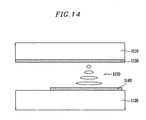
- Fig. 14 illustrates a conceptual diagram of a pixel of a TFT-LCD.
- the pixel includes a liquid crystal 1150 disposed between a first substrate 1110 and a second substrate 1120, a first electrode (common electrode) 1130 arranged at the first substrate 1110, and a second electrode (pixel electrode) 1140 arranged at the second substrate 1120.
- a first electrode common electrode
- a second electrode pixel electrode
- Exemplary embodiments of the present invention can be applied to the pixel of Fig. 14 , as well as other suitable pixels.
- the first and second substrates 1110, 1120 and the liquid crystal 1150 may be equivalently represented, for example, as the liquid crystal capacitor Cl in Fig. 1 .
Landscapes
- Engineering & Computer Science (AREA)
- Chemical & Material Sciences (AREA)
- Crystallography & Structural Chemistry (AREA)
- Physics & Mathematics (AREA)
- Computer Hardware Design (AREA)
- General Physics & Mathematics (AREA)
- Theoretical Computer Science (AREA)
- Control Of Indicators Other Than Cathode Ray Tubes (AREA)
- Liquid Crystal Display Device Control (AREA)
- Liquid Crystal (AREA)
Claims (12)
- Ein Ansteuerverfahren einer Flüssigkristallanzeige, wobei ein Flüssigkristall (1150) zwischen einem ersten Substrat (1110) und einem zweiten Substrat (1120) angeordnet ist, um eine Vielzahl von Pixeln (110) zu definieren, und Licht einer ersten, zweiten und dritten Farbe sequenziell durch die Vielzahl von Pixeln (110) transmittiert wird, umfassend:(a) Anlegen einer ersten Spannung, die ersten Graudaten entspricht, an ein erstes Pixel; und(b) Anlegen einer ersten konstanten Rücksetzspannung, deren Betrag als eine Funktion der ersten Graudaten bestimmt wird, an das erste Pixel nach Schritt (a), um den Zustand des Flüssigkristalls des ersten Pixels in einen gewünschten Zustand zurückzusetzen.
- Das Ansteuerverfahren einer Flüssigkristallanzeige nach Anspruch 1, ferner folgende Schritte umfassend:(c) Anlegen einer zweiten Spannung, die zweiten Graudaten entspricht, an ein zweites Pixel und(d) Anlegen einer zweiten konstanten Rücksetzspannung an das zweite Pixel nach Schritt (c), wobei die zweite Rücksetzspannung als eine Funktion der zweiten Graudaten bestimmt wird und ein Spannungsniveau aufweist, das sich von dem der ersten Rücksetzspannung unterscheidet.
- Das Ansteuerverfahren einer Flüssigkristallanzeige nach Anspruch 2, wobei die erste Rücksetzspannung geringer als die zweite Rücksetzspannung ist, wenn die erste Grauspannung größer als die zweite Grauspannung ist.
- Das Ansteuerverfahren einer Flüssigkristallanzeige nach Anspruch 1, wobei die erste Farbe, zweite Farbe und dritte Farbe rote Farbe, grüne Farbe beziehungsweise blaue Farbe sind.
- Das Ansteuerverfahren einer Flüssigkristallanzeige nach Anspruch 1, wobei der gewünschte Zustand des Flüssigkristalls ein Zustand ist, in dem die optische Durchlässigkeit ungefähr Null ist.
- Das Ansteuerverfahren einer Flüssigkristallanzeige nach Anspruch 1, wobei in Schritt (b) die den ersten Graudaten entsprechende erste Rücksetzspannung angelegt wird, wenn die erste Grauspannung geringer als eine Bezugsspannung ist, und keine Rücksetzspannung angelegt wird, wenn die erste Grauspannung größer als die Bezugsspannung ist.
- Das Ansteuerverfahren einer Flüssigkristallanzeige nach Anspruch 6, wobei die Bezugsspannung eine Spannung ist, die die optische Durchlässigkeit ungefähr Null werden lässt.
- Das Ansteuerverfahren einer Flüssigkristallanzeige nach Anspruch 1, wobei Schritt (b) umfasst:Auswählen der ersten Rücksetzspannung aus mindestens zwei vorbestimmten Rücksetzspannungen als Antwort auf die ersten Graudaten; undBereitstellen der ersten Rücksetzspannung an das erste Pixel.
- Das Ansteuerverfahren einer Flüssigkristallanzeige nach Anspruch 1, wobei die Flüssigkristallanzeige eine Vielzahl von Abtastleitungen (102), eine Vielzahl von Datenleitungen (104), die von den Abtastleitungen isoliert sind und diese kreuzen, beinhaltet, wobei besagte Vielzahl von Pixeln (110) in einem Matrixformat angeordnet sind, wobei jedes Pixel an einem Bereich ausgebildet ist, der von einer der Abtastleitungen und einer besagter Datenleitungen umgeben ist, und einen Schalter, der mit einer Abtastleitung beziehungsweise einer Datenleitung verbunden ist, sowie eine Elektrode des Pixels beinhaltet, wobei das Ansteuerverfahren sequenzielles Transmittieren des roten, grünen und blauen Lichts während eines roten Feldes, eines grünen Feldes beziehungsweise eines blauen Feldes umfasst, wobei das rote Feld, das grüne Feld und das blaue Feld jeweils Folgendes umfassen:einen Rücksetz-Zeitabschnitt zum sequenziellen Ansteuern der Abtastleitungen und Anlegen der ersten Rücksetzspannung an das erste Pixel, das der ersten Spannung, während des direkt vorangehenden Feldes an das besagte erste Pixel angelegt wird, entspricht; undeinen Datenanlege-Zeitabschnitt zum sequenziellen Ansteuern der Abtastleitungen und Anlegen der ersten Spannung an das erste Pixel, die Graudaten des Feldes entspricht.
- Das Ansteuerverfahren einer Flüssigkristallanzeige nach Anspruch 9, wobei das Verfahren umfasst: Auswählen der ersten Rücksetzspannung, die der ersten, während des direkt vorangehenden Feldes an das erste Pixel angelegten Spannung entspricht, aus mindestens zwei vorbestimmten Rücksetzspannungen mit verschiedenen Spannungsniveaus sowie Anlegen der ersten Rücksetzspannung an das erste Pixel während des Rücksetz-Zeitabschnittes.
- Eine Flüssigkristallanzeige, umfassend:eine Flüssigkristallanzeigetafel (100), umfassend eine Vielzahl von Abtastleitungen (102) zum Übertragen von Abtastsignalen, eine Vielzahl von Datenleitungen (104), die von den Abtastleitungen isoliert sind und diese kreuzen, sowie eine Vielzahl von in einem Matrixformat angeordneten Pixeln (110), wobei jedes Pixel an einem Bereich ausgebildet ist, der von einer der Abtastleitungen und einer der Datenleitungen umgeben ist, und einen Schalter beinhaltet, der mit der Abtastleitung, der Datenleitung und einer Elektrode des Pixels verbunden ist;einen Abtasttreiber (200) zum sequenziellen Bereitstellen der Abtastsignale an die Abtastleitungen;einen Grauspannungsgenerator (400) zum Generieren einer Graudaten entsprechenden Grauspannung;einen Rücksetzspannungsgenerator (600) zum Generieren einer Rücksetzspannung als Funktion der vorher an das Pixel angelegten Grauspannung bestimmt ist;einen Datentreiber (300) zum Bereitstellen der Grauspannung und der Rücksetzspannung, die von dem Grauspannungsgenerator (400) beziehungsweise von dem Rücksetzspannungsgenerator (600) an entsprechende Datenleitungen ausgegeben werden, und eine Lichtquelle zum sequenziellen Ausgeben von Licht einer ersten Farbe, einer zweiten Farbe und einer dritten Farbe für jedes Pixel.
- Die Flüssigkristallanzeige nach Anspruch 11, wobei der Rücksetzspannungsgenerator (600) umfasst:einen Speicher (620) zum Speichern der Graudaten, die der vorher an das Pixel angelegten Grauspannung entsprechen, sowie eines als Funktion der Grauspannung bestimmten Rücksetzspannungswertes;einen Konstantspannungsgenerator (680) zum Generieren mindestens zweier vorbestimmter Rücksetzspannungen mit verschiedenen Spannungsniveaus;einen Schalter (660) zum Auswählen der Rücksetzspannung aus den mindestens zwei von dem Konstantspannungsgenerator generierten vorbestimmten Rücksetzspannungen; undeinen Rücksetzspannungswähler (640) zum Lesen des Rücksetzspannungswertes, der der vorher angelegten Grauspannung entspricht, aus dem Speicher und Steuern eines Betriebes des Schalters auf der Grundlage des aus dem Speicher gelesenen Rücksetzspannungswertes.
Priority Applications (1)
| Application Number | Priority Date | Filing Date | Title |
|---|---|---|---|
| EP06126624A EP1772848B1 (de) | 2004-05-17 | 2004-11-17 | Flüssigkristallanzeigevorrichtung und Verfahren zur Steuerung einer solchen Anzeigevorrichtung |
Applications Claiming Priority (2)
| Application Number | Priority Date | Filing Date | Title |
|---|---|---|---|
| KR2004034678 | 2004-05-17 | ||
| KR10-2004-0034678A KR100536222B1 (ko) | 2004-05-17 | 2004-05-17 | 액정 표시 장치 및 이의 구동방법 |
Related Child Applications (2)
| Application Number | Title | Priority Date | Filing Date |
|---|---|---|---|
| EP06126624A Division EP1772848B1 (de) | 2004-05-17 | 2004-11-17 | Flüssigkristallanzeigevorrichtung und Verfahren zur Steuerung einer solchen Anzeigevorrichtung |
| EP06126624.3 Division-Into | 2006-12-20 |
Publications (2)
| Publication Number | Publication Date |
|---|---|
| EP1600927A1 EP1600927A1 (de) | 2005-11-30 |
| EP1600927B1 true EP1600927B1 (de) | 2010-04-28 |
Family
ID=34928845
Family Applications (2)
| Application Number | Title | Priority Date | Filing Date |
|---|---|---|---|
| EP04090445A Expired - Fee Related EP1600927B1 (de) | 2004-05-17 | 2004-11-17 | Flüssigkristallanzeigevorrichtung und Verfahren zur Steuerung einer solchen Anzeigevorrichtung |
| EP06126624A Expired - Fee Related EP1772848B1 (de) | 2004-05-17 | 2004-11-17 | Flüssigkristallanzeigevorrichtung und Verfahren zur Steuerung einer solchen Anzeigevorrichtung |
Family Applications After (1)
| Application Number | Title | Priority Date | Filing Date |
|---|---|---|---|
| EP06126624A Expired - Fee Related EP1772848B1 (de) | 2004-05-17 | 2004-11-17 | Flüssigkristallanzeigevorrichtung und Verfahren zur Steuerung einer solchen Anzeigevorrichtung |
Country Status (6)
| Country | Link |
|---|---|
| US (1) | US7429971B2 (de) |
| EP (2) | EP1600927B1 (de) |
| JP (1) | JP2005331907A (de) |
| KR (1) | KR100536222B1 (de) |
| CN (1) | CN100437233C (de) |
| DE (2) | DE602004026835D1 (de) |
Families Citing this family (20)
| Publication number | Priority date | Publication date | Assignee | Title |
|---|---|---|---|---|
| TWI346927B (en) * | 2006-09-15 | 2011-08-11 | Au Optronics Corp | Driving method of a liquid crystal display |
| CN100465710C (zh) * | 2006-10-10 | 2009-03-04 | 友达光电股份有限公司 | 液晶显示器的驱动方法 |
| TWI349252B (en) * | 2006-11-29 | 2011-09-21 | Novatek Microelectronics Corp | Display devices and driving methods thereof |
| KR101363669B1 (ko) * | 2006-12-26 | 2014-02-14 | 엘지디스플레이 주식회사 | 액정표시장치 및 그의 구동 방법 |
| TW200847092A (en) * | 2007-05-17 | 2008-12-01 | Himax Display Inc | Method for driving liquid crystal display |
| CN101329845B (zh) * | 2007-06-19 | 2011-01-12 | 立景光电股份有限公司 | 液晶显示器及其驱动方法 |
| CN101334968A (zh) * | 2007-06-26 | 2008-12-31 | 立景光电股份有限公司 | 液晶显示器的驱动方法 |
| US20100007591A1 (en) * | 2008-07-10 | 2010-01-14 | Himax Display, Inc. | Pixel unit for a display device and driving method thereof |
| CN102376262B (zh) * | 2010-08-17 | 2015-07-08 | 上海天马微电子有限公司 | 电子墨水显示面板及其驱动方法和驱动装置 |
| KR20120049022A (ko) * | 2010-11-08 | 2012-05-16 | 삼성모바일디스플레이주식회사 | 액정 표시 장치 및 그의 구동 방법 |
| US9196186B2 (en) * | 2011-04-08 | 2015-11-24 | Sharp Kabushiki Kaisha | Display device and method for driving display device |
| KR101941984B1 (ko) * | 2011-09-27 | 2019-04-12 | 삼성디스플레이 주식회사 | 액정표시장치 |
| CN104299575B (zh) * | 2013-12-13 | 2017-01-11 | 天津三星电子有限公司 | 一种时序混色的显示控制方法、装置及显示器 |
| KR102527844B1 (ko) * | 2018-07-16 | 2023-05-03 | 삼성디스플레이 주식회사 | 전원 전압 생성 회로 및 이를 포함하는 표시 장치 |
| CN111613188B (zh) * | 2020-06-28 | 2023-08-25 | 京东方科技集团股份有限公司 | 显示面板的驱动方法、显示面板及显示装置 |
| KR102831247B1 (ko) * | 2020-11-17 | 2025-07-07 | 엘지디스플레이 주식회사 | 표시 장치 |
| CN112700749B (zh) * | 2021-01-04 | 2022-04-26 | 武汉天马微电子有限公司 | 显示面板的驱动方法及其驱动装置、显示装置 |
| CN114187871B (zh) * | 2021-12-10 | 2023-03-21 | 北京欧铼德微电子技术有限公司 | 电压调整方法及装置、电子设备 |
| CN116030750B (zh) * | 2023-01-18 | 2026-08-07 | 合肥维信诺科技有限公司 | 一种显示装置的驱动方法及显示装置 |
| JP2025110530A (ja) * | 2024-01-16 | 2025-07-29 | 株式会社Magnolia White | 表示装置 |
Family Cites Families (8)
| Publication number | Priority date | Publication date | Assignee | Title |
|---|---|---|---|---|
| US6078303A (en) * | 1996-12-19 | 2000-06-20 | Colorado Microdisplay, Inc. | Display system having electrode modulation to alter a state of an electro-optic layer |
| JP3371200B2 (ja) * | 1997-10-14 | 2003-01-27 | 富士通株式会社 | 液晶表示装置の表示制御方法及び液晶表示装置 |
| JPH11296150A (ja) * | 1998-04-10 | 1999-10-29 | Masaya Okita | 液晶の高速駆動方法 |
| JP4806865B2 (ja) * | 2001-07-16 | 2011-11-02 | パナソニック株式会社 | 液晶表示装置 |
| JP3804502B2 (ja) * | 2001-09-27 | 2006-08-02 | カシオ計算機株式会社 | 液晶表示装置の駆動方法 |
| JP3928438B2 (ja) * | 2001-11-30 | 2007-06-13 | コニカミノルタホールディングス株式会社 | 液晶表示素子の駆動方法、駆動装置及び液晶表示装置 |
| JP2003345314A (ja) * | 2002-05-28 | 2003-12-03 | Casio Comput Co Ltd | フィールドシーケンシャル液晶表示装置の駆動方法 |
| TWI256028B (en) * | 2002-10-08 | 2006-06-01 | Rohm Co Ltd | Organic EL element drive circuit and organic EL display device using the same drive circuit |
-
2004
- 2004-05-17 KR KR10-2004-0034678A patent/KR100536222B1/ko not_active Expired - Fee Related
- 2004-10-06 JP JP2004293633A patent/JP2005331907A/ja active Pending
- 2004-11-02 US US10/980,686 patent/US7429971B2/en not_active Expired - Fee Related
- 2004-11-17 DE DE602004026835T patent/DE602004026835D1/de not_active Expired - Lifetime
- 2004-11-17 EP EP04090445A patent/EP1600927B1/de not_active Expired - Fee Related
- 2004-11-17 EP EP06126624A patent/EP1772848B1/de not_active Expired - Fee Related
- 2004-11-17 DE DE602004025153T patent/DE602004025153D1/de not_active Expired - Lifetime
- 2004-11-18 CN CNB2004100947811A patent/CN100437233C/zh not_active Expired - Fee Related
Also Published As
| Publication number | Publication date |
|---|---|
| EP1600927A1 (de) | 2005-11-30 |
| EP1772848A3 (de) | 2007-04-25 |
| US20050253796A1 (en) | 2005-11-17 |
| DE602004026835D1 (de) | 2010-06-10 |
| EP1772848B1 (de) | 2010-01-13 |
| KR20050109698A (ko) | 2005-11-22 |
| CN1700061A (zh) | 2005-11-23 |
| EP1772848A2 (de) | 2007-04-11 |
| US7429971B2 (en) | 2008-09-30 |
| KR100536222B1 (ko) | 2005-12-12 |
| DE602004025153D1 (de) | 2010-03-04 |
| CN100437233C (zh) | 2008-11-26 |
| JP2005331907A (ja) | 2005-12-02 |
Similar Documents
| Publication | Publication Date | Title |
|---|---|---|
| EP1772848B1 (de) | Flüssigkristallanzeigevorrichtung und Verfahren zur Steuerung einer solchen Anzeigevorrichtung | |
| JP4685954B2 (ja) | Ocbモードを有する液晶表示装置及びその駆動方法 | |
| KR100731267B1 (ko) | 액정 표시 장치 및 그 구동방법 | |
| JP5025047B2 (ja) | スイング共通電極を利用した液晶表示装置及びその駆動方法 | |
| KR100637436B1 (ko) | 액정 표시 장치 및 그 구동 방법 | |
| US7602360B2 (en) | Liquid crystal display and a driving method thereof | |
| US7453430B2 (en) | Field sequential liquid crystal display and a driving method thereof | |
| KR100627386B1 (ko) | 액정 표시 장치 | |
| KR100611662B1 (ko) | 액정 표시 장치 및 그 구동방법 | |
| KR100648718B1 (ko) | 액정 표시 장치 | |
| KR100684832B1 (ko) | 액정 표시장치 및 그 구동 방법 | |
| KR100759457B1 (ko) | 액정 표시 장치 및 그의 구동방법 | |
| KR100612337B1 (ko) | 박막 트랜지스터 액정 표시 장치 및 그의 구동방법 | |
| KR100627286B1 (ko) | 액정 표시 장치 | |
| KR20050115041A (ko) | 액정 표시 장치 및 그 구동 방법 | |
| KR20050110949A (ko) | 액정 표시 장치 |
Legal Events
| Date | Code | Title | Description |
|---|---|---|---|
| PUAI | Public reference made under article 153(3) epc to a published international application that has entered the european phase |
Free format text: ORIGINAL CODE: 0009012 |
|
| 17P | Request for examination filed |
Effective date: 20041119 |
|
| AK | Designated contracting states |
Kind code of ref document: A1 Designated state(s): AT BE BG CH CY CZ DE DK EE ES FI FR GB GR HU IE IS IT LI LU MC NL PL PT RO SE SI SK TR |
|
| AX | Request for extension of the european patent |
Extension state: AL HR LT LV MK YU |
|
| AKX | Designation fees paid |
Designated state(s): DE FR GB |
|
| 17Q | First examination report despatched |
Effective date: 20060802 |
|
| RAP1 | Party data changed (applicant data changed or rights of an application transferred) |
Owner name: SAMSUNG MOBILE DISPLAY CO., LTD. |
|
| GRAP | Despatch of communication of intention to grant a patent |
Free format text: ORIGINAL CODE: EPIDOSNIGR1 |
|
| GRAS | Grant fee paid |
Free format text: ORIGINAL CODE: EPIDOSNIGR3 |
|
| GRAA | (expected) grant |
Free format text: ORIGINAL CODE: 0009210 |
|
| AK | Designated contracting states |
Kind code of ref document: B1 Designated state(s): DE FR GB |
|
| REG | Reference to a national code |
Ref country code: GB Ref legal event code: FG4D |
|
| REF | Corresponds to: |
Ref document number: 602004026835 Country of ref document: DE Date of ref document: 20100610 Kind code of ref document: P |
|
| PGFP | Annual fee paid to national office [announced via postgrant information from national office to epo] |
Ref country code: DE Payment date: 20101110 Year of fee payment: 7 |
|
| PLBE | No opposition filed within time limit |
Free format text: ORIGINAL CODE: 0009261 |
|
| STAA | Information on the status of an ep patent application or granted ep patent |
Free format text: STATUS: NO OPPOSITION FILED WITHIN TIME LIMIT |
|
| PGFP | Annual fee paid to national office [announced via postgrant information from national office to epo] |
Ref country code: GB Payment date: 20101117 Year of fee payment: 7 |
|
| 26N | No opposition filed |
Effective date: 20110131 |
|
| PGFP | Annual fee paid to national office [announced via postgrant information from national office to epo] |
Ref country code: FR Payment date: 20111103 Year of fee payment: 8 |
|
| REG | Reference to a national code |
Ref country code: DE Ref legal event code: R082 Ref document number: 602004026835 Country of ref document: DE Representative=s name: GULDE HENGELHAUPT ZIEBIG & SCHNEIDER, DE |
|
| REG | Reference to a national code |
Ref country code: DE Ref legal event code: R081 Ref document number: 602004026835 Country of ref document: DE Owner name: SAMSUNG DISPLAY CO., LTD., KR Free format text: FORMER OWNER: SAMSUNG MOBILE DISPLAY CO. LTD., SUWON, KR Effective date: 20130416 Ref country code: DE Ref legal event code: R082 Ref document number: 602004026835 Country of ref document: DE Representative=s name: GULDE HENGELHAUPT ZIEBIG & SCHNEIDER, DE Effective date: 20130416 |
|
| GBPC | Gb: european patent ceased through non-payment of renewal fee |
Effective date: 20121117 |
|
| REG | Reference to a national code |
Ref country code: FR Ref legal event code: ST Effective date: 20130731 |
|
| REG | Reference to a national code |
Ref country code: DE Ref legal event code: R119 Ref document number: 602004026835 Country of ref document: DE Effective date: 20130601 |
|
| PG25 | Lapsed in a contracting state [announced via postgrant information from national office to epo] |
Ref country code: DE Free format text: LAPSE BECAUSE OF NON-PAYMENT OF DUE FEES Effective date: 20130601 |
|
| PG25 | Lapsed in a contracting state [announced via postgrant information from national office to epo] |
Ref country code: FR Free format text: LAPSE BECAUSE OF NON-PAYMENT OF DUE FEES Effective date: 20121130 Ref country code: GB Free format text: LAPSE BECAUSE OF NON-PAYMENT OF DUE FEES Effective date: 20121117 |