EP1600979A1 - Mémoire ferroelectrique - Google Patents
Mémoire ferroelectrique Download PDFInfo
- Publication number
- EP1600979A1 EP1600979A1 EP04030747A EP04030747A EP1600979A1 EP 1600979 A1 EP1600979 A1 EP 1600979A1 EP 04030747 A EP04030747 A EP 04030747A EP 04030747 A EP04030747 A EP 04030747A EP 1600979 A1 EP1600979 A1 EP 1600979A1
- Authority
- EP
- European Patent Office
- Prior art keywords
- bit line
- field effect
- effect transistor
- complementary
- ferroelectric capacitor
- Prior art date
- Legal status (The legal status is an assumption and is not a legal conclusion. Google has not performed a legal analysis and makes no representation as to the accuracy of the status listed.)
- Granted
Links
Images



Classifications
-
- G—PHYSICS
- G11—INFORMATION STORAGE
- G11C—STATIC STORES
- G11C11/00—Digital stores characterised by the use of particular electric or magnetic storage elements; Storage elements therefor
- G11C11/21—Digital stores characterised by the use of particular electric or magnetic storage elements; Storage elements therefor using electric elements
- G11C11/22—Digital stores characterised by the use of particular electric or magnetic storage elements; Storage elements therefor using electric elements using ferroelectric elements
- G11C11/221—Digital stores characterised by the use of particular electric or magnetic storage elements; Storage elements therefor using electric elements using ferroelectric elements using ferroelectric capacitors
-
- G—PHYSICS
- G11—INFORMATION STORAGE
- G11C—STATIC STORES
- G11C11/00—Digital stores characterised by the use of particular electric or magnetic storage elements; Storage elements therefor
- G11C11/21—Digital stores characterised by the use of particular electric or magnetic storage elements; Storage elements therefor using electric elements
- G11C11/22—Digital stores characterised by the use of particular electric or magnetic storage elements; Storage elements therefor using electric elements using ferroelectric elements
-
- G—PHYSICS
- G11—INFORMATION STORAGE
- G11C—STATIC STORES
- G11C11/00—Digital stores characterised by the use of particular electric or magnetic storage elements; Storage elements therefor
- G11C11/21—Digital stores characterised by the use of particular electric or magnetic storage elements; Storage elements therefor using electric elements
- G11C11/22—Digital stores characterised by the use of particular electric or magnetic storage elements; Storage elements therefor using electric elements using ferroelectric elements
- G11C11/225—Auxiliary circuits
- G11C11/2273—Reading or sensing circuits or methods
-
- G—PHYSICS
- G11—INFORMATION STORAGE
- G11C—STATIC STORES
- G11C5/00—Details of stores covered by group G11C11/00
- G11C5/06—Arrangements for interconnecting storage elements electrically, e.g. by wiring
- G11C5/063—Voltage and signal distribution in integrated semi-conductor memory access lines, e.g. word-line, bit-line, cross-over resistance, propagation delay
-
- G—PHYSICS
- G11—INFORMATION STORAGE
- G11C—STATIC STORES
- G11C7/00—Arrangements for writing information into, or reading information out from, a digital store
- G11C7/12—Bit line control circuits, e.g. drivers, boosters, pull-up circuits, pull-down circuits, precharging circuits, equalising circuits, for bit lines
-
- G—PHYSICS
- G11—INFORMATION STORAGE
- G11C—STATIC STORES
- G11C7/00—Arrangements for writing information into, or reading information out from, a digital store
- G11C7/18—Bit line organisation; Bit line lay-out
Definitions
- the present invention relates to a ferroelectric memory, and particularly, to a ferroelectric memory that includes a ferroelectric capacitor and a bit line.
- the ferroelectric capacitors have a nonvolatile feature as well as a high-speed data reading and writing feature. Therefore, the ferroelectric capacitors are put into practical use as ferroelectric memories (FeRAMs) by taking advantage of these features.
- FeRAMs ferroelectric memories
- the ferroelectric memories can exercise the nonvolatile feature at a high speed and with low power consumption in the same manner as SRAMs do, so that the ferroelectric memories are utilized for LSIs for IC cards and tag chips, and are widely used in the market.
- the readout of the potential of a cell of the ferroelectric memory is determined depending on the capacitance ratio of the cell to a bit line, as in DRAMs.
- the capacitance is small, the memory area is decreased and the capacitance of the bit line lowers, so that the voltage applied to the ferroelectric capacitor of the cell lowers. Therefore, the charge supplied from the ferroelectric capacitor to the bit line reduces, and thereby the readout margin of a sense amplifier reduces.
- a devisal is conceivable in which a load is applied to the bit line to thereby prevent the reduction of voltage applied to the ferroelectric capacitor of the cell.
- the capacitance to be added to the bit line is required to correspond to that of the ferroelectric capacitor of the cell, it is presumable that a great amount of gate capacitance or source-drain capacitance, or a ferroelectric capacitor or the like be utilized.
- the gate capacitance and the source-drain capacitance have a problem of increasing area, and the ferroelectric capacitor has a problem of insufficient accuracy in fluctuation.
- ferroelectric memories are disclosed in Japanese Patent Application Laid-Open No. 2001-319472 (Patent Document 1) and Japanese Patent Application Laid-Open No. 2004-13951 (Patent Document 2).
- a ferroelectric memory including a ferroelectric capacitor to store data; a bit line inputting and outputting data with respect to the ferroelectric capacitor; a first switching element selectively connecting the ferroelectric capacitor and the bit line; a control circuit having a first field effect transistor to be connected to the bit line and a reference potential, and to lower potential of the bit line when the bit line is connected to the ferroelectric capacitor; a reference ferroelectric capacitor to store fixed data; a reference bit line to input and output data with respect to the reference ferroelectric capacitor; a reference switching element selectively connecting the reference ferroelectric capacitor and the reference bit line; and a second field effect transistor to be connected to the reference bit line and the reference potential, in which the first field effect transistor and the second field effect transistor configure a current mirror circuit.
- Fig. 6 is a circuit diagram showing a configuration example of a ferroelectric memory.
- An n-channel MOS (metal-oxide semiconductor) field effect transistor (FET) 103 is connected to a word line WL with a gate thereof, to a bit line "bl” with a drain thereof, and to a plate line PL with a source thereof via a ferroelectric capacitor C1.
- the MOSFET is simply referred to as a "transistor”.
- An n-channel transistor 104 is connected to the word line WL with a gate thereof, to a complementary bit line "/bl" with a drain thereof, and to the plate line PL with a source thereof via a ferroelectric capacitor C0 (zero).
- a sense amplifier 101 is connected to the bit line “bl” and the complementary bit line "/bl”. This configuration forms one memory cell.
- the transistors 103, 104 serve as switching elements.
- the ferroelectric capacitors C0, C1 store data that complement each other. Specifically, the ferroelectric capacitor C1 stores data "1" while the ferroelectric capacitor C0 stores data "0 (zero)", and the ferroelectric capacitor C1 stores the data "0” while the ferroelectric capacitor C0 stores the data "1".
- the bit line “bl” and the complementary bit line “/bl” can input and output data with respect to the ferroelectric capacitor C1 and the ferroelectric capacitor C0, respectively.
- the transistor 103 selectively connects the ferroelectric capacitor C1 and the bit line "bl” in accordance with electrical potential of the word line WL.
- the transistor 104 selectively connects the ferroelectric capacitor C0 and the complementary bit line "/bl” in accordance with the electrical potential of the word line WL.
- the sense amplifier 101 amplifies a potential difference between the bit line "bl” and the complementary bit line "/bl".
- Fig. 7 is a graphic chart showing a hysteresis curve of the ferroelectric capacitors C0, C1.
- the horizontal axis indicates the voltage V of the ferroelectric capacitor, and the vertical axis indicates a polarization Q.
- the plate line PL is at 0 (zero) V
- two states 702, 703 are possible to exist.
- the state 702 indicates the data "0"
- the state 703 indicates the data "1”. Description will be given on the assumption that the ferroelectric capacitor C1 be in the state 703 and the ferroelectric capacitor C0 be in the state 702, as an example.
- the ferroelectric capacitor C1 comes into a state P11. Specifically, a series connection between the ferroelectric capacitor C1 and the bit-line parasitic capacitance CBL is applied the potential VP.
- the voltage of the ferroelectric capacitor C1 is VC, and the voltage of the bit line "bl" comes to V11. These voltages are determined by the capacitance ratio of the ferroelectric capacitor C1 to the bit-line parasitic capacitance CBL. The total of the voltages VC and V11 becomes the voltage VP.
- a straight line 701 indicates the ratio of voltage corresponding to the bit-line parasitic capacitance CBL to charge.
- a cross-point P11 of the straight line 701 and the hysteresis curve is the voltage VC of the ferroelectric capacitor C1.
- the ferroelectric capacitor C0 comes into a state P10. Specifically, a series connection between the ferroelectric capacitor C0 and the complementary bit-line parasitic capacitance /CBL is applied the potential VP.
- the voltage of the ferroelectric capacitor C0 is VbC
- the voltage of the complementary bit line "/bl" comes to V10. These voltages are determined by the capacitance ratio of the ferroelectric capacitor C0 and the complementary bit-line parasitic capacitance /CBL.
- the total of the voltages VbC and V10 becomes the voltage VP.
- a straight line 700 indicates the ratio of voltage corresponding to the complementary bit-line parasitic capacitance /CBL to charge.
- a cross-point P10 of the straight line 700 and the hysteresis curve is the voltage VbC of the ferroelectric capacitor C0.
- the potential of the bit line “bl” is V11
- the potential of the complementary bit line “/bl” is V10.
- the sense amplifier 101 amplifies this potential difference VBL. Accordingly, as the potential difference VBL increases, the margin of the sense amplifier increases, so that the data with higher reliability can be obtained.
- Fig. 8 is a timing chart for illustrating an operation of a ferroelectric memory.
- the transistors 103, 104 are OFF.
- the bit line “bl” is disconnected from the ferroelectric capacitor C1 to thereby have a voltage of 0V.
- the complementary bit line “/bl” is disconnected from the ferroelectric capacitor C0 to thereby have a voltage of 0V.
- the transistors 103, 104 are turned ON.
- the bit line “bl” is connected to the ferroelectric capacitor C1
- the complementary bit line “/bl” is connected to ferroelectric capacitor C0.
- the plate line PL is brought into high level (for example to VP). Then, the bit line “bl” comes to have the potential V11, and the complementary bit line “/bl” comes to have the potential V10. The potential difference between the bit line “bl” and the complementary bit line “/bl” is VBL.
- bit line “bl” comes to high level (power source potential) and the complementary bit line “/bl” comes to low level (0V).
- bit line “bl” comes to high level (power source potential) and the complementary bit line “/bl” comes to low level (0V).
- a readout data can be outputted to outside.
- the plate line PL is brought into low level, the sense amplifier 101 is inactivated, and the word line WL is brought into low level.
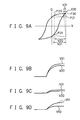
- Fig. 9D shows the potential V11 of the bit line "bl” and the potential V10 of the complementary bit line “/bl” both shown in Fig. 7.
- VBL the potential difference between the bit line “bl” and the complementary bit line “/bl”
- the potential difference VBL varies depending on the size of the parasitic capacitance CBL of the bit line “bl” and the parasitic capacitance /CBL of the complementary bit line “/bl”.
- the parasitic capacitances CBL and /CBL are substantially the same, and the ferroelectric capacitors C1 and C0 are substantially the same. It is disadvantageous for the parasitic capacitances CBL and /CBL to be excessively large as well as excessively small, since both cause the potential difference VBL to lower. This will be described with reference to Figs. 9A to 9C.
- Fig. 9A is a graphic chart showing hysteresis curves of the ferroelectric capacitors C1, C0.
- the potential difference VBL becomes small, as shown in Figs. 9B and 9C.
- the parasitic capacitances CBL, /CBL have appropriate values, the potential difference VBL becomes large as shown in Fig. 9D.
- the plate line PL is brought into high level, if the polarization Q of the ferroelectric capacitor C1 and the ferroelectric capacitor C0 is excessively small or excessively large, the potential difference VBL becomes small, as shown in Figs. 9B and 9C.
- Fig. 1 is a circuit diagram showing a configuration example of a ferroelectric memory according to a first embodiment of the present invention.
- the ferroelectric memory in Fig. 1 is configured to have a current source 110 in addition to the ferroelectric memory in Fig. 6, having the same configuration as of the ferroelectric memory in Fig. 6 except the current source 110.
- the parasitic capacitances CBL, /CBL will be omitted for the ferroelectric memory in Fig. 1, practically, the parasitic capacitances CBL, /CBL exist in the same manner as in the case of Fig. 6.
- the parasitic capacitances CBL, /CBL exist in ferroelectric memories in Fig. 2 and Fig. 4, which will be described later.
- the current source 110 is a control circuit that is connected to the bit line “bl” and the complementary bit line “/bl” so as to lower the potentials of the bit line “bl” and the complementary bit line “/bl” when the word line WL and the plate line PL is at high level. More specifically, the current source 110 lowers such potentials of the bit line “bl” and the complementary bit line “/bl” as V21, V20 shown in Fig. 9B to such appropriate potentials as V11 and V10 shown in Fig. 9D. When the potentials of the bit line “bl” and the complementary bit line “/bl” are excessively large as shown in Fig. 9B, it is possible to increase the potential difference VBL to larger as shown in Fig. 9D, by lowering the potentials of the bit line "bl” and the complementary bit line “/bl” using the current source 110.
- Fig. 2 is a circuit diagram showing a configuration example of a ferroelectric memory according to a second embodiment of the present invention, in which the ferroelectric memory is embodied in more concrete form than that of the first embodiment.
- the second embodiment is basically the same as the first embodiment, and the description below will be given for differences.
- a reference circuit 200 is additionally provided and the current source 110 is embodied in more concrete form.
- the current source 110 includes n-channel transistors Q00, Q01, Q10, Q11 and switching elements 203, 204.
- the ferroelectric memory includes a number of memory cells, allowing a number of data to be stored.
- a single memory cell includes the two transistors 103, 104 and the two ferroelectric capacitors C1, C0.
- the single reference circuit 200 is provided for a number of memory cells.
- the reference circuit 200 includes the transistors 103, 104, the ferroelectric capacitors C1, C0, a bit line RBL, a complementary bit line /RBL, and the sense amplifier 101 in the same manner as in the memory cell.
- the bit line RBL and the complementary bit line /RBL have the same configurations as of the bit line “bl” and the complementary bit line “/bl” and have parasitic capacitances CBL, /CBL, different reference numbers are used for the purpose of distinguishing them.
- the gates of the transistors 103, 104 are connected to the same word line WL, and also the plate line PL is used in common.
- the ferroelectric capacitor C1 stores fixed data "1”
- the ferroelectric capacitor C0 stores fixed data "0 (zero)".
- the ferroelectric capacitor C0 and the ferroelectric capacitor C1 store fixed data complementing each other.
- n-channel transistor QR1 As for an n-channel transistor QR1, the gate and the drain are connected to each other and the source is connected to the ground potential (reference potential) via a switching element 201. The mutual connection point of the gate and the drain is connected to the reference bit line RBL. As for an n-channel transistor QR0 (zero), the gate and the drain are connected to each other and the source is connected to the ground potential via a switching element 202. The mutual connection point of the gate and the drain is connected to the complementary reference bit line /RBL.
- the gate is connected to the reference bit line "RBL”, the drain is connected to the bit line "bl”, and the source is connected to the ground potential via the switching element 203.
- the gate is connected to the complementary reference bit line /RBL, the drain is connected to the bit line "bl”, and the source is connected to the ground potential via the switching elements 203.
- the transistor Q10 and the transistor Q11 are connected in parallel to each other.
- the gate is connected to the reference bit line RBL, the drain is connected to the complementary bit line "/bl”, and the source is connected to the ground potential via the switching elements 204.
- the gate is connected to the complementary reference bit line /RBL, the drain is connected to the complementary bit line "/bl”, the source is connected to the ground potential via the switching elements 204.
- the transistor Q01 and the transistor Q00 are connected in parallel to each other.
- the transistors QR1, Q11, and Q01 configure a current mirror circuit and the same current flows therein.
- the transistors QR0, Q10, Q00 configure a current mirror circuit and the same current flows therein.
- the reference circuit 200 is a circuit to cause the same current as of the actual memory cell to flow with the help of the current mirror circuit.
- the currents flowing in the transistors QR1, QR0 are represented by Ir1 and Ir0, and the currents flowing in the transistors Q11, Q10, Q01, Q00 are represented by I11, I10, I01, I00, respectively.
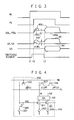
- Fig. 3 is a timing chart for illustrating an operation of the ferroelectric memory in Fig. 2.
- the word line WL and the plate line PL are at low level.
- the transistors 103, 104 are turned OFF, and the reference bit line RBL, the complementary reference bit line /RBL, the bit line “bl”, and the complementary bit line “/bl” come to 0V.
- the sense amplifier (SA) 101 is in an inactive state.
- the switching elements 201 to 204 are turned OFF (disconnected).
- the transistors 103, 104 are turned ON.
- the reference bit line RBL is connected to the ferroelectric capacitor C1
- the complementary reference bit line /RBL is connected to the ferroelectric capacitor C0
- the bit line “bl” is connected to the ferroelectric capacitor C1
- the complementary bit line “/bl” is connected to the ferroelectric capacitor C0. Since the plate line PL is at 0V, the bit lines RBL, /RBL, "bl”, “/bl” are at 0V.
- the plate line PL is brought into high level (for example to VP).
- the reference bit line RBL increases toward the potential V21, whereas it falls in due time to a threshold voltage Vth of the transistor QR1 affected by the transistor QR1.
- the complementary reference bit line /RBL increases toward the potential V21, whereas it falls in due time to the threshold voltage Vth of the transistor QR0 affected by the transistor QR0.
- the potentials Vth of the reference bit line RBL are supplied.
- the potentials Vth of the complementary reference bit line /RBL are supplied.
- the transistors Q11, Q10, Q01, Q00 serve as the current source.
- bit line “bl” increases toward the potential V21, whereas the transistors Q11 and Q10 pull out charge from the bit line “bl”, so that the potential lowers to the appropriate value.
- This appropriate value is a potential larger than 0V.
- the complementary bit line “/bl” increases toward the potential V20, whereas the transistors Q01 and Q00 pull out charge from the complementary bit line “/bl”, so that the potential lowers to the appropriate value.
- This appropriate value is a potential smaller than the potential of the bit line "bl”.
- the potential difference VBL between the bit line "bl” and the complementary bit line “/bl” becomes a larger appropriate value.
- the plate line PL is brought into low level, the sense amplifier (SA) 101 is inactivated, and the word line WL is brought into low level.
- the bit lines “bl”, “/bl” require no capacitance to be added, so that area increase and fluctuation in the potential difference VBL can be prevented.
- the parasitic capacitances of the bit lines “bl”, “/bl” it is possible to increase the potential difference VBL that is read out from the ferroelectric capacitors C1, C0 to the bit lines "bl", “/bl” in accordance with the data stored in the ferroelectric capacitors C1, C0.
- the readout data can be improved in reliability.
- stable bit-line potentials can be obtained without the need to add new capacitance.
- Fig. 4 is a circuit diagram showing a configuration example of a ferroelectric memory according to a third embodiment of the present invention, in which the ferroelectric memory is embodied in more concrete form than that of the first embodiment.
- the third embodiment is basically the same as the second embodiment, and the description below will be given for differences.
- the transistor 104, the ferroelectric capacitor C0, the complementary reference bit line /RBL, the sense amplifier 101, the transistor QR0, and the switching element 202 of the second embodiment are removed from the reference circuit 200. Further, according to the present embodiment, the transistors Q10, Q00 of the second embodiment (Fig. 2) are removed from the current source 110.
- the reference circuit 200 includes a single transistor 103 and a single ferroelectric capacitor C1, which always generate fixed data "1" as a memory cell.
- the potential of the reference bit line RBL generated in the reference circuit 200 is supplied to the gates of the transistors Q11, Q01 connected to the actual memory cell.
- Fig. 5 is a timing chart for illustrating an operation of the ferroelectric memory in Fig. 4. The description is the same as of Fig. 3 up to the time "t2".
- the reference bit line RBL increases toward the potential V21, whereas falls in due time to the threshold voltage Vth of the transistor QR1 affected by the transistor QR1.
- the potential Vth of the reference bit line RBL is supplied to the gates of the transistors Q11, Q01.
- bit line “bl” increases toward the potential V21, whereas the potential falls to the appropriate value, since the transistor Q11 pulls out charge from the bit line “bl”.
- the complementary bit line “/bl” increases toward the potential V20, whereas the potential falls to the appropriate value, since the transistor Q01 pulls out charge from the complementary bit line “/bl”.
- the potential difference VBL between the bit line “bl” and the complementary bit line “/bl” becomes a large appropriate value. Subsequent description is the same as of Fig. 3.
Landscapes
- Engineering & Computer Science (AREA)
- Computer Hardware Design (AREA)
- Power Engineering (AREA)
- Dram (AREA)
Applications Claiming Priority (2)
| Application Number | Priority Date | Filing Date | Title |
|---|---|---|---|
| JP2004159032A JP4079910B2 (ja) | 2004-05-28 | 2004-05-28 | 強誘電体メモリ |
| JP2004159032 | 2004-05-28 |
Publications (2)
| Publication Number | Publication Date |
|---|---|
| EP1600979A1 true EP1600979A1 (fr) | 2005-11-30 |
| EP1600979B1 EP1600979B1 (fr) | 2009-05-20 |
Family
ID=34927994
Family Applications (1)
| Application Number | Title | Priority Date | Filing Date |
|---|---|---|---|
| EP04030747A Expired - Lifetime EP1600979B1 (fr) | 2004-05-28 | 2004-12-24 | Mémoire ferroelectrique |
Country Status (5)
| Country | Link |
|---|---|
| US (1) | US7180765B2 (fr) |
| EP (1) | EP1600979B1 (fr) |
| JP (1) | JP4079910B2 (fr) |
| KR (1) | KR100649465B1 (fr) |
| DE (1) | DE602004021169D1 (fr) |
Cited By (1)
| Publication number | Priority date | Publication date | Assignee | Title |
|---|---|---|---|---|
| EP1688955A3 (fr) * | 2005-01-05 | 2006-09-13 | Fujitsu Limited | Dispositif de mémoire à semi-conducteur |
Families Citing this family (4)
| Publication number | Priority date | Publication date | Assignee | Title |
|---|---|---|---|---|
| JP4452631B2 (ja) | 2005-01-21 | 2010-04-21 | パトレネラ キャピタル リミテッド, エルエルシー | メモリ |
| JP4295253B2 (ja) * | 2005-07-06 | 2009-07-15 | 富士通マイクロエレクトロニクス株式会社 | 強誘電体記憶装置 |
| JP2013033566A (ja) * | 2011-08-01 | 2013-02-14 | Fujitsu Semiconductor Ltd | 半導体メモリおよびシステム |
| US20130064027A1 (en) * | 2011-09-14 | 2013-03-14 | Meng-Yi Wu | Memory and Method of Adjusting Operating Voltage thereof |
Citations (4)
| Publication number | Priority date | Publication date | Assignee | Title |
|---|---|---|---|---|
| EP0721190A2 (fr) * | 1995-01-04 | 1996-07-10 | Nec Corporation | Mémoire ferro-électrique et méthode de commande pour son opération |
| US20030026123A1 (en) * | 2000-05-10 | 2003-02-06 | Kabushiki Kaisha Toshiba | Semiconductor memory device |
| EP1304701A1 (fr) * | 2001-10-18 | 2003-04-23 | STMicroelectronics S.r.l. | Circuit de détection pour mémoires électriques ferroélectriques non volatiles |
| EP1306851A1 (fr) * | 2001-10-24 | 2003-05-02 | STMicroelectronics S.r.l. | Méthode de lecture à fatigue réduite et circuit pour des unités de mémoire ferroélectriques non volatiles |
Family Cites Families (6)
| Publication number | Priority date | Publication date | Assignee | Title |
|---|---|---|---|---|
| US5237533A (en) * | 1991-12-20 | 1993-08-17 | National Semiconductor Corporation | High speed switched sense amplifier |
| US5880989A (en) * | 1997-11-14 | 1999-03-09 | Ramtron International Corporation | Sensing methodology for a 1T/1C ferroelectric memory |
| JPH11273360A (ja) * | 1998-03-17 | 1999-10-08 | Toshiba Corp | 強誘電体記憶装置 |
| JP3866913B2 (ja) * | 2000-11-21 | 2007-01-10 | 富士通株式会社 | 半導体装置 |
| JP2003051184A (ja) * | 2001-08-06 | 2003-02-21 | Nec Corp | メモリ装置 |
| JP4099349B2 (ja) | 2002-06-04 | 2008-06-11 | 富士通株式会社 | 強誘電体メモリ |
-
2004
- 2004-05-28 JP JP2004159032A patent/JP4079910B2/ja not_active Expired - Fee Related
- 2004-12-24 EP EP04030747A patent/EP1600979B1/fr not_active Expired - Lifetime
- 2004-12-24 DE DE602004021169T patent/DE602004021169D1/de not_active Expired - Lifetime
- 2004-12-30 US US11/024,718 patent/US7180765B2/en not_active Expired - Lifetime
- 2004-12-31 KR KR1020040117611A patent/KR100649465B1/ko not_active Expired - Fee Related
Patent Citations (4)
| Publication number | Priority date | Publication date | Assignee | Title |
|---|---|---|---|---|
| EP0721190A2 (fr) * | 1995-01-04 | 1996-07-10 | Nec Corporation | Mémoire ferro-électrique et méthode de commande pour son opération |
| US20030026123A1 (en) * | 2000-05-10 | 2003-02-06 | Kabushiki Kaisha Toshiba | Semiconductor memory device |
| EP1304701A1 (fr) * | 2001-10-18 | 2003-04-23 | STMicroelectronics S.r.l. | Circuit de détection pour mémoires électriques ferroélectriques non volatiles |
| EP1306851A1 (fr) * | 2001-10-24 | 2003-05-02 | STMicroelectronics S.r.l. | Méthode de lecture à fatigue réduite et circuit pour des unités de mémoire ferroélectriques non volatiles |
Cited By (2)
| Publication number | Priority date | Publication date | Assignee | Title |
|---|---|---|---|---|
| EP1688955A3 (fr) * | 2005-01-05 | 2006-09-13 | Fujitsu Limited | Dispositif de mémoire à semi-conducteur |
| US7180766B2 (en) | 2005-01-05 | 2007-02-20 | Fujitsu Limited | Semiconductor memory |
Also Published As
| Publication number | Publication date |
|---|---|
| JP4079910B2 (ja) | 2008-04-23 |
| DE602004021169D1 (de) | 2009-07-02 |
| KR100649465B1 (ko) | 2006-11-27 |
| EP1600979B1 (fr) | 2009-05-20 |
| US7180765B2 (en) | 2007-02-20 |
| US20050265065A1 (en) | 2005-12-01 |
| KR20050113124A (ko) | 2005-12-01 |
| JP2005339704A (ja) | 2005-12-08 |
Similar Documents
| Publication | Publication Date | Title |
|---|---|---|
| KR101050699B1 (ko) | 반도체 메모리 디바이스 | |
| TW543182B (en) | Semiconductor integrated circuit | |
| US7177203B2 (en) | Data readout circuit and semiconductor device having the same | |
| US7869252B2 (en) | Ferroelectric memory device, method for driving ferroelectric memory device, and electronic equipment | |
| KR0140175B1 (ko) | 반도체 메모리 장치의 센스앰프 회로 | |
| US7729181B2 (en) | Semiconductor storage device using a bitline GND sensing scheme for a reduced real estate of pre-sense amplifier | |
| US6292418B1 (en) | Semiconductor memory device | |
| WO2007059402A2 (fr) | Circuit et procede de prereglage de canal bit pour mecanisme de detection de memoire flash | |
| US7307867B2 (en) | Over-driven access method and device for ferroelectric memory | |
| EP1600979B1 (fr) | Mémoire ferroelectrique | |
| TWI222065B (en) | Integrated circuit memory devices including active load circuits and related methods | |
| US6426906B1 (en) | Read-out circuit | |
| US6400615B2 (en) | Voltage raising circuit for semiconductor memory | |
| US7269049B2 (en) | Ferroelectric random access memory device | |
| EP1030312A2 (fr) | Mémoire ferroélectrique | |
| CN1905062B (zh) | 铁电存储装置 | |
| US20070008766A1 (en) | Ferroelectric storage device | |
| US6498743B2 (en) | Method for supplying reference potential to sense amplifier circuit in semiconductor integrated circuit, semiconductor integrated circuit, semiconductor device equipped with many of the semiconductor integrated circuits, and electronic apparatus using the semiconductor device | |
| JP4374549B2 (ja) | 強誘電体メモリ装置、電子機器および強誘電体メモリ装置の駆動方法 | |
| CN108735259A (zh) | 半导体存储装置以及半导体存储装置的读出方法 | |
| US6195281B1 (en) | Apparatus for generating reference voltage in ferroelectric memory device | |
| KR100365564B1 (ko) | 반도체 장치 | |
| US7173868B2 (en) | Sense amplifier of ferroelectric memory device | |
| KR940008139B1 (ko) | 반도체 메모리 장치의 데이타 감지 증폭회로 | |
| KR100256253B1 (ko) | 비휘발성 반도체 메모리 장치 |
Legal Events
| Date | Code | Title | Description |
|---|---|---|---|
| PUAI | Public reference made under article 153(3) epc to a published international application that has entered the european phase |
Free format text: ORIGINAL CODE: 0009012 |
|
| AK | Designated contracting states |
Kind code of ref document: A1 Designated state(s): AT BE BG CH CY CZ DE DK EE ES FI FR GB GR HU IE IS IT LI LT LU MC NL PL PT RO SE SI SK TR |
|
| AX | Request for extension of the european patent |
Extension state: AL BA HR LV MK YU |
|
| 17P | Request for examination filed |
Effective date: 20060509 |
|
| AKX | Designation fees paid |
Designated state(s): DE FR |
|
| GRAP | Despatch of communication of intention to grant a patent |
Free format text: ORIGINAL CODE: EPIDOSNIGR1 |
|
| RAP1 | Party data changed (applicant data changed or rights of an application transferred) |
Owner name: FUJITSU MICROELECTRONICS LIMITED |
|
| GRAS | Grant fee paid |
Free format text: ORIGINAL CODE: EPIDOSNIGR3 |
|
| GRAA | (expected) grant |
Free format text: ORIGINAL CODE: 0009210 |
|
| AK | Designated contracting states |
Kind code of ref document: B1 Designated state(s): DE FR |
|
| REF | Corresponds to: |
Ref document number: 602004021169 Country of ref document: DE Date of ref document: 20090702 Kind code of ref document: P |
|
| PLBE | No opposition filed within time limit |
Free format text: ORIGINAL CODE: 0009261 |
|
| STAA | Information on the status of an ep patent application or granted ep patent |
Free format text: STATUS: NO OPPOSITION FILED WITHIN TIME LIMIT |
|
| 26N | No opposition filed |
Effective date: 20100223 |
|
| PGFP | Annual fee paid to national office [announced via postgrant information from national office to epo] |
Ref country code: FR Payment date: 20091202 Year of fee payment: 6 |
|
| REG | Reference to a national code |
Ref country code: FR Ref legal event code: ST Effective date: 20110831 |
|
| PG25 | Lapsed in a contracting state [announced via postgrant information from national office to epo] |
Ref country code: FR Free format text: LAPSE BECAUSE OF NON-PAYMENT OF DUE FEES Effective date: 20110103 |
|
| PGFP | Annual fee paid to national office [announced via postgrant information from national office to epo] |
Ref country code: DE Payment date: 20191210 Year of fee payment: 16 |
|
| REG | Reference to a national code |
Ref country code: DE Ref legal event code: R119 Ref document number: 602004021169 Country of ref document: DE |
|
| PG25 | Lapsed in a contracting state [announced via postgrant information from national office to epo] |
Ref country code: DE Free format text: LAPSE BECAUSE OF NON-PAYMENT OF DUE FEES Effective date: 20210701 |