EP1601005A2 - Peeling device for chip detachment - Google Patents
Peeling device for chip detachment Download PDFInfo
- Publication number
- EP1601005A2 EP1601005A2 EP05076250A EP05076250A EP1601005A2 EP 1601005 A2 EP1601005 A2 EP 1601005A2 EP 05076250 A EP05076250 A EP 05076250A EP 05076250 A EP05076250 A EP 05076250A EP 1601005 A2 EP1601005 A2 EP 1601005A2
- Authority
- EP
- European Patent Office
- Prior art keywords
- chip
- adhesive tape
- contact surface
- raised contact
- platform
- Prior art date
- Legal status (The legal status is an assumption and is not a legal conclusion. Google has not performed a legal analysis and makes no representation as to the accuracy of the status listed.)
- Withdrawn
Links
Images

Classifications
-
- H—ELECTRICITY
- H10—SEMICONDUCTOR DEVICES; ELECTRIC SOLID-STATE DEVICES NOT OTHERWISE PROVIDED FOR
- H10P—GENERIC PROCESSES OR APPARATUS FOR THE MANUFACTURE OR TREATMENT OF DEVICES COVERED BY CLASS H10
- H10P54/00—Cutting or separating of wafers, substrates or parts of devices
-
- H—ELECTRICITY
- H10—SEMICONDUCTOR DEVICES; ELECTRIC SOLID-STATE DEVICES NOT OTHERWISE PROVIDED FOR
- H10P—GENERIC PROCESSES OR APPARATUS FOR THE MANUFACTURE OR TREATMENT OF DEVICES COVERED BY CLASS H10
- H10P72/00—Handling or holding of wafers, substrates or devices during manufacture or treatment thereof
- H10P72/04—Apparatus for manufacture or treatment
- H10P72/0442—Apparatus for placing on an insulating substrate, e.g. tape
-
- H—ELECTRICITY
- H10—SEMICONDUCTOR DEVICES; ELECTRIC SOLID-STATE DEVICES NOT OTHERWISE PROVIDED FOR
- H10W—GENERIC PACKAGES, INTERCONNECTIONS, CONNECTORS OR OTHER CONSTRUCTIONAL DETAILS OF DEVICES COVERED BY CLASS H10
- H10W72/00—Interconnections or connectors in packages
-
- Y—GENERAL TAGGING OF NEW TECHNOLOGICAL DEVELOPMENTS; GENERAL TAGGING OF CROSS-SECTIONAL TECHNOLOGIES SPANNING OVER SEVERAL SECTIONS OF THE IPC; TECHNICAL SUBJECTS COVERED BY FORMER USPC CROSS-REFERENCE ART COLLECTIONS [XRACs] AND DIGESTS
- Y10—TECHNICAL SUBJECTS COVERED BY FORMER USPC
- Y10T—TECHNICAL SUBJECTS COVERED BY FORMER US CLASSIFICATION
- Y10T156/00—Adhesive bonding and miscellaneous chemical manufacture
- Y10T156/11—Methods of delaminating, per se; i.e., separating at bonding face
- Y10T156/1168—Gripping and pulling work apart during delaminating
- Y10T156/1179—Gripping and pulling work apart during delaminating with poking during delaminating [e.g., jabbing, etc.]
-
- Y—GENERAL TAGGING OF NEW TECHNOLOGICAL DEVELOPMENTS; GENERAL TAGGING OF CROSS-SECTIONAL TECHNOLOGIES SPANNING OVER SEVERAL SECTIONS OF THE IPC; TECHNICAL SUBJECTS COVERED BY FORMER USPC CROSS-REFERENCE ART COLLECTIONS [XRACs] AND DIGESTS
- Y10—TECHNICAL SUBJECTS COVERED BY FORMER USPC
- Y10T—TECHNICAL SUBJECTS COVERED BY FORMER US CLASSIFICATION
- Y10T156/00—Adhesive bonding and miscellaneous chemical manufacture
- Y10T156/19—Delaminating means
- Y10T156/1978—Delaminating bending means
- Y10T156/1983—Poking delaminating means
Definitions
- the invention relates to the detachment of a semiconductor chip from an adhesive film or tape to which it has been mounted for processing, and in particular, to an apparatus and method for partially peeling the chip from the film or tape prior to total removal therefrom.
- the chips are typically fabricated first in the form of a wafer slice containing an array of chips. Thereafter, the chips are usually singulated in a dicing process to physically separate them from one another. Dicing is commonly carried out while the wafer is mounted onto an adhesive tape (such as Mylar film) secured by a wafer ring. After dicing, there is a need to detach each chip individually from the wafer and mount them onto a carrier such as a leadframe, printed wiring board (“PWB”) substrate or another chip during chip bonding or flip chip processes.
- a carrier such as a leadframe, printed wiring board (“PWB”) substrate or another chip during chip bonding or flip chip processes.
- the semiconductor chip detachment process is one of the key processes in electronic packaging in which each chip on a singulated wafer is picked and detached from the dicing adhesive tape for subsequent packaging.
- a popular method is to use a vacuum collet as a pick-and-place device to remove each chip from the adhesive tape and to place it on the bonding location.
- a vacuum collet As a pick-and-place device to remove each chip from the adhesive tape and to place it on the bonding location.
- a method comprising the use of an ejector assembly in conjunction with the vacuum collet is probably the most well-known for initiating the aforesaid delamination.
- an individual singulated chip is firstly aligned with a center of a supporting platform of a vacuum enclosure in which an ejector assembly is mounted for movement relative to the supporting platform and adapted to push the chips away from the adhesive tape.
- Vacuum suction is applied via a vacuum hole on the platform to hold the chip in position as well as to hold down the adhesive tape against the surface of the vacuum platform, while the ejector assembly is pushing the chip in an opposite direction.
- the ejector assembly may comprise an ejector pin, such as in US patent number 5,755,373 for a "Die Push-Up Device".
- the patent discloses a push-up needle that pushes up the chip while a wafer sheet is held in place by vacuum suction in order to facilitate separation of the chip from the wafer sheet.
- the vacuum suction provided by vacuum enclosure via holes on its platform and the mechanical force acting at the back of the chip by the push-up ejector pin induce bending moment on the chip as well as peeling stress between the interface of the chip and the plastic adhesive tape. The peeling stress at the interface will cause the delamination of the chip and the adhesive tape and hence the chip is detached from the adhesive tape.
- a problem with the use of an ejector pin such as the push-up needle described is that the surface area of the pin in contact with the chip is small and therefore the pinning effect of the pin is strong. While this method is applicable for a thick semiconductor chip (say, of a thickness greater than 0.2 mm) of smaller size (say, of a width of less than 2 mm), if thinner or larger dice are being handled, the bending moment in the chip may lead to chip crack failure.
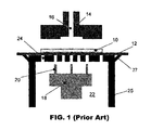
- FIG. 1 is a cross-sectional side view of a prior art chip ejector mechanism including multiple ejector pins 20 that may be utilized to reduce the distance between the pins 20 and the edges of a chip 10 being detached. It comprises a collet 14 with a vacuum channel 16 to create vacuum suction, a vacuum enclosure 25 and an ejector chuck 18 with multiple ejector pins 20.
- the top surface of the vacuum enclosure 25 of the prior art generally rests flat against a bottom surface of the adhesive tape 12 holding the chip 10.
- the ejector pins 20 are made to move up to lift the adhesive tape 12 and the chip 10 for delaminating the chip 10 from the adhesive tape 12.
- the collet 14 may pick up the chip 10 by vacuum suction.
- the push-up pins 20 cannot be too close to the edge of the chip 10 since the pinning effect will activate microcracks (which are typically introduced by dicing of a wafer) along the chip edges.
- the push-up pins located at the peripheral of the chip may inhibit the propagation of delamination into the center of a larger chip.
- US patent number 4,850,780 for a "Pre-Peel Die Ejector Apparatus” describes a two-stage process for chip separation.
- a die ejector chuck is provided with a central housing and an outer housing, and the central housing is provided with a central die eject collar which extends though an aperture in the outer housing.
- the central die eject collar is movable towards a preselected chip for detachment and away from the outer housing so as to stretch the flexible adhesive tape supporting the preselected chip, after which the chip is further separable from the adhesive tape by an ejector pin to permit the chip to be picked up with a vacuum collet.
- peeling device for detachment of a chip from an adhesive tape on which it is mounted, comprising: a platform including a first surface and a raised contact surface set at a determinate height with respect to the first surface, the raised contact surface having a width that is smaller than a width of the chip for contacting the adhesive tape at a position of the chip; and an elevation device projectable from the raised contact surface and movable with respect to the platform for lifting the chip away from the adhesive tape.
- a method of detaching a chip from an adhesive tape on which it is mounted comprising the steps of: contacting a raised contact surface of a platform against the adhesive tape at a position of the chip, wherein the raised contact surface is set at a determinate height with respect to a first surface of the platform and a width of the raised contact surface is smaller than a width of the chip; projecting an elevation device from the raised contact surface; and lifting the chip with the elevation device.
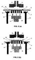
- FIG. 2 (a) is a cross-sectional side view of a peeling device in the form of a chip ejector assembly according to the preferred embodiment of the invention. It comprises a platform, which may be in the form of a vacuum enclosure 26, enclosing an elevation device such as an ejector chuck 18 and a vacuum chamber 22.
- a vacuum collet 14 having a vacuum path 16 to generate vacuum force is provided for picking up a chip 10 mounted on an adhesive tape 12.
- the ejector chuck 18 preferably has multiple ejector pins 20.
- the vacuum enclosure 26 includes a raised contact surface in the form of a stepped extrusion 28 at the central region of a first surface or top platform 30 of the said vacuum enclosure 26.
- the stepped extrusion 28 is in a relatively fixed position on the first surface or top platform 30, and moves together with the top platform 30.
- the geometry of the stepped extrusion 28 may provide a vacuum peeling mechanism to assist the detachment of the semiconductor chip 10 from the flexible plastic adhesive tape 12.
- the stepped extrusion 28 and the top platform 30 respectively provide geometrical support to the semiconductor chip 10 to be picked up and to the surrounding chips.
- a width of the stepped extrusion 28 is smaller than a width of the chip 10 so that delamination may be initiated between the portions of the adhesive tape not in contact with the stepped extrusion 28.
- both widths of the stepped extrusion 28 are smaller than the widths of the chip 10.
- Vacuum channels 24' are constructed on the top platform 30 around the stepped extrusion 28 so that the adhesive tape 12 and hence the adhered semiconductor chips 10 are held in position relative to the stepped extrusion 28 and the top platform 30 by vacuum suction. Further, vacuum channels 24 are formed in the stepped extrusion to hold the adhesive tape 12 against the stepped extrusion 28.
- the adhesive tape 12 When vacuum suction is applied to the vacuum chamber 22, the adhesive tape 12 will be held down by the vacuum suction so that it conforms to the geometries of the stepped extrusion 28 and top platform 30. This will provide a peeling effect to initiate the delamination of the interface between the adhesive tape and the respective edges of the chip 10 not supported by the stepped extrusion 28.
- Figure 2 (b) shows the effect of peeling in the interface between the semiconductor chip 10 and adhesive tape 12 induced by vacuum suction from a suction device.
- the suction device comprises vacuum channels 24' coupled to a vacuum source that are formed on the top platform 30 adjacent to the stepped extrusion 28. Delamination of this interface occurs when the adhesive tape 12 is drawn towards the top platform 30 of the vacuum enclosure 26 around the stepped extrusion 28 in the presence of vacuum suction generated via the vacuum channels 24'. Further or alternatively, the stepped extrusion 28 may be moved upwards in an additional upward stroke to lift the chip 10 and induce separation of the adhesive tape 12 from the chip 10 with or without the application of vacuum suction via the vacuum channels 24'.
- a seal ring 27 is arranged on the vacuum enclosure 26 and is preferably located along a periphery of the vacuum enclosure 26.
- the highest point of the seal ring 27 is configured to be lower than the height of the stepped extrusion 28 and may be level with the top platform 30.
- the said delamination will start from the edges and corners of the chip 10 as the adhesive tape 12 is peeled away from the chip 10, while the stepped extrusion 28 keeps a portion of the adhesive tape 12 corresponding to the centre of the chip 10 relatively flat.
- the vacuum channels 24' are specifically located in dose proximity to the straight edges of the stepped extrusion 28 on the top platform 30 to provide vacuum suction force for effective peeling.
- the ejector assembly takes advantage of a combination of mechanical parts motion and vacuum suction.
- the vacuum collet 14 descends and lands on the top surface of a semiconductor chip 10.
- vacuum suction is applied via the vacuum channels 24' on the vacuum enclosure 26.
- This vacuum suction and the straight edges of the stepped extrusion 28 initiate the delamination of interface between the adhesive tape 12 and the chip 10 at the edges and corners of the semiconductor chip 10 being picked.
- the ejector pins 20 of the ejector chuck 18 are projected from the surface of the vacuum enclosure 26, more specifically from the stepped extrusion 28. which is underneath the chip 10 and the adhesive tape 12. The position of the multiple ejector pins 20 with respect to the vertical edges of the stepped extrusion 28 then allows further delamination of the chip 10 from the adhesive tape 12 by lifting the chip 10 away from the adhesive tape 12.
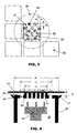
- FIG. 3 is a plan view of a plurality of chips arranged on an adhesive tape with the chip ejector assembly of FIG. 2 (a) positioned underneath a chip to be detached.
- FIG. 4 is a cross-sectional side view of the chip ejector assembly wherein the relative dimensions of the chip and chip ejector assembly are represented.
- the planar dimension of the stepped extrusion 28 is smaller than the planar dimension of the semiconductor chip 10.
- the distance between the edge of the chip and the edge of the extrusion (A 1 and A 2 in FIG. 3) is designed within a specific range.
- the said distance (A 1 and A 2 ) depends on the thickness of the chip 10 and the adhesion strength of the adhesive tape 12.
- the step height, E, of the stepped extrusion 28 is also kept within a specific value (within a range 0.1-0.66 mm for a chip with a thickness of 0.05mm-0.5mm and a width of less than 10 mm) in order to have an optimal peeling angle as well as maximum energy useable for peeling the flexible plastic adhesive tape. It also helps to provide efficient and effective formation of the vacuum suction force. Keeping the step height E within the said range further helps to keep the deformation strain or stress below the chip's critical value at a given pressure loading.
- the edges of the stepped extrusion 28 should be rounded at a radius of about 0.1 mm in order to reduce the excessive stress/strain concentration of the chip 10 at these locations.
- the height E of the stepped extrusion 28 is 0.1 ⁇ E ⁇ 0.66 mm.
- FIG. 5 is a plan view of the plurality of chips as in FIG. 3 including representations of the positions of ejector pins 20 mounted in the chip ejector assembly-
- the outer region of the chip 10 will be detached from the adhesive tape 12 when vacuum suction is applied through the vacuum channels 24' in the top platform 30 around the sides of the stepped extrusion 28.
- the ejection pins 20 will then elevate from the top surface of the stepped extrusion 28 to a pre-determined height above the stepped extrusion 28 of the vacuum enclosure 26.
- the adhesive tape will detach from the chip completely with the only contact area supported by the pins.
- the ejector pins 20 are located with a specific distance F from the edges of the stepped extrusion 28 such that F ⁇ 1 mm.
- stepped extrusion 28 and vacuum suction provides a peeling mechanism to initiate the delamination of the interface between the adhesive tape 12 and the semiconductor chip 10.
- This vacuum-assisted peeling mechanism reduces the deformation of the chip as compared to simply pushing against the chip during initial peeling and hence reduces the stress induced on the semiconductor chip so that chip cracking failure can be avoided.
- a more effective detachment mechanism is provided for detaching a semiconductor chip from an adhesive tape as compared to the prior art.
- the assembly is ideally used in a pick-up process for a semiconductor chip having planar surface areas of more than 2x2 mm 2 (but less than 10x10mm 2 ) and with thickness of less than 0.15 mm, which is mounted onto an adhesive tape 12 with an adhesion strength of less than 30 J/m 2 .
Landscapes
- Container, Conveyance, Adherence, Positioning, Of Wafer (AREA)
- Folding Of Thin Sheet-Like Materials, Special Discharging Devices, And Others (AREA)
- Die Bonding (AREA)
Abstract
Description
Claims (20)
- A peeling device for detachment of a chip from an adhesive tape on which it is mounted, comprising:a platform including a first surface and a raised contact surface set at a determinate height with respect to the first surface, the raised contact surface having a width that is smaller than a width of the chip for contacting the adhesive tape at a position of the chip; andan elevation device projectable from the raised contact surface and movable with respect to the platform for lifting the chip away from the adhesive tape.
- The peeling device as claimed in claim 1, including a suction device coupled to the first surface for drawing a portion of the adhesive tape not in contact with the raised contact surface towards the platform.
- The peeling device as claimed in claim 2, wherein the suction device comprises vacuum channels coupled to a vacuum source that are formed on the first surface adjacent to the raised contact surface.
- The peeling device as claimed in claim 2 or claim 3, including a seal ring arranged on the platform that is adapted to enclose an area of the adhesive tape that is drawn towards the platform.
- The peeling device as claimed in claim 4, wherein the seal ring is located along a periphery of the platform.
- The peeling device as claimed in claim 4 or claim 5, wherein a highest point of the seal ring is configured to be lower than the height of the raised contact surface.
- The peeling device as claimed in any one of the preceding claims, including vacuum channels formed in the raised contact surface that are coupled to a vacuum source.
- The peeling device as claimed in any one of the preceding claims, including a collet that is positionable over the chip for supporting the chip during separation of the adhesive tape from the chip.
- The peeling device as claimed in any one of the preceding claims, wherein the height of the raised contact surface is between 0.1 mm to 0.66mm and the width of the chip is less than 10mm.
- The peeling device as claimed in any one of the preceding claims, wherein an edge of the raised contact surface is rounded to a radius of about 0.1mm.
- The peeling device as claimed in any one of the preceding claims, wherein the width of the raised contact surface is between 1mm to 10mm and the distance between the edge of the raised contact surface to an unsupported edge of the chip is between 0.3mm to 2mm.
- The peeling device as claimed in any one of the preceding claims, wherein the difference between the width of the raised contact surface and the width of the platform is less than 10mm.
- The peeling device as claimed in any one of the preceding claims, wherein the elevation device comprises one or more push-up pins.
- The peeling device as claimed in claim 13, wherein at least one of a plurality of push-up pins is arranged such that the distance of the push-up pin of the elevation device from an edge of the chip is less than 1 mm.
- Method of detaching a chip from an adhesive tape on which it is mounted, comprising the steps of:contacting a raised contact surface of a platform against the adhesive tape at a position of the chip, wherein the raised contact surface is set at a determinate height with respect to a first surface of the platform and a width of the raised contact surface is smaller than a width of the chip;projecting an elevation device from the raised contact surface; andlifting the chip with the elevation device.
- Method as claimed in claim 15, including the step of drawing a portion of the adhesive tape around the raised contact surface that is not contacted by the raised contact surface away from the chip prior to lifting the chip with the elevation device.
- Method as claimed in claim 16, including enclosing an area of the adhesive tape drawn away from the chip with a seal ring arranged on the platform.
- Method as claimed in claim 16 or claim 17, wherein the adhesive tape is drawn away and separated from the chip using vacuum suction.
- Method as claimed in claim 18, induding the steps of forming vacuum channels in the first surface adjacent to the raised contact surface, and coupling the vacuum channels to a vacuum suction to create a vacuum suction force at the vacuum channels.
- Method as claimed in any one of claims 15 to 19, including the step of positioning a collet over the chip for supporting the chip during separation of the adhesive tape from the chip.
Applications Claiming Priority (2)
| Application Number | Priority Date | Filing Date | Title |
|---|---|---|---|
| US857067 | 2004-05-28 | ||
| US10/857,067 US20050274457A1 (en) | 2004-05-28 | 2004-05-28 | Peeling device for chip detachment |
Publications (2)
| Publication Number | Publication Date |
|---|---|
| EP1601005A2 true EP1601005A2 (en) | 2005-11-30 |
| EP1601005A3 EP1601005A3 (en) | 2008-11-12 |
Family
ID=34938309
Family Applications (1)
| Application Number | Title | Priority Date | Filing Date |
|---|---|---|---|
| EP05076250A Withdrawn EP1601005A3 (en) | 2004-05-28 | 2005-05-27 | Peeling device for chip detachment |
Country Status (7)
| Country | Link |
|---|---|
| US (1) | US20050274457A1 (en) |
| EP (1) | EP1601005A3 (en) |
| JP (1) | JP2005340839A (en) |
| KR (1) | KR20060046237A (en) |
| CN (1) | CN100377296C (en) |
| SG (2) | SG137865A1 (en) |
| TW (1) | TWI257651B (en) |
Cited By (2)
| Publication number | Priority date | Publication date | Assignee | Title |
|---|---|---|---|---|
| DE102006025361A1 (en) * | 2006-05-31 | 2007-12-06 | Siemens Ag | Ejection unit for separating components from a substantially planar arrangement of components |
| CN113594079A (en) * | 2020-04-30 | 2021-11-02 | 先进科技新加坡有限公司 | Ejector unit for separating electronic component from adhesive carrier |
Families Citing this family (30)
| Publication number | Priority date | Publication date | Assignee | Title |
|---|---|---|---|---|
| EP1587138B1 (en) * | 2004-04-13 | 2007-05-30 | Oerlikon Assembly Equipment AG, Steinhausen | Apparatus for mounting of semi-conductor chips and method for stripping of a semi-conductor chip from a film |
| KR100582056B1 (en) * | 2004-07-05 | 2006-05-23 | 삼성전자주식회사 | Thin chip separating device and thin chip separating method using same |
| US7276396B2 (en) * | 2004-10-06 | 2007-10-02 | Intel Corporation | Die handling system |
| JP4624813B2 (en) | 2005-01-21 | 2011-02-02 | ルネサスエレクトロニクス株式会社 | Semiconductor device manufacturing method and semiconductor manufacturing apparatus |
| US7238258B2 (en) * | 2005-04-22 | 2007-07-03 | Stats Chippac Ltd. | System for peeling semiconductor chips from tape |
| JP4607748B2 (en) * | 2005-12-02 | 2011-01-05 | 東京エレクトロン株式会社 | Substrate particle removal method, apparatus and coating and developing apparatus |
| KR20070120319A (en) * | 2006-06-19 | 2007-12-24 | 삼성전자주식회사 | Disclosed is a semiconductor chip detachment device having a pair of ejectors and a method of detaching and attaching a semiconductor chip using the same |
| JP4693805B2 (en) * | 2007-03-16 | 2011-06-01 | 株式会社東芝 | Semiconductor device manufacturing apparatus and manufacturing method |
| JP5356061B2 (en) * | 2009-02-18 | 2013-12-04 | キヤノンマシナリー株式会社 | Peeling apparatus and peeling method |
| US8141612B2 (en) * | 2009-04-02 | 2012-03-27 | Asm Assembly Automation Ltd | Device for thin die detachment and pick-up |
| CN102044404B (en) * | 2009-10-12 | 2015-12-09 | 桑迪士克科技公司 | To tape the system be separated for making semiconductor die and nude film through cutting |
| CN102934217A (en) * | 2009-12-23 | 2013-02-13 | 休斯微技术光刻有限公司 | Automated thermal slide debonder |
| WO2012116482A1 (en) * | 2011-02-28 | 2012-09-07 | Sandisk Semiconductor (Shanghai) Co., Ltd. | Non-uniform vacuum profile die attach tip |
| FR2986175A1 (en) * | 2012-01-31 | 2013-08-02 | St Microelectronics Tours Sas | METHOD AND DEVICE FOR CUTTING A WAFER |
| JP5687647B2 (en) * | 2012-03-14 | 2015-03-18 | 株式会社東芝 | Semiconductor device manufacturing method and semiconductor manufacturing apparatus |
| US8916419B2 (en) * | 2012-03-29 | 2014-12-23 | Taiwan Semiconductor Manufacturing Company, Ltd. | Lid attach process and apparatus for fabrication of semiconductor packages |
| TWI485786B (en) * | 2012-04-16 | 2015-05-21 | Gallant Micro Machining Co Ltd | Grain Stripping Method and Device |
| CN104838483B (en) * | 2012-12-17 | 2019-05-21 | 新加坡科技研究局 | Wafer dicing device and wafer dicing method |
| TWI497631B (en) * | 2012-12-17 | 2015-08-21 | Hon Soon Internat Technology Co Ltd | Chip ejection device |
| CN104002542A (en) * | 2013-02-22 | 2014-08-27 | 深圳富泰宏精密工业有限公司 | Material ejecting device |
| CN104724336B (en) * | 2013-12-19 | 2017-01-04 | 福士瑞精密工业(晋城)有限公司 | Cutting agency |
| KR102247033B1 (en) | 2014-04-16 | 2021-05-03 | 삼성전자주식회사 | Die bonding apparatus |
| DE102016108880A1 (en) * | 2016-05-13 | 2017-11-16 | Joachim Jakob | hybrid Etter |
| CN107785298B (en) * | 2016-08-25 | 2021-02-02 | 苏州能讯高能半导体有限公司 | Separation equipment and method for wafer temporary bonding |
| CN107680910A (en) * | 2017-09-14 | 2018-02-09 | 江苏长电科技股份有限公司 | A kind of method and device for removing Burr removal |
| JP6935306B2 (en) * | 2017-11-16 | 2021-09-15 | 芝浦メカトロニクス株式会社 | Film deposition equipment |
| US11062923B2 (en) * | 2018-09-28 | 2021-07-13 | Rohinni, LLC | Apparatus to control transfer parameters during transfer of semiconductor devices |
| JP7237655B2 (en) * | 2019-03-01 | 2023-03-13 | ファスフォードテクノロジ株式会社 | Semiconductor manufacturing equipment and semiconductor device manufacturing method |
| US11282722B2 (en) * | 2019-08-23 | 2022-03-22 | YunJun Tang | Chip front surface touchless pick and place tool or flip chip bonder |
| KR102792628B1 (en) * | 2020-11-03 | 2025-04-07 | 세메스 주식회사 | Apparatus for transferring die and method thereof |
Family Cites Families (12)
| Publication number | Priority date | Publication date | Assignee | Title |
|---|---|---|---|---|
| US4850780A (en) * | 1987-09-28 | 1989-07-25 | Kulicke And Soffa Industries Inc. | Pre-peel die ejector apparatus |
| JPH0278244A (en) * | 1988-09-14 | 1990-03-19 | Hitachi Ltd | Semiconductor pellet extraction device |
| JPH03161999A (en) * | 1989-11-20 | 1991-07-11 | Sanyo Electric Co Ltd | Pushing-up equipment for electronic component |
| JPH0837395A (en) * | 1994-07-21 | 1996-02-06 | Matsushita Electric Ind Co Ltd | Semiconductor chip supply device and supply method |
| JP3079502B2 (en) * | 1995-08-18 | 2000-08-21 | 株式会社新川 | Die push-up device |
| JP3498877B2 (en) * | 1995-12-05 | 2004-02-23 | 株式会社東芝 | Semiconductor manufacturing apparatus and semiconductor device manufacturing method |
| JPH10199961A (en) * | 1997-01-14 | 1998-07-31 | Sony Corp | Chip peeling device and chip peeling method |
| JP2002050670A (en) * | 2000-08-04 | 2002-02-15 | Toshiba Corp | Pickup device and pickup method |
| JP4021614B2 (en) * | 2000-12-11 | 2007-12-12 | 株式会社東芝 | Semiconductor element pickup jig, semiconductor element pickup device, semiconductor element pickup method, semiconductor device manufacturing method, and semiconductor device manufacturing apparatus |
| JP3976541B2 (en) * | 2001-10-23 | 2007-09-19 | 富士通株式会社 | Semiconductor chip peeling method and apparatus |
| JP3870803B2 (en) * | 2002-01-09 | 2007-01-24 | 株式会社村田製作所 | Chip component supply device |
| US7238258B2 (en) * | 2005-04-22 | 2007-07-03 | Stats Chippac Ltd. | System for peeling semiconductor chips from tape |
-
2004
- 2004-05-28 US US10/857,067 patent/US20050274457A1/en not_active Abandoned
-
2005
- 2005-05-20 TW TW094116385A patent/TWI257651B/en not_active IP Right Cessation
- 2005-05-25 CN CNB2005100718573A patent/CN100377296C/en not_active Expired - Fee Related
- 2005-05-26 SG SG200718093-8A patent/SG137865A1/en unknown
- 2005-05-26 SG SG200503329A patent/SG117606A1/en unknown
- 2005-05-27 KR KR1020050045183A patent/KR20060046237A/en not_active Ceased
- 2005-05-27 EP EP05076250A patent/EP1601005A3/en not_active Withdrawn
- 2005-05-30 JP JP2005157963A patent/JP2005340839A/en active Pending
Cited By (3)
| Publication number | Priority date | Publication date | Assignee | Title |
|---|---|---|---|---|
| DE102006025361A1 (en) * | 2006-05-31 | 2007-12-06 | Siemens Ag | Ejection unit for separating components from a substantially planar arrangement of components |
| CN113594079A (en) * | 2020-04-30 | 2021-11-02 | 先进科技新加坡有限公司 | Ejector unit for separating electronic component from adhesive carrier |
| CN113594079B (en) * | 2020-04-30 | 2024-01-16 | 先进科技新加坡有限公司 | Ejector unit for separating electronic components from adhesive carriers |
Also Published As
| Publication number | Publication date |
|---|---|
| EP1601005A3 (en) | 2008-11-12 |
| TWI257651B (en) | 2006-07-01 |
| SG137865A1 (en) | 2007-12-28 |
| CN1707750A (en) | 2005-12-14 |
| SG117606A1 (en) | 2005-12-29 |
| JP2005340839A (en) | 2005-12-08 |
| US20050274457A1 (en) | 2005-12-15 |
| TW200539302A (en) | 2005-12-01 |
| CN100377296C (en) | 2008-03-26 |
| KR20060046237A (en) | 2006-05-17 |
Similar Documents
| Publication | Publication Date | Title |
|---|---|---|
| US20050274457A1 (en) | Peeling device for chip detachment | |
| US8026126B2 (en) | Apparatus and method for thin die detachment | |
| US8141612B2 (en) | Device for thin die detachment and pick-up | |
| KR100701814B1 (en) | Method and apparatus for semiconductor chip separation | |
| KR100766512B1 (en) | Method and device of peeling semiconductor device | |
| US8470130B2 (en) | Universal die detachment apparatus | |
| US7665204B2 (en) | Die detachment apparatus comprising pre-peeling structure | |
| JP2003133395A (en) | Jig for semiconductor substrate and method of manufacturing semiconductor device using the same | |
| CN100578749C (en) | Chip pickup device, chip pickup method, chip peeling device, and chip peeling method | |
| JP2006191144A (en) | Pickup device and pickup method | |
| CN113774320B (en) | Film forming device and parts peeling device | |
| JP2014239090A (en) | Pickup system | |
| JP3667241B2 (en) | Bonding method and apparatus | |
| JP5075769B2 (en) | Semiconductor chip pickup device and semiconductor chip pickup method using the same | |
| JP4613838B2 (en) | Chip pickup device and chip pickup method | |
| WO2010052760A1 (en) | Chip peeling method, semiconductor device manufacturing method and chip peeling apparatus | |
| KR100688587B1 (en) | Device for separating semiconductor chip and method for separating semiconductor chip | |
| KR20090009973U (en) | Equipment of transfering frame for fabricating semiconductor package |
Legal Events
| Date | Code | Title | Description |
|---|---|---|---|
| PUAI | Public reference made under article 153(3) epc to a published international application that has entered the european phase |
Free format text: ORIGINAL CODE: 0009012 |
|
| AK | Designated contracting states |
Kind code of ref document: A2 Designated state(s): AT BE BG CH CY CZ DE DK EE ES FI FR GB GR HU IE IS IT LI LT LU MC NL PL PT RO SE SI SK TR |
|
| AX | Request for extension of the european patent |
Extension state: AL BA HR LV MK YU |
|
| RAP1 | Party data changed (applicant data changed or rights of an application transferred) |
Owner name: ASM ASSEMBLY AUTOMATION LTD. |
|
| RIN1 | Information on inventor provided before grant (corrected) |
Inventor name: YIU, CHING HONG Inventor name: CHONG, CHI MING Inventor name: CHEUNG, YIU MING |
|
| PUAL | Search report despatched |
Free format text: ORIGINAL CODE: 0009013 |
|
| AK | Designated contracting states |
Kind code of ref document: A3 Designated state(s): AT BE BG CH CY CZ DE DK EE ES FI FR GB GR HU IE IS IT LI LT LU MC NL PL PT RO SE SI SK TR |
|
| AX | Request for extension of the european patent |
Extension state: AL BA HR LV MK YU |
|
| STAA | Information on the status of an ep patent application or granted ep patent |
Free format text: STATUS: THE APPLICATION IS DEEMED TO BE WITHDRAWN |
|
| 18D | Application deemed to be withdrawn |
Effective date: 20081202 |