EP1601015B9 - Kühlkörper für Leistungskomponenten - Google Patents
Kühlkörper für Leistungskomponenten Download PDFInfo
- Publication number
- EP1601015B9 EP1601015B9 EP05011633A EP05011633A EP1601015B9 EP 1601015 B9 EP1601015 B9 EP 1601015B9 EP 05011633 A EP05011633 A EP 05011633A EP 05011633 A EP05011633 A EP 05011633A EP 1601015 B9 EP1601015 B9 EP 1601015B9
- Authority
- EP
- European Patent Office
- Prior art keywords
- heatsink
- radio frequency
- frequency generator
- hollow portion
- coolant
- Prior art date
- Legal status (The legal status is an assumption and is not a legal conclusion. Google has not performed a legal analysis and makes no representation as to the accuracy of the status listed.)
- Expired - Lifetime
Links
Images



Classifications
-
- H—ELECTRICITY
- H10—SEMICONDUCTOR DEVICES; ELECTRIC SOLID-STATE DEVICES NOT OTHERWISE PROVIDED FOR
- H10W—GENERIC PACKAGES, INTERCONNECTIONS, CONNECTORS OR OTHER CONSTRUCTIONAL DETAILS OF DEVICES COVERED BY CLASS H10
- H10W40/00—Arrangements for thermal protection or thermal control
- H10W40/40—Arrangements for thermal protection or thermal control involving heat exchange by flowing fluids
- H10W40/47—Arrangements for thermal protection or thermal control involving heat exchange by flowing fluids by flowing liquids, e.g. forced water cooling
-
- H—ELECTRICITY
- H02—GENERATION; CONVERSION OR DISTRIBUTION OF ELECTRIC POWER
- H02M—APPARATUS FOR CONVERSION BETWEEN AC AND AC, BETWEEN AC AND DC, OR BETWEEN DC AND DC, AND FOR USE WITH MAINS OR SIMILAR POWER SUPPLY SYSTEMS; CONVERSION OF DC OR AC INPUT POWER INTO SURGE OUTPUT POWER; CONTROL OR REGULATION THEREOF
- H02M7/00—Conversion of AC power input into DC power output; Conversion of DC power input into AC power output
- H02M7/42—Conversion of DC power input into AC power output without possibility of reversal
- H02M7/44—Conversion of DC power input into AC power output without possibility of reversal by static converters
- H02M7/48—Conversion of DC power input into AC power output without possibility of reversal by static converters using discharge tubes with control electrode or semiconductor devices with control electrode
- H02M7/53—Conversion of DC power input into AC power output without possibility of reversal by static converters using discharge tubes with control electrode or semiconductor devices with control electrode using devices of a triode or transistor type requiring continuous application of a control signal
- H02M7/537—Conversion of DC power input into AC power output without possibility of reversal by static converters using discharge tubes with control electrode or semiconductor devices with control electrode using devices of a triode or transistor type requiring continuous application of a control signal using semiconductor devices only, e.g. single switched pulse inverters
- H02M7/5387—Conversion of DC power input into AC power output without possibility of reversal by static converters using discharge tubes with control electrode or semiconductor devices with control electrode using devices of a triode or transistor type requiring continuous application of a control signal using semiconductor devices only, e.g. single switched pulse inverters in a bridge configuration
-
- H—ELECTRICITY
- H05—ELECTRIC TECHNIQUES NOT OTHERWISE PROVIDED FOR
- H05K—PRINTED CIRCUITS; CASINGS OR CONSTRUCTIONAL DETAILS OF ELECTRIC APPARATUS; MANUFACTURE OF ASSEMBLAGES OF ELECTRICAL COMPONENTS
- H05K7/00—Constructional details common to different types of electric apparatus
- H05K7/20—Modifications to facilitate cooling, ventilating, or heating
- H05K7/2089—Modifications to facilitate cooling, ventilating, or heating for power electronics, e.g. for inverters for controlling motor
- H05K7/20927—Liquid coolant without phase change
Definitions
- the present invention relates to a radio frequency generator with a heatsink and related components thereof.
- thermal management is important--especially at high power generation levels which increase the amount of heat created. Heat decreases the performance and operating life of the transistor. Moreover, heat generated at the collector base junction in bipolar devices can create a temperature buildup which may eventually cause the device to short-circuit. MOSFET switching losses and channel conduction losses cause the device to overheat and may result in failure.
- the power device is generally mounted on a thermally conductive pad which acts as a heatsink and dissipates the heat generated by the power device.
- a copper plate is commonly used as a heatsink due to its good heat conductivity.
- US 2001/0 004 312 A1 discloses a semiconductor laser stack apparatus having a cooling device comprising a plurality of heatsinks wherein each heatsink has a planar structure.
- the upper planar member and the lower planar member each comprise a depression.
- a middle planar member is arranged between the upper planar member and the lower planar member.
- a liquid can flow through a depression of one of the upper and lower planar members, flow through openings of the middle planar member and into the depression of the other of the upper planar member and the lower planar member in order to cool the laser device.
- a heatsink for a power device comprises an upper plate providing a first surface; a lower plate providing a second surface; a middle plate provided between the upper and lower plates, the middle plate having a hollow portion and a solid portion, the hollow portion defining an area to receive coolant, wherein the power device is provided on the first or second surface, so that heat generated by the power device can be transferred to the coolant.
- the heatsink further comprises an input port coupled to the hollow portion of the middle plate to provide the coolant into the hollow portion; and an output port coupled to the hollow portion of the middle plate to remove the coolant from the hollow portion.
- a ratio of areas defined by the hollow portion and the solid portion is at least 2:1, so that an increased portion of the coolant can contact the upper and lower plates and more effectively transfer the heat generated by the power device to the coolant.
- the heatsink is configured to enable use of blind fasteners to mount a device on at least one of the first and second surfaces.
- a heatsink for a power device includes an upper conductive plate providing a first surface; a lower conductive plate providing a second surface; a middle conductive plate provided between the upper and lower plates, the middle plate having a hollow portion and a solid portion, the hollow portion defining an area to receive coolant, wherein the power device is provided on the first or second surface, so that heat generated by the power device can be transferred to the coolant
- Fig. 1 illustrates an RF generator coupled to an AC power source and a load.
- Fig. 2 illustrates a more detailed view of the RF generator according to one embodiment of the present invention.
- Fig. 3 illustrates an RF generator having a full bridge configuration according to one embodiment of the present invention.
- Fig. 4 illustrates at least one blocking capacitor is provided between the positive rail and the load.
- Fig. 5A illustrates the waveforms when the half bridges are controlled to output full power.
- Fig. 5B illustrates the waveforms when the MOSFETs are operated at about 90 degrees out of phase.
- Fig. 5C illustrates the waveforms when the MOSFETs are operated at 180 degrees out of phase.
- Fig. 6 illustrates a heatsink that is attached to an RF generator.
- Fig. 7 illustrates a cross-sectional view of the heatsink.
- Fig. 8 illustrates holes that do not provide a uniform distance between the coolant and the RF generator.
- Fig. 9 illustrates a heatsink having three layers (or plates) according to one embodiment of the present invention.
- Fig. 10A illustrates an exemplary second layer (or middle plate) according to one embodiment of the present invention.
- Fig. 10B illustrates a coolant passage that provides a uniform distance between the coolant and the top or bottom plates.
- Fig. 10C illustrates a middle plate according to another embodiment of the present invention.
- Fig. 11 illustrates a middle plate according to yet another embodiment of the present invention.
- the present invention relates to a power device and related components thereof.
- One type of power devices is a radio frequency (RF) generator.
- the RF generator generates a great deal of heat that needs to be dissipated effectively. Accordingly, a heatsink is commonly attached to the RF generator to dissipate heat.
- FIG. 1 illustrates an RF generator 102 coupled to an AC power source 104 and a load 106.
- the power source is a typical AC source with a relatively low frequency, e.g., 60 Hz.
- the load is a electronic device or equipment, e.g., a plasma chamber, that is operated using the RF output generated by the RF generator.
- Fig. 2 illustrates a more detailed view of the RF generator 102 according to one embodiment of the present invention.
- the RF generator includes a rectifier 202 that receives the AC current and converts it into a DC current.
- the RF generator uses fixed DC voltages rather than variable DC power supply since phase shift technique is used.
- the rectifier includes a bridge configuration to convert the 60 Hz input a DC current.
- a phase shift RF power section 204 receives the DC current and sends out an RF output according to the controls of a phase control 206.
- the phase control comprises four gate drivers, each driving a power MOSFET (see Fig. 3 ).
- the MOSFETs are arranged in a full-bridge configuration.
- Fig. 3 illustrates an RF generator 502 having a full bridge configuration according to one embodiment of the present invention.
- the RF generator 502 includes first, second, third and fourth MOSFETs 504,506,508, and 510.
- the MOSFETs are "IXYS-RF MOSFET IXZ211N50," manufactured by IXYS Corporation, but other types of power MOSFETs may be used in other implementations.
- the first and third MOSFETs 504 and 508 define a first half bridge
- the second and fourth MOSFETs 506 and 510 define a second half bridge.
- First, second, third, and fourth gate drivers 512, 514, 516, and 518, together comprising the phase control 206, are coupled to the control terminals of the first, second, third, and fourth MOSFETs, respectively.
- An AC power source 520 is coupled to a positive rail 522 and a negative rail 524 via a rectifier 521, defining a given potential difference V.
- the rectifier is provided between the AC power source and nodes 526 and 528 to provide DC currents to the node 526.
- the DC currents are supplied to the first and second MOSFETs via the positive rail 522.
- a first capacitor C1 is provided between the positive and negative rails. In the present embodiment, a fixed DC voltage is provided to the first and second MOSFETs.
- a resonant circuit 530 is provided between the output nodes of the first and second MOSFETs, so that the RF generator can operate at resonate frequency and avoid hard switching.
- the circuit 530 includes second and third capacitors C2 and C3, and first, second, and third inductors L1, L2, and L3.
- the second and third capacitors have capacitance of 5.1 nF each.
- the first and second inductors L1 and L2 have inductance of 400 nH each.
- the third inductor L3 has inductance of 40 nH. In other implementations, these components may have different values.
- the values of the inductors L1 and L2 have been selected to facilitate the commutation of the MOSFETs, such that hard switching is avoided for much of the phase shift range. Hard switching cannot be completely avoided in the present embodiment because the currents in the inductors are not identical as phase shift is varied. One of the half bridges would have a reduced current as the phase is changed from zero of 180 degrees. The reduction in current results in only a partial resonant commutation with the remainder being hard switching.
- An impedance matching circuit 532 is provided between the resonate circuit 530 and a load 534,
- the load is represented as a resistor R5.
- the matching circuit includes a fourth inductor L4 and fifth and sixth capacitors C5 and C6.
- the fourth inductor has inductance of 270 nH.
- the fifth and sixth capacitors C5 and C6 have capacitance of 180 pf and 1.1 nF, respectively. These components may have different values in different implementations.
- the RF generator 502 also includes a plurality of blocking capacitors C2, C3, and C4 to isolate the load 534 from the power section and operate the RF generator directly off line.
- the blocking capacitor or fourth capacitor C4 has capacitance of 5.1 nF in the present implementation, but may have other values in other implementations.
- At least two blocking capacitors are used. That is, at least one blocking capacitor 542 is provided between the positive rail 522 and the load 534, as shown in Fig. 4 .
- the capacitor 542 corresponds to the blocking capacitor C2 or C3.
- At least another blocking capacitor 544 is provided between the negative rail 544 and the load 534.
- the capacitor 544 corresponds to the blocking capacitor C4.
- the great difference in frequency between the high output frequency (e.g., 13.56 MHz) and the low input frequency (e.g., 60 Hz) of the AC power source 520 enables the use of low frequency blocking capacitors C2, C3, and C4 to isolate the load from the power section. This allows the output to be grounded without excessive current flow from the 60 Hz power.
- the phase of the two half bridges of the RF generator 502 is varied to control the power output.
- the output of the two half bridges are combined using a network to sum the outputs into a single node 537.
- the single node is then impedance matched to the output using the matching circuit 532.
- Figs. 5A-5C illustrate the waveforms generated by the RF generator 502 according to the present embodiment. These waveforms are illustrated as quasi-square waves for illustrative convenience. However, they are in reality closer to sine waves due to the filtering of the total network.
- Fig. 5A illustrates the waveforms when the half bridges are controlled to output full power. A zero degree phase relationship is maintained for this operation.
- a first waveform 702 illustrates the output of the MOSFET 504, and a second waveform 704 illustrates the output of the MOSFET 508.
- a third waveform 706 illustrates the output of the MOSFET 506, and a fourth waveform 708 illustrates the output of the MOSFET 510.
- An output waveform 710 illustrates the power output of the RF generator that results from combining the outputs of the above MOSFETs. Since the MOSFETs are operated in phase, full power is output.
- the node 537 switches at full pulse widths similar to the drive waveforms.
- Fig. 5B illustrates the waveforms when the MOSFETs are operated at about 90 degrees out of phase.
- a first waveform 712 illustrates the output of the MOSFET 504, and a second waveform 714 illustrates the output of the MOSFET 508.
- a third waveform 716 illustrates the output of the MOSFET 506, and a fourth waveform 718 illustrates the output of the MOSFET 510.
- An output waveform 720 illustrates the output of the RF generator that results from combining the outputs of the above MOSFETs. The power output is lower since the MOSFETs are not being operated in phase, as shown by the smaller pulses.
- Fig. 5C illustrates the waveforms when the MOSFETs are operated at 180 degrees out of phase.
- a first waveform 722 illustrates the output of the MOSFET 504, and a second waveform 724 illustrates the output of the MOSFET 508.
- a third waveform 726 illustrates the output of the MOSFET 506, and a fourth waveform 728 illustrates the output of the MOSFET 510.
- An output waveform 730 illustrates the output of the RF generator that results from combining the outputs of the above MOSFETs. Since the MOSFETs are operated 180 degrees out of phase, no power is output.
- the MOSFETs Although there is no power output when the MOSFETs are operated in 180 degrees out of phase, currents continue to flow through the inductors L1 and L2. These inductors are being charged and discharged. The potential of the node 537, however, does not change and remains at the same level. This is so since the inductors L1 and L2 are a voltage divider, each with the same inductance. The node 537 remains at V/2 (i.e., a half of the potential difference between the positive and negative rails 522 an 524) as long as the drive is symmetrical.
- the RF generator 502 handles a great deal of energy. As a result, it is generally attached to a large heatsink to effectively dissipate the heat generated by the RF generator.
- a heatsink comprises a conductive substrate, e.g., copper plate. The heatsink is attached to one side of the RF generator to dissipate the heat generated by the RF generator.
- Fig. 6 illustrates a heatsink 802 that is attached to an RF generator 804.
- Fig. 7 illustrates a cross-sectional view of the heatsink 802.
- the heatsink or heat dissipater has a length L1 that is 18 inches and a width WI that is 10 inches.
- the heatsink uses liquid coolant, e.g., water, to dissipate heat more effectively.
- the heatsink includes a plurality of vertical holes (or passages) 812 and 814 and at least one horizontal hole (or passage) 816.
- the horizontal hole connects to the vertical holes to provide a path for the coolant, so that the coolant can be input to and output from the heatsink.
- the above holes are formed by drilling into metal plate, which has a number of disadvantages. (1) It is time consuming to form the holes by drilling. (2) Since it is relatively time consuming to drill holes into the metal plate, a limited number of holes are formed. This degrades the cooling efficiency of the heatsink. (3) The holes do not provide a uniform distance between the coolant and the RF generator (see Fig. 8 ). One point 822 of the hole can be substantially further than another point 824 of the hole. This results in non-uniform heat dissipation. (4) A relatively thick metal plate is needed since holes are to be drilled into it. For example, the heatsink 802 has a thickness of about 0.5 inch. This increases the weight and material cost of the heatsink.
- Another method of making a heatsink is machining two plates and assemble them together.
- the plates are sealed by soldering, brazing or using o-ring seals.
- These plates are usually made out of copper for corrosion resistance and good thermal conductivity. Machining, however, is even more time consuming and expensive approach than the drilling.
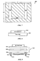
- Fig. 9 illustrates a heatsink 902 having three layers (or plates) according to one embodiment of the present invention.
- a first layer 904 is a top plate.
- a second layer 906 is a middle plate.
- a third layer 908 is a bottom plate.
- the first, second, and third layers have thicknesses of 0.125 inch, 0.1875 inch, and 0.125 inch, respectively.
- the middle plate is thicker than the top or bottom plates in the present implementation.
- the RF generator 502 is provided on one side of the heatsink, e.g., the top plate.
- Another power device or component 503 is provided on another side of the heat sink, e.g., the bottom plate.
- these layers or plates When bonded together, these layers or plates have a thickness of 0.4375 inch, which is 12.5% thinner than the conventional heatsink 802.
- the plates of the heatsink 902 are made of copper in the present invention. Other types of conductive material may be used in other applications.
- a first port 910 (or input port) is provided on one side of the bottom plate to input liquid coolant into the heatsink.
- a first hole 912 provided on the first port receives the coolant.
- a second port 914 (or output port) is provided on another side of the bottom plate.
- a second hole 916 outputs the coolant that has been input via the first hole.
- the heatsink is made by using a punched plate. This enables the heatsink to be made more quickly at lower cost.
- the middle plate is patterned by punching out the unwanted portions, thereby defining a hollow area that is configured to receive the coolant.
- the top and bottom plates are bonded to the punched middle plate. As a result, a heatsink having a coolant passage or area is formed.
- the plates may be bonded or sealed using various techniques, e.g., by soldering or brazing.
- the unwanted portions of the middle plates may removed using techniques other than punching, e.g., a torch to cut out the unwanted portions.
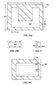
- Fig. 10A illustrates an exemplary second layer (or middle plate) 922 according to one embodiment of the present invention.
- the middle plate has a length L2 of about 18 inches and a width W2 of about 10 inches.
- Passage 924 for liquid coolant has been defined on the middle plate by punching out a portion of the middle plate. Since the passages 924 are defined by punching out the unwanted portions of the middle plate, the middle plate can be patterned very quickly and easily when compared to the drilling or machining approach.
- the width W3, L3 of the paths can be made to be quite large to carry more coolant.
- the width W3, L3 may be 2 inches, 3 inches, 4 inches, 5 inches, 6 inches, or 7 inches or more.
- the coolant path 924 is defined to be provided immediately below where the RF generator is to be attached, so that the heat generated by the RF generator can be more effectively dissipated by the coolant.
- the coolant passage 924 provides a uniform heat dissipation since the distance between the coolant and the top or bottom plates are uniform (see Fig. 10B ).
- Fig. 10C illustrates a middle plate 925 according to another embodiment of the present invention.
- a coolant path or area 926 is defined to be substantially equal to or greater than the side area of the RF generator.
- the coolant area 926 is placed directly underneath the entire part of an RF generator 502, which is not usually possible with the drilling approach.
- the coolant area 926 that is punched out is greater than the solid section 928 of the middle plate.
- the coolant area 926 may be 20% greater than the solid section, or 30% greater than the solid section, or 40% greater than the solid section, or 50% greater than the solid section, or 100% greater than the solid section, 200% greater than the solid section, or 300% greater than the solid section according to applications.
- the hollow section is at least 100% greater than the solid section.
- Fig. 11 illustrates a middle plate 931 according to yet another embodiment of the present invention.
- a coolant area 932 that has been punched is provided.
- the punched-out coolant area 932 is substantially greater than the solid section 933 of the middle plate.
- One or more strips 934 are provided within the coolant area to provide structural reinforcement.
- One or more through-holes 936 are provided to enable wiring between power devices on the two sides of the heatsink.
Landscapes
- Engineering & Computer Science (AREA)
- Microelectronics & Electronic Packaging (AREA)
- Physics & Mathematics (AREA)
- Thermal Sciences (AREA)
- Power Engineering (AREA)
- Rectifiers (AREA)
- Amplifiers (AREA)
- Inverter Devices (AREA)
- Cooling Or The Like Of Semiconductors Or Solid State Devices (AREA)
- Control Of Eletrric Generators (AREA)
- Fixed Capacitors And Capacitor Manufacturing Machines (AREA)
- Cooling Or The Like Of Electrical Apparatus (AREA)
- Electrical Discharge Machining, Electrochemical Machining, And Combined Machining (AREA)
Claims (12)
- Hochfrequenzgenerator (502; 804) mit einem Kühlkörper bzw. einer Wärmesenke (802; 902), wobei die Wärmesenke (802; 902) umfasst:- eine obere Platte (904), die eine erste Fläche bzw. Oberfläche bereitstellt;- eine untere Platte (908), die eine zweite Fläche bzw. Oberfläche bereitstellt;- ein mittlere Platte (906; 922; 925; 931), die zwischen der oberen und der unteren Platte (904, 908) vorgesehen ist, wobei die mittlere Platte (906; 922; 925; 931) einen hohlen Abschnitt (924; 926; 932) und einen Festkörperabschnitt (928; 933, 934) aufweist, wobei der hohle Abschnitt (924; 926; 932) einen Bereich zum Aufnehmen eines Kühlmittels definiert,
wobei der Hochfrequenzgenerator (502; 804) an der ersten oder zweiten Oberfläche vorgesehen ist, so dass Wärme, die von dem Hochfrequenzgenerator (502; 804) erzeugt wird, auf das Kühlmittel übertragen werden kann,
wobei der hohle Abschnitt der mittleren Platte einen Bereich definiert, der größer ist als derjenige des Festkörperabschnitts, und
wobei das Flächenverhältnis, das durch den hohlen Abschnitt und den Festkörperabschnitt definiert wird, zumindest 2:1 ist. - Hochfrequenzgenerator mit Wärmesenke nach Anspruch 1, ferner umfassend:einen Eingangsport, der mit dem hohlen Abschnitt der mittleren Platte gekoppelt ist, um das Kühlmittel in dem hohlen Abschnitt bereitzustellen; undeinen Ausgangsport, der mit dem hohlen Abschnitt der mittleren Platte gekoppelt ist, um das Kühlmittel aus dem hohlen Abschnitt zu entfernen,wobei die Platten leitfähige Materialien umfassen.
- Hochfrequenzgenerator mit Wärmesenke nach Anspruch 1 oder 2, wobei die obere und die untere Platte Kupfer umfassen.
- Hochfrequenzgenerator mit Wärmesenke nach einem der vorhergehenden Ansprüche, wobei der hohle Abschnitt durch Ausstanzen eines Abschnitts aus der mittleren Platte gebildet wird.
- Hochfrequenzgenerator mit Wärmesenke nach einem der vorhergehenden Ansprüche, wobei Abstände von Kanten bzw. Rändern des hohlen Abschnitts zu der oberen Oberfläche der Wärmesenke im Wesentlichen gleich sind.
- Hochfrequenzgenerator mit Wärmesenke nach einem der vorhergehenden Ansprüche, wobei der Bereich, der durch den hohlen Abschnitt definiert ist, größer ist als derjenige des Hochfrequenzgenerators.
- Hochfrequenzgenerator mit Wärmesenke nach einem der vorhergehenden Ansprüche, wobei laterale Kanten bzw. Ränder des Bereichs, der durch den hohlen Abschnitt definiert ist, so konfiguriert sind, dass sie sich jenseits der lateralen Kanten des Hochfrequenzgenerators bzw. über diese hinaus erstrecken.
- Hochfrequenzgenerator mit Wärmesenke nach einem der vorhergehenden Ansprüche, ferner umfassend:einen oder mehrere Streifen, die innerhalb des Bereichs vorgesehen sind, der durch den hohlen Abschnitt definiert ist, um eine Strukturverstärkung für die Wärmesenke bereitzustellen.
- Hochfrequenzgenerator mit Wärmesenke nach einem der vorhergehenden Ansprüche, wobei ein Flächenverhältnis, dass durch den hohlen Abschnitt und den Festkörperabschnitt definiert ist, zumindest 1,5:1 ist, so dass ein größerer Teil des Kühlmittels die obere und die untere Platte kontaktieren und die durch den Hochfrequenzgenerator erzeugte Wärme effektiver auf das Kühlmittel übertragen kann.
- Hochfrequenzgenerator mit Wärmesenke nach einem der vorhergehenden Ansprüche, ferner umfassend:ein oder mehrere Löcher, die sich von der ersten Oberfläche zu der zweiten Oberfläche erstrecken, wobei der Hochfrequenzgenerator an der ersten Oberfläche angebracht ist und eine Leistungsvorrichtung an der zweiten Oberfläche vorgesehen ist, wobei das eine oder die mehreren Löcher verwendet werden, um eine Verdrahtung zwischen dem Hochfrequenzgenerator und der Leistungsvorrichtung bereitzustellen bzw. zu ermöglichen.
- Hochfrequenzgenerator mit Wärmesenke nach einem der vorhergehenden Ansprüche, wobei Abstände zwischen der oberen Oberfläche und dem Kühlmittel, das innerhalb des Bereichs vorgesehen ist, der durch den hohlen Abschnitt der mittleren Platte definiert ist, im Wesentlichen gleich sind.
- Hochfrequenzgenerator mit Wärmesenke nach einem der vorhergehenden Ansprüche, wobei die Wärmesenke konfiguriert ist, die Verwendung von Blindbefestigern zu ermöglichen, um eine Vorrichtung an zumindest einer der ersten und der zweiten Oberfläche zu montieren.
Applications Claiming Priority (2)
| Application Number | Priority Date | Filing Date | Title |
|---|---|---|---|
| US57543504P | 2004-05-28 | 2004-05-28 | |
| US575435P | 2004-05-28 |
Publications (3)
| Publication Number | Publication Date |
|---|---|
| EP1601015A1 EP1601015A1 (de) | 2005-11-30 |
| EP1601015B1 EP1601015B1 (de) | 2010-09-22 |
| EP1601015B9 true EP1601015B9 (de) | 2011-01-19 |
Family
ID=34937055
Family Applications (5)
| Application Number | Title | Priority Date | Filing Date |
|---|---|---|---|
| EP05011633A Expired - Lifetime EP1601015B9 (de) | 2004-05-28 | 2005-05-30 | Kühlkörper für Leistungskomponenten |
| EP05011634A Expired - Lifetime EP1601099B1 (de) | 2004-05-28 | 2005-05-30 | HF Generator mit phasenkontrollierten MOSFETs |
| EP05011635A Expired - Lifetime EP1603231B1 (de) | 2004-05-28 | 2005-05-30 | HF Generator mit Spannungsregulator |
| EP05011631A Expired - Lifetime EP1601097B1 (de) | 2004-05-28 | 2005-05-30 | HF Generator mit reduzierter Grösse und Gewicht |
| EP05011632A Expired - Lifetime EP1601098B1 (de) | 2004-05-28 | 2005-05-30 | HF Generator mit Schaltspule |
Family Applications After (4)
| Application Number | Title | Priority Date | Filing Date |
|---|---|---|---|
| EP05011634A Expired - Lifetime EP1601099B1 (de) | 2004-05-28 | 2005-05-30 | HF Generator mit phasenkontrollierten MOSFETs |
| EP05011635A Expired - Lifetime EP1603231B1 (de) | 2004-05-28 | 2005-05-30 | HF Generator mit Spannungsregulator |
| EP05011631A Expired - Lifetime EP1601097B1 (de) | 2004-05-28 | 2005-05-30 | HF Generator mit reduzierter Grösse und Gewicht |
| EP05011632A Expired - Lifetime EP1601098B1 (de) | 2004-05-28 | 2005-05-30 | HF Generator mit Schaltspule |
Country Status (4)
| Country | Link |
|---|---|
| US (5) | US7512422B2 (de) |
| EP (5) | EP1601015B9 (de) |
| AT (5) | ATE400081T1 (de) |
| DE (5) | DE602005003872T2 (de) |
Families Citing this family (80)
| Publication number | Priority date | Publication date | Assignee | Title |
|---|---|---|---|---|
| DK200301577A (da) * | 2003-10-27 | 2005-04-28 | Danfoss Silicon Power Gmbh | Flowfordelingsenhed og köleenhed |
| US7279871B2 (en) * | 2004-01-12 | 2007-10-09 | Lionel Llc | Voltage regulator and method of regulating voltage |
| US7512422B2 (en) * | 2004-05-28 | 2009-03-31 | Ixys Corporation | RF generator with commutation inductor |
| EP1783904B1 (de) * | 2005-10-17 | 2008-04-16 | HÜTTINGER Elektronik GmbH + Co. KG | HF-Plasmaversorgungseinrichtung |
| EP1968188B1 (de) | 2007-03-09 | 2012-08-08 | HÜTTINGER Elektronik GmbH + Co. KG | Klasse-D Verstärkeranordnung |
| EP2097920B1 (de) * | 2007-07-23 | 2017-08-09 | TRUMPF Hüttinger GmbH + Co. KG | Plasmaversorgungseinrichtung |
| EP2023475B1 (de) * | 2007-08-04 | 2016-10-12 | SMA Solar Technology AG | Wechselrichter für eine geerdete Gleichspannungsquelle, insbesondere einen Photovoltaikgenerator |
| US7872523B2 (en) * | 2008-07-01 | 2011-01-18 | Mks Instruments, Inc. | Radio frequency (RF) envelope pulsing using phase switching of switch-mode power amplifiers |
| US8060040B2 (en) * | 2008-08-18 | 2011-11-15 | Telefonaktiebolaget Lm Ericsson (Publ) | True root-mean-square detection with a sub-threshold transistor bridge circuit |
| US8432070B2 (en) * | 2008-08-25 | 2013-04-30 | Qualcomm Incorporated | Passive receivers for wireless power transmission |
| US8947041B2 (en) | 2008-09-02 | 2015-02-03 | Qualcomm Incorporated | Bidirectional wireless power transmission |
| US8532724B2 (en) | 2008-09-17 | 2013-09-10 | Qualcomm Incorporated | Transmitters for wireless power transmission |
| DE102009054987A1 (de) * | 2009-12-18 | 2011-06-22 | HÜTTINGER Elektronik GmbH + Co. KG, 79111 | Verfahren zur Erzeugung von Wechselstromleistung |
| US20110232866A1 (en) * | 2010-03-29 | 2011-09-29 | Zaffetti Mark A | Integral cold plate and honeycomb facesheet assembly |
| FR2974962B1 (fr) * | 2011-05-02 | 2013-10-18 | Ask Sa | Procede et dispositif de modulation en amplitude d'un signal electromagnetique emis par un systeme d'emission/reception sans contact |
| US9083291B2 (en) | 2011-08-12 | 2015-07-14 | Bae Systems Information And Electronic Systems Integration Inc. | Low voltage high efficiency gallium arsenide power amplifier |
| TWI482244B (zh) * | 2012-11-19 | 2015-04-21 | 財團法人工業技術研究院 | 熱交換器以及半導體模組 |
| US11539352B2 (en) | 2013-11-14 | 2022-12-27 | Eagle Harbor Technologies, Inc. | Transformer resonant converter |
| US10892140B2 (en) | 2018-07-27 | 2021-01-12 | Eagle Harbor Technologies, Inc. | Nanosecond pulser bias compensation |
| US10978955B2 (en) | 2014-02-28 | 2021-04-13 | Eagle Harbor Technologies, Inc. | Nanosecond pulser bias compensation |
| US10020800B2 (en) | 2013-11-14 | 2018-07-10 | Eagle Harbor Technologies, Inc. | High voltage nanosecond pulser with variable pulse width and pulse repetition frequency |
| CN109873621B (zh) | 2013-11-14 | 2023-06-16 | 鹰港科技有限公司 | 高压纳秒脉冲发生器 |
| US10483089B2 (en) | 2014-02-28 | 2019-11-19 | Eagle Harbor Technologies, Inc. | High voltage resistive output stage circuit |
| WO2016012032A1 (en) * | 2014-07-21 | 2016-01-28 | Huawei Technologies Co., Ltd. | Bi-directional dc-dc converter |
| US11017983B2 (en) | 2015-02-18 | 2021-05-25 | Reno Technologies, Inc. | RF power amplifier |
| US9577516B1 (en) * | 2016-02-18 | 2017-02-21 | Advanced Energy Industries, Inc. | Apparatus for controlled overshoot in a RF generator |
| US11004660B2 (en) | 2018-11-30 | 2021-05-11 | Eagle Harbor Technologies, Inc. | Variable output impedance RF generator |
| US11430635B2 (en) | 2018-07-27 | 2022-08-30 | Eagle Harbor Technologies, Inc. | Precise plasma control system |
| US9912296B1 (en) * | 2016-08-22 | 2018-03-06 | Qorvo Us, Inc. | High loop-gain pHEMT regulator for linear RF power amplifier |
| US10027240B1 (en) * | 2017-01-06 | 2018-07-17 | General Electric Company | Ground fault isolation for power converters with silicon carbide MOSFETs |
| EP4266579A3 (de) | 2017-02-07 | 2023-12-27 | Eagle Harbor Technologies, Inc. | Transformator-resonanzwandler |
| CN110999075A (zh) | 2017-06-30 | 2020-04-10 | 艾瑞科技有限公司 | 用于电阻性输出阻抗的高增益谐振放大器 |
| EP3665775B1 (de) | 2017-08-25 | 2025-08-20 | Eagle Harbor Technologies, Inc. | Erzeugung einer beliebigen wellenform unter verwendung von nanosekundenimpulsen |
| EP3718129B8 (de) | 2017-11-29 | 2023-07-19 | Comet Technologies USA, Inc | Neuabstimmung für die steuerung des impedanzanpassungsnetzwerks |
| US12288673B2 (en) | 2017-11-29 | 2025-04-29 | COMET Technologies USA, Inc. | Retuning for impedance matching network control |
| US11222767B2 (en) | 2018-07-27 | 2022-01-11 | Eagle Harbor Technologies, Inc. | Nanosecond pulser bias compensation |
| US11302518B2 (en) | 2018-07-27 | 2022-04-12 | Eagle Harbor Technologies, Inc. | Efficient energy recovery in a nanosecond pulser circuit |
| US11810761B2 (en) | 2018-07-27 | 2023-11-07 | Eagle Harbor Technologies, Inc. | Nanosecond pulser ADC system |
| US11532457B2 (en) | 2018-07-27 | 2022-12-20 | Eagle Harbor Technologies, Inc. | Precise plasma control system |
| EP3605842A1 (de) | 2018-08-02 | 2020-02-05 | TRUMPF Huettinger Sp. Z o. o. | Balun und verstärker mit dem balun |
| EP3605582A1 (de) | 2018-08-02 | 2020-02-05 | TRUMPF Huettinger Sp. Z o. o. | Stromrichter und stromversorgungssystem |
| KR102499709B1 (ko) | 2018-08-10 | 2023-02-16 | 이글 하버 테크놀로지스, 인코포레이티드 | RF 플라즈마 반응기용 플라즈마 시스(sheath) 제어 |
| US12456604B2 (en) | 2019-12-24 | 2025-10-28 | Eagle Harbor Technologies, Inc. | Nanosecond pulser RF isolation for plasma systems |
| KR20240028538A (ko) | 2019-01-08 | 2024-03-05 | 이글 하버 테크놀로지스, 인코포레이티드 | 나노초 펄서 회로의 효율적 에너지 회수 |
| WO2020253937A1 (en) * | 2019-06-17 | 2020-12-24 | Applied Materials, Inc. | Magnetic levitation system and method of levitating a carrier |
| US11114279B2 (en) * | 2019-06-28 | 2021-09-07 | COMET Technologies USA, Inc. | Arc suppression device for plasma processing equipment |
| US11527385B2 (en) | 2021-04-29 | 2022-12-13 | COMET Technologies USA, Inc. | Systems and methods for calibrating capacitors of matching networks |
| US11596309B2 (en) | 2019-07-09 | 2023-03-07 | COMET Technologies USA, Inc. | Hybrid matching network topology |
| US11107661B2 (en) | 2019-07-09 | 2021-08-31 | COMET Technologies USA, Inc. | Hybrid matching network topology |
| US12002611B2 (en) | 2019-08-28 | 2024-06-04 | COMET Technologies USA, Inc. | High power low frequency coils |
| TWI778449B (zh) | 2019-11-15 | 2022-09-21 | 美商鷹港科技股份有限公司 | 高電壓脈衝電路 |
| KR20230150396A (ko) | 2019-12-24 | 2023-10-30 | 이글 하버 테크놀로지스, 인코포레이티드 | 플라즈마 시스템을 위한 나노초 펄서 rf 절연 |
| US11887820B2 (en) | 2020-01-10 | 2024-01-30 | COMET Technologies USA, Inc. | Sector shunts for plasma-based wafer processing systems |
| US11670488B2 (en) | 2020-01-10 | 2023-06-06 | COMET Technologies USA, Inc. | Fast arc detecting match network |
| US11830708B2 (en) | 2020-01-10 | 2023-11-28 | COMET Technologies USA, Inc. | Inductive broad-band sensors for electromagnetic waves |
| US11521832B2 (en) | 2020-01-10 | 2022-12-06 | COMET Technologies USA, Inc. | Uniformity control for radio frequency plasma processing systems |
| US12027351B2 (en) | 2020-01-10 | 2024-07-02 | COMET Technologies USA, Inc. | Plasma non-uniformity detection |
| US11605527B2 (en) | 2020-01-20 | 2023-03-14 | COMET Technologies USA, Inc. | Pulsing control match network |
| US11961711B2 (en) | 2020-01-20 | 2024-04-16 | COMET Technologies USA, Inc. | Radio frequency match network and generator |
| US11967484B2 (en) | 2020-07-09 | 2024-04-23 | Eagle Harbor Technologies, Inc. | Ion current droop compensation |
| CN111900943B (zh) * | 2020-07-14 | 2023-05-05 | 电子科技大学 | 一种射频宽带高效率整流器 |
| US11348761B2 (en) * | 2020-09-04 | 2022-05-31 | Tokyo Electron Limited | Impedance matching apparatus and control method |
| US11373844B2 (en) | 2020-09-28 | 2022-06-28 | COMET Technologies USA, Inc. | Systems and methods for repetitive tuning of matching networks |
| US12057296B2 (en) | 2021-02-22 | 2024-08-06 | COMET Technologies USA, Inc. | Electromagnetic field sensing device |
| US11923175B2 (en) | 2021-07-28 | 2024-03-05 | COMET Technologies USA, Inc. | Systems and methods for variable gain tuning of matching networks |
| JP7254159B1 (ja) * | 2021-12-24 | 2023-04-07 | 三菱電機株式会社 | 電力変換装置 |
| US12243717B2 (en) | 2022-04-04 | 2025-03-04 | COMET Technologies USA, Inc. | Variable reactance device having isolated gate drive power supplies |
| US11657980B1 (en) | 2022-05-09 | 2023-05-23 | COMET Technologies USA, Inc. | Dielectric fluid variable capacitor |
| US12040139B2 (en) | 2022-05-09 | 2024-07-16 | COMET Technologies USA, Inc. | Variable capacitor with linear impedance and high voltage breakdown |
| US11824542B1 (en) | 2022-06-29 | 2023-11-21 | Eagle Harbor Technologies, Inc. | Bipolar high voltage pulser |
| US12020902B2 (en) | 2022-07-14 | 2024-06-25 | Tokyo Electron Limited | Plasma processing with broadband RF waveforms |
| US12051549B2 (en) | 2022-08-02 | 2024-07-30 | COMET Technologies USA, Inc. | Coaxial variable capacitor |
| CN119998919A (zh) | 2022-09-29 | 2025-05-13 | 鹰港科技有限公司 | 高压等离子控制 |
| US12132435B2 (en) | 2022-10-27 | 2024-10-29 | COMET Technologies USA, Inc. | Method for repeatable stepper motor homing |
| CN116138872B (zh) * | 2022-11-11 | 2025-12-05 | 南京亿高医疗科技股份有限公司 | 一种低温等离子起弧系统及起弧方法 |
| EP4525289A1 (de) * | 2023-09-14 | 2025-03-19 | FRONIUS INTERNATIONAL GmbH | Resonanzwandler mit parallelen eingangs-halbbrücken und verfahren zur ansteuerung eines resonanzwandlers |
| WO2025104320A1 (de) | 2023-11-15 | 2025-05-22 | TRUMPF Hüttinger GmbH + Co. KG | Leistungselektronische baueinheit mit kühlung und leistungsumwandler |
| DE102023131877A1 (de) | 2023-11-15 | 2025-05-15 | TRUMPF Hüttinger GmbH + Co. KG | Leistungselektronische Baueinheit mit Kühlung und Leistungsumwandler |
| DE102023131878A1 (de) | 2023-11-15 | 2025-05-15 | TRUMPF Hüttinger GmbH + Co. KG | Leistungselektronische Baueinheit mit Kühlung und Leistungsumwandler |
| DE102024108635B3 (de) | 2024-03-26 | 2025-08-07 | TRUMPF Hüttinger GmbH + Co. KG | Elektronische Vorrichtung mit integrierter Leistungsbaueinheit, Herstellungsverfahren sowie elektrischer Leistungsumwandler |
Family Cites Families (47)
| Publication number | Priority date | Publication date | Assignee | Title |
|---|---|---|---|---|
| US97085A (en) * | 1869-11-23 | Improvement in turbine water-wheels | ||
| US4312A (en) * | 1845-12-16 | Mode of operating weather-strips for doors | ||
| US1808617A (en) * | 1928-10-13 | 1931-06-02 | Thompson John Lindley | Electric transformer cooling means |
| US3327776A (en) * | 1965-10-24 | 1967-06-27 | Trane Co | Heat exchanger |
| US3568021A (en) * | 1969-05-15 | 1971-03-02 | Gen Electric | Low cost variable input voltage inverter with reliable commutation |
| US4884168A (en) * | 1988-12-14 | 1989-11-28 | Cray Research, Inc. | Cooling plate with interboard connector apertures for circuit board assemblies |
| GB2240425B (en) * | 1990-01-20 | 1994-01-12 | Motorola Ltd | Radio transmitter power amplifier with cooling apparatus |
| US5088005A (en) | 1990-05-08 | 1992-02-11 | Sundstrand Corporation | Cold plate for cooling electronics |
| JP3254001B2 (ja) | 1991-04-08 | 2002-02-04 | ゼネラル・エレクトリック・カンパニイ | 半導体モジュール用の一体化放熱器 |
| US5245520A (en) * | 1991-10-10 | 1993-09-14 | Paul Imbertson | Asymmetrical duty cycle power converter |
| US5218322A (en) | 1992-04-07 | 1993-06-08 | Hughes Aircraft Company | Solid state microwave power amplifier module |
| US5287919A (en) * | 1992-09-29 | 1994-02-22 | Gas Research Institute | Heat exchanger |
| JPH07211832A (ja) * | 1994-01-03 | 1995-08-11 | Motorola Inc | 電力放散装置とその製造方法 |
| US5424614A (en) * | 1994-03-03 | 1995-06-13 | Usi Lighting, Inc. | Modified half-bridge parallel-loaded series resonant converter topology for electronic ballast |
| US5559467A (en) | 1995-01-27 | 1996-09-24 | The Regents Of The University Of California | Digital, pulse width modulation audio power amplifier with noise and ripple shaping |
| DE19506093C2 (de) | 1995-02-22 | 2000-12-07 | Dilas Diodenlaser Gmbh | Diodenlaserbauelement |
| DE19514544A1 (de) | 1995-04-20 | 1996-10-24 | Daimler Benz Ag | Mikrokühleinrichtung |
| US5546294A (en) * | 1995-07-24 | 1996-08-13 | General Electric Company | Resonant converter with wide load range |
| JPH09102568A (ja) | 1995-10-05 | 1997-04-15 | Mitsubishi Electric Corp | プレート型ヒートシンク |
| US5781419A (en) * | 1996-04-12 | 1998-07-14 | Soft Switching Technologies, Inc. | Soft switching DC-to-DC converter with coupled inductors |
| JP4286911B2 (ja) | 1997-02-24 | 2009-07-01 | アドバンスト エナジー インダストリーズ,インコーポレイテッド | プラズマ処理方法及びプラズマ処理システム |
| US6034489A (en) * | 1997-12-04 | 2000-03-07 | Matsushita Electric Works R&D Laboratory, Inc. | Electronic ballast circuit |
| US6133788A (en) * | 1998-04-02 | 2000-10-17 | Ericsson Inc. | Hybrid Chireix/Doherty amplifiers and methods |
| US6094350A (en) | 1998-05-21 | 2000-07-25 | Aml Communications, Inc. | Feedforward amplifier manufacturing module |
| US6072362A (en) * | 1998-07-10 | 2000-06-06 | Ameritherm, Inc. | System for enabling a full-bridge switch-mode amplifier to recover all reactive energy |
| US6046641A (en) | 1998-07-22 | 2000-04-04 | Eni Technologies, Inc. | Parallel HV MOSFET high power stable amplifier |
| JP4224217B2 (ja) | 1998-08-18 | 2009-02-12 | 浜松ホトニクス株式会社 | 半導体レーザスタック装置 |
| FR2783370B1 (fr) | 1998-09-11 | 2000-12-08 | Cepem | Dispositif d'alimentation a onduleur dont la puissance delivree est controlee |
| US6137233A (en) * | 1998-10-16 | 2000-10-24 | Electro-Mag International, Inc. | Ballast circuit with independent lamp control |
| US6862195B2 (en) * | 1999-03-01 | 2005-03-01 | Delta Energy Systems (Switzerland) Ag | Soft transition converter |
| US6246559B1 (en) * | 1999-03-26 | 2001-06-12 | Honeywell International Inc | Power controller with short circuit protection |
| US6469919B1 (en) | 1999-07-22 | 2002-10-22 | Eni Technology, Inc. | Power supplies having protection circuits |
| WO2001095688A1 (en) | 2000-06-05 | 2001-12-13 | The State Of Oregon Acting By And Through The State Board Of Higher Education On Behalf Of The University Of Oregon | Multiscale transport apparatus and methods |
| US6935411B2 (en) * | 2000-06-08 | 2005-08-30 | Mikros Manufacturing, Inc. | Normal-flow heat exchanger |
| JP2002098454A (ja) * | 2000-07-21 | 2002-04-05 | Mitsubishi Materials Corp | 液冷ヒートシンク及びその製造方法 |
| US6246599B1 (en) * | 2000-08-25 | 2001-06-12 | Delta Electronics, Inc. | Constant frequency resonant inverters with a pair of resonant inductors |
| US6380694B1 (en) * | 2000-09-22 | 2002-04-30 | Matsushita Electric Works R & D Laboratory | Variable structure circuit topology for HID lamp electronic ballasts |
| US6388317B1 (en) | 2000-09-25 | 2002-05-14 | Lockheed Martin Corporation | Solid-state chip cooling by use of microchannel coolant flow |
| US6977546B2 (en) | 2000-10-30 | 2005-12-20 | Simon Fraser University | High efficiency power amplifier systems and methods |
| US6367543B1 (en) * | 2000-12-11 | 2002-04-09 | Thermal Corp. | Liquid-cooled heat sink with thermal jacket |
| US7011142B2 (en) * | 2000-12-21 | 2006-03-14 | Dana Canada Corporation | Finned plate heat exchanger |
| KR100878222B1 (ko) | 2001-07-03 | 2009-01-13 | 삼성전자주식회사 | 액정 표시 장치용 전원 공급 장치 |
| AT411415B (de) | 2001-12-11 | 2003-12-29 | Bier Guenther Ing | Verfahren und vorrichtung zur erzeugung einer einem eingangs-datenstrom folgenden wechselspannung |
| US6937483B2 (en) * | 2002-01-16 | 2005-08-30 | Ballard Power Systems Corporation | Device and method of commutation control for an isolated boost converter |
| US6655449B1 (en) * | 2002-11-08 | 2003-12-02 | Cho-Chang Hsien | Heat dissipation device by liquid cooling |
| US20040228153A1 (en) | 2003-05-14 | 2004-11-18 | Cao Xiao Hong | Soft-switching techniques for power inverter legs |
| US7512422B2 (en) * | 2004-05-28 | 2009-03-31 | Ixys Corporation | RF generator with commutation inductor |
-
2005
- 2005-05-26 US US11/140,609 patent/US7512422B2/en active Active
- 2005-05-26 US US11/140,585 patent/US7243706B2/en not_active Expired - Lifetime
- 2005-05-26 US US11/140,493 patent/US7307475B2/en not_active Expired - Lifetime
- 2005-05-27 US US11/139,273 patent/US7259622B2/en not_active Expired - Lifetime
- 2005-05-27 US US11/140,404 patent/US7259623B2/en not_active Expired - Lifetime
- 2005-05-30 EP EP05011633A patent/EP1601015B9/de not_active Expired - Lifetime
- 2005-05-30 AT AT05011634T patent/ATE400081T1/de not_active IP Right Cessation
- 2005-05-30 AT AT05011635T patent/ATE381810T1/de not_active IP Right Cessation
- 2005-05-30 DE DE602005003872T patent/DE602005003872T2/de not_active Expired - Lifetime
- 2005-05-30 DE DE602005015161T patent/DE602005015161D1/de not_active Expired - Lifetime
- 2005-05-30 EP EP05011634A patent/EP1601099B1/de not_active Expired - Lifetime
- 2005-05-30 DE DE602005007799T patent/DE602005007799D1/de not_active Expired - Lifetime
- 2005-05-30 DE DE602005023686T patent/DE602005023686D1/de not_active Expired - Lifetime
- 2005-05-30 EP EP05011635A patent/EP1603231B1/de not_active Expired - Lifetime
- 2005-05-30 AT AT05011632T patent/ATE435520T1/de not_active IP Right Cessation
- 2005-05-30 AT AT05011633T patent/ATE482470T1/de not_active IP Right Cessation
- 2005-05-30 AT AT05011631T patent/ATE381809T1/de not_active IP Right Cessation
- 2005-05-30 DE DE602005003870T patent/DE602005003870T2/de not_active Expired - Lifetime
- 2005-05-30 EP EP05011631A patent/EP1601097B1/de not_active Expired - Lifetime
- 2005-05-30 EP EP05011632A patent/EP1601098B1/de not_active Expired - Lifetime
Also Published As
| Publication number | Publication date |
|---|---|
| US7307475B2 (en) | 2007-12-11 |
| ATE435520T1 (de) | 2009-07-15 |
| EP1601099A1 (de) | 2005-11-30 |
| ATE381810T1 (de) | 2008-01-15 |
| DE602005003870D1 (de) | 2008-01-31 |
| EP1601099B1 (de) | 2008-07-02 |
| DE602005003872T2 (de) | 2008-12-11 |
| ATE482470T1 (de) | 2010-10-15 |
| US7243706B2 (en) | 2007-07-17 |
| US20050270097A1 (en) | 2005-12-08 |
| US20050284609A1 (en) | 2005-12-29 |
| EP1601097A1 (de) | 2005-11-30 |
| DE602005003870T2 (de) | 2008-12-11 |
| EP1603231B1 (de) | 2007-12-19 |
| ATE400081T1 (de) | 2008-07-15 |
| EP1601015B1 (de) | 2010-09-22 |
| US7259622B2 (en) | 2007-08-21 |
| DE602005003872D1 (de) | 2008-01-31 |
| EP1601015A1 (de) | 2005-11-30 |
| US20050275980A1 (en) | 2005-12-15 |
| DE602005015161D1 (de) | 2009-08-13 |
| ATE381809T1 (de) | 2008-01-15 |
| US20050270096A1 (en) | 2005-12-08 |
| EP1601098A1 (de) | 2005-11-30 |
| DE602005023686D1 (de) | 2010-11-04 |
| EP1601098B1 (de) | 2009-07-01 |
| US20050275456A1 (en) | 2005-12-15 |
| US7259623B2 (en) | 2007-08-21 |
| EP1603231A1 (de) | 2005-12-07 |
| EP1601097B1 (de) | 2007-12-19 |
| US7512422B2 (en) | 2009-03-31 |
| DE602005007799D1 (de) | 2008-08-14 |
Similar Documents
| Publication | Publication Date | Title |
|---|---|---|
| EP1601015B1 (de) | Kühlkörper für Leistungskomponenten | |
| Lostetter et al. | An overview to integrated power module design for high power electronics packaging | |
| Regnat et al. | Optimized power modules for silicon carbide MOSFET | |
| Kassakian et al. | High-frequency high-density converters for distributed power supply systems | |
| US9338877B2 (en) | Power electronics assemblies, insulated metal substrate assemblies, and vehicles incorporating the same | |
| EP1662568A2 (de) | Leistungsmodul, Phasenzweig und Dreiphasenwechselrichter | |
| US12004331B2 (en) | Low inductance power module with vertical power loop structure and insulated baseplates | |
| TW201332085A (zh) | 半導體模組和形成半導體模組的方法 | |
| US10325895B2 (en) | Semiconductor module | |
| Mohamed et al. | Electrothermal design of a discrete gan-based converter for integrated modular motor drives | |
| US11751353B2 (en) | Power conversion module and method of forming the same | |
| Emon et al. | A 650V/60A gate driver integrated wire-bondless multichip GaN module | |
| Tian et al. | An embedded GaN power module with double-sided cooling and high-density integration | |
| Johnson et al. | IEEE ITRW working group position paper-packaging and integration: Unlocking the full potential of wide-bandgap devices | |
| KR100485102B1 (ko) | 일체형 다층 버스 플레이트를 갖는 인버터 스택 장치 | |
| US20190221500A1 (en) | Packaged power device having improved heat dissipation capacity and better thermal performances | |
| KR20230156652A (ko) | 모듈형 전력 오버레이 디바이스 및 방법 | |
| CN117178643A (zh) | 包括氮化镓器件的电路组件 | |
| CN116779559A (zh) | 针对包括顶部冷却功率半导体开关器件的功率级的热管理方案 | |
| US20250364506A1 (en) | Semiconductor device | |
| US12284792B2 (en) | Power electronics assemblies having power electronics devices embedded within a flip chip | |
| Gurpinar et al. | Power module with organic layers | |
| US20250317134A1 (en) | Winding driver circuitry with reduced commutation loop | |
| Stoecklein et al. | Novel Top-Side Cooling Methods for Industrial Inverters with Discrete SMD Wide-Bandgap Semiconductors | |
| Korman et al. | High Density, High Performance Modular DC-DC Power Converter |
Legal Events
| Date | Code | Title | Description |
|---|---|---|---|
| PUAI | Public reference made under article 153(3) epc to a published international application that has entered the european phase |
Free format text: ORIGINAL CODE: 0009012 |
|
| AK | Designated contracting states |
Kind code of ref document: A1 Designated state(s): AT BE BG CH CY CZ DE DK EE ES FI FR GB GR HU IE IS IT LI LT LU MC NL PL PT RO SE SI SK TR |
|
| AX | Request for extension of the european patent |
Extension state: AL BA HR LV MK YU |
|
| RAP1 | Party data changed (applicant data changed or rights of an application transferred) |
Owner name: IXYS CORPORATION Owner name: HUETTINGER ELEKTRONIK GMBH & CO. KG |
|
| 17P | Request for examination filed |
Effective date: 20060529 |
|
| AKX | Designation fees paid |
Designated state(s): AT BE BG CH CY CZ DE DK EE ES FI FR GB GR HU IE IS IT LI LT LU MC NL PL PT RO SE SI SK TR |
|
| RAP1 | Party data changed (applicant data changed or rights of an application transferred) |
Owner name: HUETTINGER ELEKTRONIK GMBH + CO. KG Owner name: IXYS CORPORATION |
|
| 17Q | First examination report despatched |
Effective date: 20080808 |
|
| GRAP | Despatch of communication of intention to grant a patent |
Free format text: ORIGINAL CODE: EPIDOSNIGR1 |
|
| GRAS | Grant fee paid |
Free format text: ORIGINAL CODE: EPIDOSNIGR3 |
|
| GRAA | (expected) grant |
Free format text: ORIGINAL CODE: 0009210 |
|
| AK | Designated contracting states |
Kind code of ref document: B1 Designated state(s): AT BE BG CH CY CZ DE DK EE ES FI FR GB GR HU IE IS IT LI LT LU MC NL PL PT RO SE SI SK TR |
|
| REG | Reference to a national code |
Ref country code: GB Ref legal event code: FG4D |
|
| REG | Reference to a national code |
Ref country code: CH Ref legal event code: EP |
|
| REG | Reference to a national code |
Ref country code: IE Ref legal event code: FG4D |
|
| REF | Corresponds to: |
Ref document number: 602005023686 Country of ref document: DE Date of ref document: 20101104 Kind code of ref document: P |
|
| PG25 | Lapsed in a contracting state [announced via postgrant information from national office to epo] |
Ref country code: AT Free format text: LAPSE BECAUSE OF FAILURE TO SUBMIT A TRANSLATION OF THE DESCRIPTION OR TO PAY THE FEE WITHIN THE PRESCRIBED TIME-LIMIT Effective date: 20100922 Ref country code: LT Free format text: LAPSE BECAUSE OF FAILURE TO SUBMIT A TRANSLATION OF THE DESCRIPTION OR TO PAY THE FEE WITHIN THE PRESCRIBED TIME-LIMIT Effective date: 20100922 Ref country code: FI Free format text: LAPSE BECAUSE OF FAILURE TO SUBMIT A TRANSLATION OF THE DESCRIPTION OR TO PAY THE FEE WITHIN THE PRESCRIBED TIME-LIMIT Effective date: 20100922 |
|
| REG | Reference to a national code |
Ref country code: NL Ref legal event code: VDEP Effective date: 20100922 |
|
| LTIE | Lt: invalidation of european patent or patent extension |
Effective date: 20100922 |
|
| PG25 | Lapsed in a contracting state [announced via postgrant information from national office to epo] |
Ref country code: PL Free format text: LAPSE BECAUSE OF FAILURE TO SUBMIT A TRANSLATION OF THE DESCRIPTION OR TO PAY THE FEE WITHIN THE PRESCRIBED TIME-LIMIT Effective date: 20100922 Ref country code: SI Free format text: LAPSE BECAUSE OF FAILURE TO SUBMIT A TRANSLATION OF THE DESCRIPTION OR TO PAY THE FEE WITHIN THE PRESCRIBED TIME-LIMIT Effective date: 20100922 |
|
| PG25 | Lapsed in a contracting state [announced via postgrant information from national office to epo] |
Ref country code: GR Free format text: LAPSE BECAUSE OF FAILURE TO SUBMIT A TRANSLATION OF THE DESCRIPTION OR TO PAY THE FEE WITHIN THE PRESCRIBED TIME-LIMIT Effective date: 20101223 Ref country code: SE Free format text: LAPSE BECAUSE OF FAILURE TO SUBMIT A TRANSLATION OF THE DESCRIPTION OR TO PAY THE FEE WITHIN THE PRESCRIBED TIME-LIMIT Effective date: 20100922 |
|
| PG25 | Lapsed in a contracting state [announced via postgrant information from national office to epo] |
Ref country code: EE Free format text: LAPSE BECAUSE OF FAILURE TO SUBMIT A TRANSLATION OF THE DESCRIPTION OR TO PAY THE FEE WITHIN THE PRESCRIBED TIME-LIMIT Effective date: 20100922 Ref country code: RO Free format text: LAPSE BECAUSE OF FAILURE TO SUBMIT A TRANSLATION OF THE DESCRIPTION OR TO PAY THE FEE WITHIN THE PRESCRIBED TIME-LIMIT Effective date: 20100922 Ref country code: IT Free format text: LAPSE BECAUSE OF FAILURE TO SUBMIT A TRANSLATION OF THE DESCRIPTION OR TO PAY THE FEE WITHIN THE PRESCRIBED TIME-LIMIT Effective date: 20100922 Ref country code: NL Free format text: LAPSE BECAUSE OF FAILURE TO SUBMIT A TRANSLATION OF THE DESCRIPTION OR TO PAY THE FEE WITHIN THE PRESCRIBED TIME-LIMIT Effective date: 20100922 Ref country code: PT Free format text: LAPSE BECAUSE OF FAILURE TO SUBMIT A TRANSLATION OF THE DESCRIPTION OR TO PAY THE FEE WITHIN THE PRESCRIBED TIME-LIMIT Effective date: 20110124 Ref country code: SK Free format text: LAPSE BECAUSE OF FAILURE TO SUBMIT A TRANSLATION OF THE DESCRIPTION OR TO PAY THE FEE WITHIN THE PRESCRIBED TIME-LIMIT Effective date: 20100922 Ref country code: CZ Free format text: LAPSE BECAUSE OF FAILURE TO SUBMIT A TRANSLATION OF THE DESCRIPTION OR TO PAY THE FEE WITHIN THE PRESCRIBED TIME-LIMIT Effective date: 20100922 Ref country code: IS Free format text: LAPSE BECAUSE OF FAILURE TO SUBMIT A TRANSLATION OF THE DESCRIPTION OR TO PAY THE FEE WITHIN THE PRESCRIBED TIME-LIMIT Effective date: 20110122 |
|
| PG25 | Lapsed in a contracting state [announced via postgrant information from national office to epo] |
Ref country code: BE Free format text: LAPSE BECAUSE OF FAILURE TO SUBMIT A TRANSLATION OF THE DESCRIPTION OR TO PAY THE FEE WITHIN THE PRESCRIBED TIME-LIMIT Effective date: 20100922 |
|
| PG25 | Lapsed in a contracting state [announced via postgrant information from national office to epo] |
Ref country code: ES Free format text: LAPSE BECAUSE OF FAILURE TO SUBMIT A TRANSLATION OF THE DESCRIPTION OR TO PAY THE FEE WITHIN THE PRESCRIBED TIME-LIMIT Effective date: 20110102 |
|
| PLBE | No opposition filed within time limit |
Free format text: ORIGINAL CODE: 0009261 |
|
| STAA | Information on the status of an ep patent application or granted ep patent |
Free format text: STATUS: NO OPPOSITION FILED WITHIN TIME LIMIT |
|
| 26N | No opposition filed |
Effective date: 20110623 |
|
| PG25 | Lapsed in a contracting state [announced via postgrant information from national office to epo] |
Ref country code: DK Free format text: LAPSE BECAUSE OF FAILURE TO SUBMIT A TRANSLATION OF THE DESCRIPTION OR TO PAY THE FEE WITHIN THE PRESCRIBED TIME-LIMIT Effective date: 20100922 |
|
| REG | Reference to a national code |
Ref country code: DE Ref legal event code: R097 Ref document number: 602005023686 Country of ref document: DE Effective date: 20110623 |
|
| PG25 | Lapsed in a contracting state [announced via postgrant information from national office to epo] |
Ref country code: MC Free format text: LAPSE BECAUSE OF NON-PAYMENT OF DUE FEES Effective date: 20110531 |
|
| REG | Reference to a national code |
Ref country code: IE Ref legal event code: MM4A |
|
| PG25 | Lapsed in a contracting state [announced via postgrant information from national office to epo] |
Ref country code: IE Free format text: LAPSE BECAUSE OF NON-PAYMENT OF DUE FEES Effective date: 20110530 |
|
| PGFP | Annual fee paid to national office [announced via postgrant information from national office to epo] |
Ref country code: CH Payment date: 20120522 Year of fee payment: 8 |
|
| PGFP | Annual fee paid to national office [announced via postgrant information from national office to epo] |
Ref country code: FR Payment date: 20120608 Year of fee payment: 8 |
|
| PG25 | Lapsed in a contracting state [announced via postgrant information from national office to epo] |
Ref country code: LU Free format text: LAPSE BECAUSE OF NON-PAYMENT OF DUE FEES Effective date: 20110530 Ref country code: CY Free format text: LAPSE BECAUSE OF FAILURE TO SUBMIT A TRANSLATION OF THE DESCRIPTION OR TO PAY THE FEE WITHIN THE PRESCRIBED TIME-LIMIT Effective date: 20100922 |
|
| REG | Reference to a national code |
Ref country code: DE Ref legal event code: R081 Ref document number: 602005023686 Country of ref document: DE Owner name: TRUMPF HUETTINGER GMBH + CO. KG, DE Free format text: FORMER OWNER: HUETTINGER ELEKTRONIK GMBH + CO., IXYS CORP., , US Effective date: 20130801 Ref country code: DE Ref legal event code: R081 Ref document number: 602005023686 Country of ref document: DE Owner name: IXYS CORP., US Free format text: FORMER OWNER: HUETTINGER ELEKTRONIK GMBH + CO., IXYS CORP., , US Effective date: 20130801 Ref country code: DE Ref legal event code: R081 Ref document number: 602005023686 Country of ref document: DE Owner name: IXYS CORP., SANTA CLARA, US Free format text: FORMER OWNER: HUETTINGER ELEKTRONIK GMBH + CO., IXYS CORP., , US Effective date: 20130801 Ref country code: DE Ref legal event code: R081 Ref document number: 602005023686 Country of ref document: DE Owner name: IXYS CORP., SANTA CLARA, US Free format text: FORMER OWNERS: HUETTINGER ELEKTRONIK GMBH + CO. KG, 79111 FREIBURG, DE; IXYS CORP., SANTA CLARA, CALIF., US Effective date: 20130801 Ref country code: DE Ref legal event code: R081 Ref document number: 602005023686 Country of ref document: DE Owner name: TRUMPF HUETTINGER GMBH + CO. KG, DE Free format text: FORMER OWNERS: HUETTINGER ELEKTRONIK GMBH + CO. KG, 79111 FREIBURG, DE; IXYS CORP., SANTA CLARA, CALIF., US Effective date: 20130801 |
|
| PG25 | Lapsed in a contracting state [announced via postgrant information from national office to epo] |
Ref country code: TR Free format text: LAPSE BECAUSE OF FAILURE TO SUBMIT A TRANSLATION OF THE DESCRIPTION OR TO PAY THE FEE WITHIN THE PRESCRIBED TIME-LIMIT Effective date: 20100922 Ref country code: BG Free format text: LAPSE BECAUSE OF FAILURE TO SUBMIT A TRANSLATION OF THE DESCRIPTION OR TO PAY THE FEE WITHIN THE PRESCRIBED TIME-LIMIT Effective date: 20101222 |
|
| PG25 | Lapsed in a contracting state [announced via postgrant information from national office to epo] |
Ref country code: HU Free format text: LAPSE BECAUSE OF FAILURE TO SUBMIT A TRANSLATION OF THE DESCRIPTION OR TO PAY THE FEE WITHIN THE PRESCRIBED TIME-LIMIT Effective date: 20100922 |
|
| REG | Reference to a national code |
Ref country code: CH Ref legal event code: PL |
|
| PG25 | Lapsed in a contracting state [announced via postgrant information from national office to epo] |
Ref country code: LI Free format text: LAPSE BECAUSE OF NON-PAYMENT OF DUE FEES Effective date: 20130531 Ref country code: CH Free format text: LAPSE BECAUSE OF NON-PAYMENT OF DUE FEES Effective date: 20130531 |
|
| REG | Reference to a national code |
Ref country code: FR Ref legal event code: ST Effective date: 20140131 |
|
| PG25 | Lapsed in a contracting state [announced via postgrant information from national office to epo] |
Ref country code: FR Free format text: LAPSE BECAUSE OF NON-PAYMENT OF DUE FEES Effective date: 20130531 |
|
| PGFP | Annual fee paid to national office [announced via postgrant information from national office to epo] |
Ref country code: GB Payment date: 20140520 Year of fee payment: 10 |
|
| PGFP | Annual fee paid to national office [announced via postgrant information from national office to epo] |
Ref country code: DE Payment date: 20140522 Year of fee payment: 10 |
|
| REG | Reference to a national code |
Ref country code: DE Ref legal event code: R119 Ref document number: 602005023686 Country of ref document: DE |
|
| GBPC | Gb: european patent ceased through non-payment of renewal fee |
Effective date: 20150530 |
|
| PG25 | Lapsed in a contracting state [announced via postgrant information from national office to epo] |
Ref country code: GB Free format text: LAPSE BECAUSE OF NON-PAYMENT OF DUE FEES Effective date: 20150530 Ref country code: DE Free format text: LAPSE BECAUSE OF NON-PAYMENT OF DUE FEES Effective date: 20151201 |