EP1601131A1 - Asynchrones Mehrfachtaktsystem - Google Patents
Asynchrones Mehrfachtaktsystem Download PDFInfo
- Publication number
- EP1601131A1 EP1601131A1 EP04253042A EP04253042A EP1601131A1 EP 1601131 A1 EP1601131 A1 EP 1601131A1 EP 04253042 A EP04253042 A EP 04253042A EP 04253042 A EP04253042 A EP 04253042A EP 1601131 A1 EP1601131 A1 EP 1601131A1
- Authority
- EP
- European Patent Office
- Prior art keywords
- signal
- clock
- circuitry
- output
- receiving
- Prior art date
- Legal status (The legal status is an assumption and is not a legal conclusion. Google has not performed a legal analysis and makes no representation as to the accuracy of the status listed.)
- Granted
Links
- 108010076504 Protein Sorting Signals Proteins 0.000 claims abstract description 27
- 238000000034 method Methods 0.000 claims description 7
- 238000012544 monitoring process Methods 0.000 claims 3
- 238000004891 communication Methods 0.000 claims 2
- 230000000644 propagated effect Effects 0.000 description 7
- 101100113701 Dictyostelium discoideum clkA gene Proteins 0.000 description 3
- 230000001360 synchronised effect Effects 0.000 description 3
- 230000001419 dependent effect Effects 0.000 description 1
- 238000001514 detection method Methods 0.000 description 1
- 230000000694 effects Effects 0.000 description 1
- 238000011084 recovery Methods 0.000 description 1
Images

Classifications
-
- H—ELECTRICITY
- H04—ELECTRIC COMMUNICATION TECHNIQUE
- H04L—TRANSMISSION OF DIGITAL INFORMATION, e.g. TELEGRAPHIC COMMUNICATION
- H04L7/00—Arrangements for synchronising receiver with transmitter
- H04L7/02—Speed or phase control by the received code signals, the signals containing no special synchronisation information
Definitions
- the present invention relates to a system for controlling the transfer of a signal sequence, and in particular, but not exclusively for transferring a signal sequence in a first clock domain to a plurality of other clock domains.
- an electronic circuit is comprised of a plurality of different sub-circuits, which may be responsible for performing different functions.
- an integrated circuit is typically constructed of a plurality of individual circuit elements. In such circuitry it is often a requirement to propagate a common signal to the different circuit elements which make up a particular electronic circuit.
- Multi-clock implies that a design has at least two clocks, but possibly many more clocks, that are asynchronous. Furthermore, these digital designs will include at least one, though probably multiple signals, across the boundaries between these clock environments. If these signals are not quickly synchronised then the circuit will develop errors.
- a known solution to the problem of synchronising one clock domain to many clock domains is to control the timing of the common signal that is passed to the first clock domains. This is accomplished by using so-called hold-off periods, wherein a signal having for example a stream of bits, will send a particular bit and wait for a predetermined time (i.e. x seconds) before the next bit in the stream is transferred to the first clock domain.
- a signal having for example a stream of bits will send a particular bit and wait for a predetermined time (i.e. x seconds) before the next bit in the stream is transferred to the first clock domain.
- a predetermined time i.e. x seconds
- the integrated circuit does not operate optimally in that it will have a wasted time period after which all of the clock domains have settled, but during which time the next signal in the signal sequence waits and will not be transferred until the total hand-off time has elapsed.
- the hand-off time selected is too small a value, then one or more of the domains will not have settled before the next signal is propagated through the integrated circuit, which results in the worst case scenario in that errors will be introduced into the system.
- a system for controlling the transfer of a signal sequence in a first clock domain to a plurality of other clock domains comprising first circuitry having an input for receiving a signal from the sequence and an output for outputting the signal in dependence on a first clock signal to the other clock domains, the signal at the output of the first circuitry having a first state, and wherein each of the other clock domains comprise circuitry for transmitting a signal representing the first state in dependence on their respective clock signals
- the system comprising: detecting circuitry for detecting receipt of the signals from the clock domains and setting an update signal when all of the signals received from the clock domains have a common state; and gating circuitry for receiving the update signal and operable, when the update signal is set, to allow a next signal in the sequence to be received at the input of the first circuitry.
- a method for controlling the transfer of a signal sequence in a first clock domain to a plurality of other clock domains comprising: receiving in the first clock domain a signal from the sequence; outputting the signal in dependence on a first clock signal to the other clock domains, the signal having a first state, and in response thereto; transmitting in each of the other clock domains a signal representing the first state in dependence on their respective clock signals; detecting receipt of the signals from the clock domains; setting an update signal when all of the signals received from the clock domains have a common state; and receiving the update signal and operable, when the update signal is set, to allow a next signal in the sequence to be received in the first clock domain.
- an integrated circuit for controlling the transfer of a signal sequence in a first clock domain to a plurality of other clock domains, the first clock domain comprising first circuitry having an input for receiving a signal from the sequence and an output for outputting the signal in dependence on a first clock signal to the other clock domains, the signal at the output of the first circuitry having a first state, and wherein each of the other clock domains comprise circuitry for transmitting a signal representing the first state in dependence on their respective clock signals, the integrated circuit comprising: detecting circuitry for detecting receipt of the signals from the clock domains and setting an update signal when all of the signals received from the clock domains have a common state; and gating circuitry for receiving the update signal and operable, when the update signal is set, to allow a next signal in the sequence to be received at the input of the first circuitry.
- a set top box for controlling the transfer of a signal sequence in a first clock domain to a plurality of other clock domains, the first clock domain comprising first circuitry having an input for receiving a signal from the sequence and an output for outputting the signal in dependence on a first clock signal to the other clock domains, the signal at the output of the first circuitry having a first state, and wherein each of the other clock domains comprise circuitry for transmitting a signal representing the first state in dependence on their respective clock signals, the set top box comprising: detecting circuitry for detecting receipt of the signals from the clock domains and setting an update signal when all of the signals received from the clock domains have a common state; and gating circuitry for receiving the update signal and operable, when the update signal is set, to allow a next signal in the sequence to be received at the input of the first circuitry.
- a digital video disk unit for controlling the transfer of a signal sequence in a first clock domain to a plurality of other clock domains, the first clock domain comprising first circuitry having an input for receiving a signal from the sequence and an output for outputting the signal in dependence on a first clock signal to the other clock domains, the signal at the output of the first circuitry having a first state, and wherein each of the other clock domains comprise circuitry for transmitting a signal representing the first state in dependence on their respective clock signals, the digital video disk unit comprising: detecting circuitry for detecting receipt of the signals from the clock domains and setting an update signal when all of the signals received from the clock domains have a common state; and gating circuitry for receiving the update signal and operable, when the update signal is set, to allow a next signal in the sequence to be received at the input of the first circuitry.
- a decoding terminal for controlling the transfer of a signal sequence in a first clock domain to a plurality of other clock domains, the first clock domain comprising first circuitry having an input for receiving a signal from the sequence and an output for outputting the signal in dependence on a first clock signal to the other clock domains, the signal at the output of the first circuitry having a first state, and wherein each of the other clock domains comprise circuitry for transmitting a signal representing the first state in dependence on their respective clock signals, the decoding terminal comprising: detecting circuitry for detecting receipt of the signals from the clock domains and setting an update signal when all of the signals received from the clock domains have a common state; and gating circuitry for receiving the update signal and operable, when the update signal is set, to allow a next signal in the sequence to be received at the input of the first circuitry.
- Figure 1 shows the circuitry of an embodiment of the present invention, and its context relating to a signal 2 which is controlled so that it is transferred between a first clocking domain and a plurality of other clock domains.
- the first clock domain is the part of the integrated circuit whose circuit elements are clocked according to a first clock signal clkA 16. Therefore, the circuit elements 8, 22 and 24 for example reside in the first clock domain.
- the signal sequence 2 can be thought of as comprising a plurality of successive signals.
- the signal sequence could comprise a bit stream having a succession of bits.
- the signal sequence 2 is input to a multiplexer 4, which is controlled by selection circuitry 5 for determining when the next signal in the sequence should be allowed to pass through the multiplexer 4 to the input 6 of a first circuit 8.
- the first circuit 8 is located in the first domain since it is clocked by the first clock signal 16, which determines the clocking rate at which the signal on the input 6 is clocked by the first circuit 8 onto the output 10.
- a second clock domain 12 is shown as comprising circuitry 14 having an input which receives the signal output from the first circuit 8, and wherein circuit 14 is clocked by a second clock signal clkB 18, and has an output 20 which transmits the signal input to the circuit 14 at a rate depending on the second clock signal 18.
- Figure 1 also shows a plurality of other clock domains 12' and 12", which also comprise their own circuitry (similar to circuit 14 but not shown) and which have their own output signals that are dependent on their own respective clock signals. It should be appreciated that all of the clock signals in the respective clock domains are asynchronous.
- the signals 20, 20', 20" are returned from the clock domains to a return bus 19 and sent through a synchronisation circuit 22 to comparison circuitry 24.
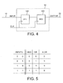
- circuitry 14 which comprises at least two flip-flops connected in series. That is, circuitry 14 comprises a first flip-flop 100 connected to receive the input 10 (which is the output from the first circuit 8) and the output of the first flip-flop is passed to the input of a second flip-flop 102. The output of the second flip-flop 102 is the output 20 of the return signal.
- the flip-flops are connected in series and are clocked by a common clock, which in the clock domain 12 will be clkB 18. The purpose of such a structural configuration of the circuitry 14 is to improve the so-called metastability within each of the clock domains.
- metastability can be understood by considering a register in which the input value changes asynchronously with respect to the clock. If the input value changes significantly before the clock edge, then the register will store the new value. However, if the input value changes significantly after the clock edge, then the register will use the old input value. Broadly speaking, metastability is concerned with the situation when the register input changes just as the clock edge arrives, in which case it is difficult to decide whether the register should store the new value or the old value.
- the problems associated with metastability are reduced using statistical probability. That is, in Figure 4 the probability that the input value will change close enough to the clock edge to cause a metastability condition is a finite value which can be determined based on the period of the particular clock signal in the physical parameters of the circuitry involved. However, by inserting a second flip-flop 102, the probability that a metastable condition in the first flip-flop 100 is still undecided by the time the clock edge arrives at the second flip-flop 102 is also known, since it is a function of the flip-flop itself and of the period.
- the probability that a metastable condition results is reduced. For example, for a circuit having two flip-flops connected in series as shown in Figure 4 it could be calculated that the probability value of a metastable condition occurring is 10 -9 . If a third flip-flop is added, the value becomes 10 -18 and thus the chance of a metastability condition arising is even further reduced.
- an embodiment of the present invention provides particularly advantageous applications in the field of set top boxes for television and video signals, wherein the clock frequencies are less than 100 MHz. It is therefore deemed appropriate for a metastability circuit having two flip-flops connected in series to be sufficient for clock signals having frequencies less than 100 MHz.
- Figure 1 shows that circuit 22 receives the return signals 20, 20' and 20" from the respective clock domains, and wherein the circuit 22 also comprises a metastability circuit having two flip-flops as shown in Figure 4, but which is now clocked by the first clock signal clkA 16. These return signals are thus clocked through circuit 22 by the first clock signal 16 and form part of a return synchronisation bus 30.
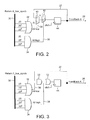
- the return synchronisation bus 30 is used by comparison circuitry 24, the structure of which is shown in Figure 2 according to a first embodiment. That is, an OR gate 32 and an AND gate circuitry 34 are connected to the return bus 30. Both the OR gate 32 and the AND gate 34 are capable of receiving the signals returned from each of the clock domains. That is OR gate 32 is capable of receiving the returned outputs 20, 20' and 20" from the respective circuitry in each of the corresponding clock domains. Likewise, AND gate 34 is capable of receiving each of the output signals 20, 20' and 20".
- the output 36 of the OR gate 32 is used to control a second multiplexer 40, whereas the output 38 from the AND gate 34 is used to control a third multiplexer 42.
- the third multiplexer having one input connected to a high signal, for example a high voltage, and having a second input connected to receive the output from the second multiplexer 40.
- the output of the third multiplexer 42 is an input of a latch circuit 44, which is clocked by the first clock signal clkA 16.
- the output of the latch 44 is known as the feedbackA signal 26, which on one hand is coupled to the input of a XOR gate 28, and on the other hand is fed back to a first input 27 of the second multiplexer 40.
- the second input of the second multiplexer 40 is connected to a low signal, for example a low voltage.
- the state "0" is transmitted to the other clock domains 12, 12' and 12", each being clocked with asynchronous clocking signals, which results in their corresponding return signals 20 changing to state "0" at different times.
- These return signals are then passed to synchronisation circuitry 22 which is clocked by the first clock signal onto a return synchronisation bus 30 shown in Figure 2.
- the OR gate 32 and the AND gate 34 continually monitors the state of the corresponding return signals on the bus 30, and when all of the return signals 20, 20' and 20" all have the state "0", then a "0” is produced at output 36 and also a "0” is produced at the output 38 of the AND gate 34.
- the second multiplexer 40 Since the output signal 36 is at "0", the second multiplexer 40 will select the second input (which is pulled low) and therefore a "0" will appear at the second input of the third multiplexer 42. Since the output signal 38 from the AND gate 34 is also at “0" the third multiplexer 42 will select the second input of the third multiplexer 42 and thus a "0" will propagate through the third multiplexer 42 to the input of the latch circuitry 44 and will be clocked out by the first clock 16.
- the state of the signal 26 from the comparison circuitry 24 is received at a first input of the XOR gate 28 and at this point in time will be at a "0" (as expected).
- the XOR gate 28 is connected to receive a second input from the output 10 of the first circuit 8.
- the XOR gate then compares the states of the first and second input and provides an update signal to the control the multiplexer circuitry 4.
- the update signal is set/reset depending, for example, on the logic functionality shown in Figure 5.
- both of the inputs to XOR gate 28 are "0" and therefore the output of the XOR gate will also produce a "0" which will control the multiplexer 4 so that the next bit in the bit stream is allowed to pass through the multiplexer 4 onto the input 6 of the first circuit 8.
- the circuit shown in Figure 2 allows the states of the signals returned from the various clock domains to be monitored until such time as they are all the same (i.e. synchronised), at which time the multiplexer circuitry 4 is controlled to allow the next signal in the signal sequence 2 to be transferred to the first circuit 8.
- the efficiency of the integrated circuit as a whole is optimised, since the next signal in the sequence is updated as soon as the outputs from the other clock domains are synchronised.
- the multiplexer 42 Since the output 38 of the AND gate 34 is "1", the multiplexer 42 will select its first output which is pulled high and therefore a "1" will arrive at the input of the latch circuit 44 which is clocked by the first clock signal 16 to the output 26.
- the output 26 of the comparison circuitry 24 will be a "1" which is one input of the XOR gate 28 and the second input to the XOR gate derives from the output 10 of the first circuit 8 (which will also be at a state of "1 "). If both of the inputs of the XOR gate 28 have a state of "1” then the output from the XOR gate 28 will be a "0" which indicates that the next bit in the bit stream 2 can be passed through the multiplexer 4 to the input 6 of the first circuit 8.
- next bit in the bit stream 2 i.e. the third bit
- the output signal 20" returned from the clock domain 12" has settled at the same state as that of the signal at the output 10 of the first circuit 8.
- Figure 3 shows an alternative embodiment of the comparison circuitry 24, wherein the second and third multiplexers 40, 42 are now replaced with an AND gate 50 and an OR gate 52 respectively. If one considers the same sequence of bits as described in relation to Figure 2, then the first bit is at state “0" and is propagated through the first circuit 8 to the output 10, and simultaneously transferred to all of the other clock domains 12, 12' and 12".
- the comparison circuitry 24 monitors the synchronisation bus 30 until such time as all of the inputs are low (i.e. "0"), wherein the output from the OR gate 32 and the AND gate 34 will be at "0".
- the output from the OR gate 32 forms a first input to the AND gate 50, whereas the output 38 of the AND gate 34 forms a first input to the OR gate 52.
- a second input of the OR gate 52 is formed from the output of the AND gate 50.
- the output of the OR gate 52 forms an input to the latch circuitry 44 which is clocked by the first clock signal 16, and the output of the latch circuitry 44 forms, on one hand an output signal 26 to produce a first input to XOR gate 28, and on the other hand is fed back to form a second input 27 of the AND gate 50.
- the next bit is a "1" which is propagated to an output 10 of the first circuit 8 and is then simultaneously transferred to all of the clock domains 12, 12', 12".
- the comparison circuitry 24 then monitors the synchronisation bus 30 until the signals returned from all of the respective clock domains have a state of "1". At this time both of the outputs 36 and 38 have a state of "1". Since the first input of the AND gate will be fed back from the output of the latch circuit 44 (which will be the state of the first bit in the bit stream, i.e. "0"), then the output of the AND gate 50 will be "0".
- sequence of signals 2 need not necessarily be a bit stream and could in fact be a plurality of messages in which case the circuitry the comparison circuitry determines when the messages received from the plurality of other domains meet a predetermined state at the output of the first circuit.
- the signal sequence 2 is often a control signal.
- control signals are returned and allowed to settle (in the various domains) before any further control signals in the sequence are sent.
- circuitry of the present application is particularly advantageous over software implementations, since the control of the signal to be transferred to a plurality of domains is inherent in the circuitry and therefore does not need to be taken into account using any software algorithms.
- Embodiments of the present invention can find application in different types of electronic circuits, for example counters, clock recovery circuits, etc.
- Example of multi-clock environments include digital media circuits, which for example may have different video, audio, picture domains.
- Embodiments of the present application find particularly useful application in integrated circuits (IC's), set top boxes (STB's) and digital video disk (DVD) units.
- IC's integrated circuits
- STB's set top boxes
- DVD digital video disk
Landscapes
- Engineering & Computer Science (AREA)
- Computer Networks & Wireless Communication (AREA)
- Signal Processing (AREA)
- Information Transfer Systems (AREA)
Priority Applications (4)
| Application Number | Priority Date | Filing Date | Title |
|---|---|---|---|
| DE602004007494T DE602004007494D1 (de) | 2004-05-24 | 2004-05-24 | Asynchrones Mehrfachtaktsystem |
| EP04253042A EP1601131B1 (de) | 2004-05-24 | 2004-05-24 | Asynchrones Mehrfachtaktsystem |
| US11/137,105 US7545896B2 (en) | 2004-05-24 | 2005-05-24 | Asynchronous multi-clock system |
| US12/481,375 US7929655B2 (en) | 2004-05-24 | 2009-06-09 | Asynchronous multi-clock system |
Applications Claiming Priority (1)
| Application Number | Priority Date | Filing Date | Title |
|---|---|---|---|
| EP04253042A EP1601131B1 (de) | 2004-05-24 | 2004-05-24 | Asynchrones Mehrfachtaktsystem |
Publications (2)
| Publication Number | Publication Date |
|---|---|
| EP1601131A1 true EP1601131A1 (de) | 2005-11-30 |
| EP1601131B1 EP1601131B1 (de) | 2007-07-11 |
Family
ID=34930335
Family Applications (1)
| Application Number | Title | Priority Date | Filing Date |
|---|---|---|---|
| EP04253042A Expired - Lifetime EP1601131B1 (de) | 2004-05-24 | 2004-05-24 | Asynchrones Mehrfachtaktsystem |
Country Status (3)
| Country | Link |
|---|---|
| US (2) | US7545896B2 (de) |
| EP (1) | EP1601131B1 (de) |
| DE (1) | DE602004007494D1 (de) |
Families Citing this family (6)
| Publication number | Priority date | Publication date | Assignee | Title |
|---|---|---|---|---|
| DE602004007494D1 (de) * | 2004-05-24 | 2007-08-23 | Sgs Thomson Microelectronics | Asynchrones Mehrfachtaktsystem |
| US7639764B2 (en) * | 2005-08-17 | 2009-12-29 | Atmel Corporation | Method and apparatus for synchronizing data between different clock domains in a memory controller |
| US7812682B2 (en) * | 2009-03-05 | 2010-10-12 | Nel Frequency Controls, Inc. | Crystal-based oscillator for use in synchronized system |
| US8072273B2 (en) * | 2009-03-05 | 2011-12-06 | Nel Frequency Controls, Inc. | System employing synchronized crystal oscillator-based clock, to be used in either discrete or integrated applications |
| US8255702B1 (en) | 2009-12-03 | 2012-08-28 | Altera Corporation | Programmable logic device with improved security |
| US9607674B1 (en) * | 2016-01-06 | 2017-03-28 | Qualcomm Incorporated | Pulse latch reset tracking at high differential voltage |
Citations (2)
| Publication number | Priority date | Publication date | Assignee | Title |
|---|---|---|---|---|
| EP1071005A2 (de) * | 1999-07-19 | 2001-01-24 | Thomson Licensing S.A. | Datenübertragungsvorrichtung für ein System mit mehreren Taktbereichen |
| WO2001079987A1 (en) * | 2000-04-17 | 2001-10-25 | Italtel S.P.A. | Two clock domain pulse to pulse synchronizer |
Family Cites Families (8)
| Publication number | Priority date | Publication date | Assignee | Title |
|---|---|---|---|---|
| US5256912A (en) * | 1991-12-19 | 1993-10-26 | Sun Microsystems, Inc. | Synchronizer apparatus for system having at least two clock domains |
| US5448715A (en) * | 1992-07-29 | 1995-09-05 | Hewlett-Packard Company | Dual clock domain interface between CPU and memory bus |
| SG47976A1 (en) * | 1994-05-10 | 1998-04-17 | Intel Corp | Method and apparatus for providing synchronous data transmission between digital devices operating at frequencies having a p/q integer ratio relationship |
| US6260152B1 (en) * | 1998-07-30 | 2001-07-10 | Siemens Information And Communication Networks, Inc. | Method and apparatus for synchronizing data transfers in a logic circuit having plural clock domains |
| US6370600B1 (en) * | 1999-05-25 | 2002-04-09 | Advanced Micro Devices, Inc. | Staging buffer for translating clock domains when source clock frequency exceeds target clock frequency |
| EP1124179B1 (de) * | 2000-02-09 | 2007-10-17 | Texas Instruments Incorporated | Gerät zur Signalsynchronisierung zwischen zwei Taktbereichen |
| US7027542B1 (en) * | 2001-06-04 | 2006-04-11 | Advanced Micro Devices, Inc. | Apparatus and method for providing data transfer between two digital circuits with different clock domains and for solving metastability problems |
| DE602004007494D1 (de) * | 2004-05-24 | 2007-08-23 | Sgs Thomson Microelectronics | Asynchrones Mehrfachtaktsystem |
-
2004
- 2004-05-24 DE DE602004007494T patent/DE602004007494D1/de not_active Expired - Lifetime
- 2004-05-24 EP EP04253042A patent/EP1601131B1/de not_active Expired - Lifetime
-
2005
- 2005-05-24 US US11/137,105 patent/US7545896B2/en active Active
-
2009
- 2009-06-09 US US12/481,375 patent/US7929655B2/en not_active Expired - Fee Related
Patent Citations (2)
| Publication number | Priority date | Publication date | Assignee | Title |
|---|---|---|---|---|
| EP1071005A2 (de) * | 1999-07-19 | 2001-01-24 | Thomson Licensing S.A. | Datenübertragungsvorrichtung für ein System mit mehreren Taktbereichen |
| WO2001079987A1 (en) * | 2000-04-17 | 2001-10-25 | Italtel S.P.A. | Two clock domain pulse to pulse synchronizer |
Non-Patent Citations (2)
| Title |
|---|
| SHENGXIAN ZHUANG ET AL: "An asynchronous wrapper with novel handshake circuits for GALS systems", 2002 INTERNATIONAL CONFERENCE ON COMMUNICATIONS, CIRCUITS AND SYSTEMS AND WEST SINO EXPOSITION, vol. 2, 29 June 2002 (2002-06-29), CHNGDU, CHINA, pages 1521 - 1525, XP010631809 * |
| SRIDHAR R: "System-on-chip (SoC): clocking and synchronization issues", 17TH INTERNATIONAL CONFERENCE ON VLSI DESIGN, 5 January 2004 (2004-01-05), MUMBAI, INDIA, pages 520 - 527, XP010679044 * |
Also Published As
| Publication number | Publication date |
|---|---|
| US20050280455A1 (en) | 2005-12-22 |
| DE602004007494D1 (de) | 2007-08-23 |
| US20090316845A1 (en) | 2009-12-24 |
| US7545896B2 (en) | 2009-06-09 |
| EP1601131B1 (de) | 2007-07-11 |
| US7929655B2 (en) | 2011-04-19 |
Similar Documents
| Publication | Publication Date | Title |
|---|---|---|
| US6696854B2 (en) | Methods and circuitry for implementing first-in first-out structure | |
| US7929655B2 (en) | Asynchronous multi-clock system | |
| US8350596B1 (en) | Clock loss detection circuit for PLL clock switchover | |
| CN106409325A (zh) | 用于源同步信息传送的装置和关联方法 | |
| US7007186B1 (en) | Systems and methods for synchronizing a signal across multiple clock domains in an integrated circuit | |
| US8514004B2 (en) | Clock management unit and method of managing a clock signal | |
| CN110311659A (zh) | 一种触发器及集成电路 | |
| US7783911B2 (en) | Programmable bus driver launch delay/cycle delay to reduce elastic interface elasticity requirements | |
| WO2013179089A1 (en) | Sequential logic circuit and method of providing setup timing violation tolerance therefor | |
| CN117435016A (zh) | 一种复位电路的设计方法 | |
| US7446588B2 (en) | Highly scalable methods and apparatus for multiplexing signals | |
| US7734944B2 (en) | Mechanism for windaging of a double rate driver | |
| US9626317B2 (en) | Arbiter for asynchronous state machines | |
| US6882184B2 (en) | Clock switching circuit | |
| JP2008300915A (ja) | クロックのデューティ比を活用した高速度シリアル通信 | |
| CN114637369B (zh) | 数据延迟补偿器电路 | |
| US6566924B2 (en) | Parallel push algorithm detecting constraints to minimize clock skew | |
| KR101006843B1 (ko) | 출력신호를 안정적으로 생성하는 동기화 회로 | |
| CN113359015B (zh) | 数字电路监测设备 | |
| CN111510116B (zh) | 电子装置和噪声去除系统 | |
| JP2011077791A (ja) | データ伝送システム及び方法、データ送信装置及び受信装置 | |
| JP2000082090A (ja) | 遅延機能付フリップフロップ回路、遅延機能付ラッチ回路、順序回路の設計方法、半導体集積回路におけるクロック信号配線の自動設計装置、及び、半導体集積回路におけるクロック信号配線の自動設計方法 | |
| KR100588375B1 (ko) | 셋업/홀드 타임 제어 회로 | |
| KR100609135B1 (ko) | 셋업/홀드 타임 제어 회로 | |
| JP2004029947A (ja) | クロック生成装置及びオーディオデータ処理装置 |
Legal Events
| Date | Code | Title | Description |
|---|---|---|---|
| PUAI | Public reference made under article 153(3) epc to a published international application that has entered the european phase |
Free format text: ORIGINAL CODE: 0009012 |
|
| AK | Designated contracting states |
Kind code of ref document: A1 Designated state(s): AT BE BG CH CY CZ DE DK EE ES FI FR GB GR HU IE IT LI LU MC NL PL PT RO SE SI SK TR |
|
| AX | Request for extension of the european patent |
Extension state: AL HR LT LV MK |
|
| 17P | Request for examination filed |
Effective date: 20060519 |
|
| AKX | Designation fees paid |
Designated state(s): DE FR GB IT |
|
| GRAP | Despatch of communication of intention to grant a patent |
Free format text: ORIGINAL CODE: EPIDOSNIGR1 |
|
| GRAS | Grant fee paid |
Free format text: ORIGINAL CODE: EPIDOSNIGR3 |
|
| GRAA | (expected) grant |
Free format text: ORIGINAL CODE: 0009210 |
|
| AK | Designated contracting states |
Kind code of ref document: B1 Designated state(s): DE FR GB IT |
|
| REG | Reference to a national code |
Ref country code: GB Ref legal event code: FG4D |
|
| REF | Corresponds to: |
Ref document number: 602004007494 Country of ref document: DE Date of ref document: 20070823 Kind code of ref document: P |
|
| ET | Fr: translation filed | ||
| PLBE | No opposition filed within time limit |
Free format text: ORIGINAL CODE: 0009261 |
|
| STAA | Information on the status of an ep patent application or granted ep patent |
Free format text: STATUS: NO OPPOSITION FILED WITHIN TIME LIMIT |
|
| 26N | No opposition filed |
Effective date: 20080414 |
|
| PG25 | Lapsed in a contracting state [announced via postgrant information from national office to epo] |
Ref country code: DE Free format text: LAPSE BECAUSE OF FAILURE TO SUBMIT A TRANSLATION OF THE DESCRIPTION OR TO PAY THE FEE WITHIN THE PRESCRIBED TIME-LIMIT Effective date: 20071012 |
|
| PG25 | Lapsed in a contracting state [announced via postgrant information from national office to epo] |
Ref country code: IT Free format text: LAPSE BECAUSE OF NON-PAYMENT OF DUE FEES Effective date: 20080531 |
|
| PGFP | Annual fee paid to national office [announced via postgrant information from national office to epo] |
Ref country code: GB Payment date: 20130424 Year of fee payment: 10 |
|
| PGFP | Annual fee paid to national office [announced via postgrant information from national office to epo] |
Ref country code: FR Payment date: 20130626 Year of fee payment: 10 |
|
| REG | Reference to a national code |
Ref country code: GB Ref legal event code: S117 Free format text: REQUEST FILED; REQUEST FOR CORRECTION UNDER SECTION 117 FILED ON 13 SEPTEMBER 2013 |
|
| REG | Reference to a national code |
Ref country code: GB Ref legal event code: S117 Free format text: CORRECTIONS ALLOWED; REQUEST FOR CORRECTION UNDER SECTION 117 FILED ON 13 SEPTEMBER 2013 ALLOWED ON 15 JANUARY 2014 |
|
| REG | Reference to a national code |
Ref country code: FR Ref legal event code: RM Effective date: 20140401 Ref country code: FR Ref legal event code: CA Effective date: 20140401 |
|
| GBPC | Gb: european patent ceased through non-payment of renewal fee |
Effective date: 20140524 |
|
| REG | Reference to a national code |
Ref country code: FR Ref legal event code: ST Effective date: 20150130 |
|
| PG25 | Lapsed in a contracting state [announced via postgrant information from national office to epo] |
Ref country code: GB Free format text: LAPSE BECAUSE OF NON-PAYMENT OF DUE FEES Effective date: 20140524 Ref country code: FR Free format text: LAPSE BECAUSE OF NON-PAYMENT OF DUE FEES Effective date: 20140602 |