EP1603108A1 - Technique de commande pour affichage mixte couleur et monochrome - Google Patents
Technique de commande pour affichage mixte couleur et monochrome Download PDFInfo
- Publication number
- EP1603108A1 EP1603108A1 EP04102468A EP04102468A EP1603108A1 EP 1603108 A1 EP1603108 A1 EP 1603108A1 EP 04102468 A EP04102468 A EP 04102468A EP 04102468 A EP04102468 A EP 04102468A EP 1603108 A1 EP1603108 A1 EP 1603108A1
- Authority
- EP
- European Patent Office
- Prior art keywords
- region
- wireless communications
- communications device
- colour
- pixels
- Prior art date
- Legal status (The legal status is an assumption and is not a legal conclusion. Google has not performed a legal analysis and makes no representation as to the accuracy of the status listed.)
- Granted
Links
- 238000000034 method Methods 0.000 title claims description 26
- 238000004891 communication Methods 0.000 claims description 63
- 239000004973 liquid crystal related substance Substances 0.000 claims description 16
- 239000003086 colorant Substances 0.000 claims description 9
- 239000011159 matrix material Substances 0.000 claims description 6
- 238000005286 illumination Methods 0.000 claims description 3
- 230000006870 function Effects 0.000 description 12
- 238000003860 storage Methods 0.000 description 10
- 238000010586 diagram Methods 0.000 description 7
- 230000000007 visual effect Effects 0.000 description 5
- ORWQBKPSGDRPPA-UHFFFAOYSA-N 3-[2-[ethyl(methyl)amino]ethyl]-1h-indol-4-ol Chemical compound C1=CC(O)=C2C(CCN(C)CC)=CNC2=C1 ORWQBKPSGDRPPA-UHFFFAOYSA-N 0.000 description 4
- 230000008901 benefit Effects 0.000 description 4
- 238000012545 processing Methods 0.000 description 4
- 230000005540 biological transmission Effects 0.000 description 3
- 230000001965 increasing effect Effects 0.000 description 3
- 230000008569 process Effects 0.000 description 3
- 241001673391 Entandrophragma candollei Species 0.000 description 2
- 230000000694 effects Effects 0.000 description 2
- 230000002708 enhancing effect Effects 0.000 description 2
- 239000000463 material Substances 0.000 description 2
- 239000000758 substrate Substances 0.000 description 2
- 239000010409 thin film Substances 0.000 description 2
- 238000012546 transfer Methods 0.000 description 2
- 230000004075 alteration Effects 0.000 description 1
- 230000001413 cellular effect Effects 0.000 description 1
- 238000012505 colouration Methods 0.000 description 1
- 238000010276 construction Methods 0.000 description 1
- 230000003247 decreasing effect Effects 0.000 description 1
- 230000001419 dependent effect Effects 0.000 description 1
- 238000013461 design Methods 0.000 description 1
- 238000009826 distribution Methods 0.000 description 1
- 230000008030 elimination Effects 0.000 description 1
- 238000003379 elimination reaction Methods 0.000 description 1
- 238000005516 engineering process Methods 0.000 description 1
- 239000010408 film Substances 0.000 description 1
- 238000007429 general method Methods 0.000 description 1
- 238000009434 installation Methods 0.000 description 1
- 238000004519 manufacturing process Methods 0.000 description 1
- 238000002156 mixing Methods 0.000 description 1
- 238000012986 modification Methods 0.000 description 1
- 230000004048 modification Effects 0.000 description 1
- 238000001208 nuclear magnetic resonance pulse sequence Methods 0.000 description 1
- 230000003287 optical effect Effects 0.000 description 1
- 230000002085 persistent effect Effects 0.000 description 1
- 230000009467 reduction Effects 0.000 description 1
- 230000000630 rising effect Effects 0.000 description 1
- 230000005236 sound signal Effects 0.000 description 1
- 230000003068 static effect Effects 0.000 description 1
- 230000001360 synchronised effect Effects 0.000 description 1
Images




Classifications
-
- G—PHYSICS
- G09—EDUCATION; CRYPTOGRAPHY; DISPLAY; ADVERTISING; SEALS
- G09G—ARRANGEMENTS OR CIRCUITS FOR CONTROL OF INDICATING DEVICES USING STATIC MEANS TO PRESENT VARIABLE INFORMATION
- G09G3/00—Control arrangements or circuits, of interest only in connection with visual indicators other than cathode-ray tubes
- G09G3/20—Control arrangements or circuits, of interest only in connection with visual indicators other than cathode-ray tubes for presentation of an assembly of a number of characters, e.g. a page, by composing the assembly by combination of individual elements arranged in a matrix no fixed position being assigned to or needed to be assigned to the individual characters or partial characters
- G09G3/34—Control arrangements or circuits, of interest only in connection with visual indicators other than cathode-ray tubes for presentation of an assembly of a number of characters, e.g. a page, by composing the assembly by combination of individual elements arranged in a matrix no fixed position being assigned to or needed to be assigned to the individual characters or partial characters by control of light from an independent source
- G09G3/3406—Control of illumination source
- G09G3/3413—Details of control of colour illumination sources
-
- G—PHYSICS
- G09—EDUCATION; CRYPTOGRAPHY; DISPLAY; ADVERTISING; SEALS
- G09G—ARRANGEMENTS OR CIRCUITS FOR CONTROL OF INDICATING DEVICES USING STATIC MEANS TO PRESENT VARIABLE INFORMATION
- G09G3/00—Control arrangements or circuits, of interest only in connection with visual indicators other than cathode-ray tubes
- G09G3/20—Control arrangements or circuits, of interest only in connection with visual indicators other than cathode-ray tubes for presentation of an assembly of a number of characters, e.g. a page, by composing the assembly by combination of individual elements arranged in a matrix no fixed position being assigned to or needed to be assigned to the individual characters or partial characters
- G09G3/34—Control arrangements or circuits, of interest only in connection with visual indicators other than cathode-ray tubes for presentation of an assembly of a number of characters, e.g. a page, by composing the assembly by combination of individual elements arranged in a matrix no fixed position being assigned to or needed to be assigned to the individual characters or partial characters by control of light from an independent source
- G09G3/36—Control arrangements or circuits, of interest only in connection with visual indicators other than cathode-ray tubes for presentation of an assembly of a number of characters, e.g. a page, by composing the assembly by combination of individual elements arranged in a matrix no fixed position being assigned to or needed to be assigned to the individual characters or partial characters by control of light from an independent source using liquid crystals
- G09G3/3611—Control of matrices with row and column drivers
-
- G—PHYSICS
- G09—EDUCATION; CRYPTOGRAPHY; DISPLAY; ADVERTISING; SEALS
- G09G—ARRANGEMENTS OR CIRCUITS FOR CONTROL OF INDICATING DEVICES USING STATIC MEANS TO PRESENT VARIABLE INFORMATION
- G09G2310/00—Command of the display device
- G09G2310/02—Addressing, scanning or driving the display screen or processing steps related thereto
- G09G2310/0202—Addressing of scan or signal lines
- G09G2310/0213—Addressing of scan or signal lines controlling the sequence of the scanning lines with respect to the patterns to be displayed, e.g. to save power
-
- G—PHYSICS
- G09—EDUCATION; CRYPTOGRAPHY; DISPLAY; ADVERTISING; SEALS
- G09G—ARRANGEMENTS OR CIRCUITS FOR CONTROL OF INDICATING DEVICES USING STATIC MEANS TO PRESENT VARIABLE INFORMATION
- G09G2320/00—Control of display operating conditions
- G09G2320/06—Adjustment of display parameters
- G09G2320/0613—The adjustment depending on the type of the information to be displayed
-
- G—PHYSICS
- G09—EDUCATION; CRYPTOGRAPHY; DISPLAY; ADVERTISING; SEALS
- G09G—ARRANGEMENTS OR CIRCUITS FOR CONTROL OF INDICATING DEVICES USING STATIC MEANS TO PRESENT VARIABLE INFORMATION
- G09G2330/00—Aspects of power supply; Aspects of display protection and defect management
- G09G2330/02—Details of power systems and of start or stop of display operation
- G09G2330/021—Power management, e.g. power saving
-
- G—PHYSICS
- G09—EDUCATION; CRYPTOGRAPHY; DISPLAY; ADVERTISING; SEALS
- G09G—ARRANGEMENTS OR CIRCUITS FOR CONTROL OF INDICATING DEVICES USING STATIC MEANS TO PRESENT VARIABLE INFORMATION
- G09G3/00—Control arrangements or circuits, of interest only in connection with visual indicators other than cathode-ray tubes
- G09G3/20—Control arrangements or circuits, of interest only in connection with visual indicators other than cathode-ray tubes for presentation of an assembly of a number of characters, e.g. a page, by composing the assembly by combination of individual elements arranged in a matrix no fixed position being assigned to or needed to be assigned to the individual characters or partial characters
- G09G3/34—Control arrangements or circuits, of interest only in connection with visual indicators other than cathode-ray tubes for presentation of an assembly of a number of characters, e.g. a page, by composing the assembly by combination of individual elements arranged in a matrix no fixed position being assigned to or needed to be assigned to the individual characters or partial characters by control of light from an independent source
- G09G3/36—Control arrangements or circuits, of interest only in connection with visual indicators other than cathode-ray tubes for presentation of an assembly of a number of characters, e.g. a page, by composing the assembly by combination of individual elements arranged in a matrix no fixed position being assigned to or needed to be assigned to the individual characters or partial characters by control of light from an independent source using liquid crystals
- G09G3/3611—Control of matrices with row and column drivers
- G09G3/3674—Details of drivers for scan electrodes
- G09G3/3677—Details of drivers for scan electrodes suitable for active matrices only
Definitions
- the present invention relates to the field of liquid crystal display and, particularly, to the field of multi-mode operation of a liquid crystal display screen.
- High resolution displays with high refresh rates are susceptible to substantial power losses due to switching inefficiencies associated with driving many pixels on a display at high frequency. For example, 80-90% of power requirements of a field-sequential display, excluding backlight illumination, are related to switching losses associated when the screen is refreshed at a rate such as 2500 Hz. Field-sequential display switching power losses are 5 to 10 times greater than the power losses in conventional liquid crystal displays based on colour filters.
- This invention addresses the problem of reducing the switching losses and, therefore, power requirements of a display while maintaining or increasing visual quality.
- Switching losses associated with refreshing the screen at high rates can be reduced if the active area of the display can be categorized into regions such that each region can be electrically driven differently.
- this invention reduces switching losses by driving pixels in each region by an algorithm that minimizes power consumption while maintaining optical performance appropriate to the region's category. In this way, dynamic, high-power, high-refresh requirements can be isolated to regions containing colour or video, while low power, low refresh rates are applied to regions containing static "black and white" or monochrome text.
- the active area may be categorized into different regions, such as colour and monochrome regions. Therefore, images containing both types of regions can be driven in "Partial Colour Mode.”
- the regions may be of different bit colour depths and different refresh rates.
- the field-sequential display is updated at 2500 Hz and regions driven at this rate are capable of full colour video at 83 Hz.
- This dynamic, full colour capability is not required to display monochrome text.
- the refresh rate can be safely reduced to 250 Hz (possibly 55 Hz) without loss in visual quality.
- visual quality may be improved if the driving waveforms are optimized to improve contrast in monochrome regions to benefit the display of data such as text.
- Partial Colour Mode can be implemented by a gate driver and controller to allow certain gate lines to be activated less frequently to reduce the refresh rate on the associated portions of the display.
- the present invention relates to a method and device, especially a mobile station such as a handheld communications device, that practices the method for reducing power switching losses in a display.
- the display is a liquid crystal display and the light source includes light emitting diodes (LEDs) of different colours.
- the liquid crystal display may be operated at a rate of 30 or more frames per second.
- the LCD controller provides a train of pulses during each frame that may be varied in number or length or both. The number of pulses or pulse width of a single pulse may be used to vary the grey scale of a pixel.
- the LEDs of the light source preferably will include red, green, and blue colours. Other colour schemes, such as cyan, magenta, and yellow, are contemplated by the present invention.
- the present invention may be implemented by adapting the LCD controller to drive the gate lines differently in a frame. Although the present invention is directed to a liquid crystal display per se, the preferred use of the LCD is in a mobile station.
- FIG. 1 is a block diagram of a communication system 100 that includes a mobile station 102 that communicates through a wireless communication network.
- Mobile station 102 preferably includes a visual display 112, a keyboard 114, and perhaps one or more auxiliary user interfaces (UI) 116, each of which is coupled to a controller 106.
- Controller 106 is also coupled to radio frequency (RF) transceiver circuitry 108 and an antenna 110.
- RF radio frequency
- controller 106 is embodied as a central processing unit (CPU) which runs operating system software in a memory component (not shown). Controller 106 will normally control overall operation of mobile station 102, whereas signal processing operations associated with communication functions are typically performed in RF transceiver circuitry 108. Controller 106 interfaces with device display 112 to display received information, stored information, user inputs, and the like. Keyboard 114, which may be a telephone type keypad or full alphanumeric keyboard, is normally provided for entering data for storage in mobile station 102, information for transmission to network, a telephone number to place a telephone call, commands to be executed on mobile station 102, and possibly other or different user inputs.
- CPU central processing unit
- memory component not shown
- Controller 106 will normally control overall operation of mobile station 102, whereas signal processing operations associated with communication functions are typically performed in RF transceiver circuitry 108. Controller 106 interfaces with device display 112 to display received information, stored information, user inputs, and the like.
- Keyboard 114 which may be
- Mobile station 102 sends communication signals to and receives communication signals from the wireless network over a wireless link via antenna 110.
- RF transceiver circuitry 108 performs functions similar to those of a base station and a base station controller (BSC) (not shown), including for example modulation/demodulation and possibly encoding/decoding and encryption/decryption. It is also contemplated that RF transceiver circuitry 108 may perform certain functions in addition to those performed by a BSC. It will be apparent to those skilled in art that RF transceiver circuitry 108 will be adapted to particular wireless network or networks in which mobile station 102 is intended to operate.
- BSC base station controller
- Mobile station 102 includes a battery interface (IF) 134 for receiving one or more rechargeable batteries 132.
- Battery 132 provides electrical power to electrical circuitry in mobile station 102, and battery IF 132 provides for a mechanical and electrical connection for battery 132.
- Battery IF 132 is coupled to a regulator 136 which regulates power to the device.
- an RF transmitter of RF transceiver circuitry 108 is typically keyed or turned on only when it is sending to network, and is otherwise turned off to conserve resources.
- an RF receiver of RF transceiver circuitry 108 is typically periodically turned off to conserve power until it is needed to receive signals or information (if at all) during designated time periods.
- SIM 140 Subscriber Identity Module
- IF SIM interface
- SIM 140 is one type of a conventional "smart card" used to identify an end user (or subscriber) of mobile station 102 and to personalize the device, among other things. Without SIM 140, the mobile station terminal is not fully operational for communication through the wireless network. By inserting SIM 140 into mobile station 102, an end user can have access to any and all of his/her subscribed services.
- SIM 140 generally includes a processor and memory for storing information. Since SIM 140 is coupled to SIM IF 142, it is coupled to controller 106 through communication lines 144.
- SIM 140 contains some user parameters such as an International Mobile Subscriber Identity (IMSI).
- IMSI International Mobile Subscriber Identity
- An advantage of using SIM 140 is that end users are not necessarily bound by any single physical mobile station.
- SIM 140 may store additional user information for the mobile station as well, including datebook (or calendar) information and recent call information.
- Mobile station 102 may consist of a single unit, such as a data communication device, a multiple-function communication device with data and voice communication capabilities, a personal digital assistant (PDA) enabled for wireless communication, or a computer incorporating an internal modem.
- mobile station 102 may be a multiple-module unit comprising a plurality of separate components, including but in no way limited to a computer or other device connected to a wireless modem.
- RF transceiver circuitry 108 and antenna 110 may be implemented as a radio modem unit that may be inserted into a port on a laptop computer.
- the laptop computer would include display 112, keyboard 114, one or more auxiliary UIs 116, and controller 106 embodied as the computer's CPU. It is also contemplated that a computer or other equipment not normally capable of wireless communication may be adapted to connect to and effectively assume control of RF transceiver circuitry 108 and antenna 110 of a single-unit device such as one of those described above. Such a mobile station 102 may have a more particular implementation as described later in relation to mobile station 202 of FIG. 2.
- FIG. 2 is a detailed block diagram of a preferred mobile station 202.
- Mobile station 202 is preferably a two-way communication device having at least voice and advanced data communication capabilities, including the capability to communicate with other computer systems. Depending on the functionality provided by mobile station 202, it may be referred to as a data messaging device, a two-way pager, a cellular telephone with data messaging capabilities, a wireless Internet appliance, or a data communication device (with or without telephony capabilities). Mobile station 202 may communicate with any one of a plurality of fixed transceiver stations 200 within its geographic coverage area.
- Mobile station 202 will normally incorporate a communication subsystem 211, which includes a receiver, a transmitter, and associated components, such as one or more (preferably embedded or internal) antenna elements and, local oscillators (LOs), and a processing module such as a digital signal processor (DSP) (all not shown).
- Communication subsystem 211 is analogous to RF transceiver circuitry 108 and antenna 110 shown in FIG. 1. As will be apparent to those skilled in field of communications, particular design of communication subsystem 211 depends on the communication network in which mobile station 202 is intended to operate.
- SIM 262 includes those features described in relation to FIG. 1.
- Mobile station 202 is a battery-powered device so it also includes a battery IF 254 for receiving one or more rechargeable batteries 256.
- battery IF 254 provides electrical power to most if not all electrical circuitry in mobile station 202, and battery IF 254 provides for a mechanical and electrical connection for it.
- the battery IF 254 is coupled to a regulator (not shown) which provides power V+ to all of the circuitry.
- Mobile station 202 includes a microprocessor 238 (which is one implementation of controller 106 of FIG. 1) which controls overall operation of mobile station 202. Communication functions, including at least data and voice communications, are performed through communication subsystem 211. Microprocessor 238 also interacts with additional device subsystems such as a display 222, a flash memory 224, a random access memory (RAM) 226, auxiliary input/output (I/O) subsystems 228, a serial port 230, a keyboard 232, a speaker 234, a microphone 236, a short-range communications subsystem 240, and any other device subsystems generally designated at 242. Some of the subsystems shown in FIG. 2 perform communication-related functions, whereas other subsystems may provide "resident" or on-device functions.
- RAM random access memory
- I/O auxiliary input/output subsystems 228, a serial port 230, a keyboard 232, a speaker 234, a microphone 236, a short-range communications subsystem 240, and any other device subsystems
- keyboard 232 and display 222 may be used for both communication-related functions, such as entering a text message for transmission over a communication network, and device-resident functions such as a calculator or task list.
- Operating system software used by microprocessor 238 is preferably stored in a persistent store such as flash memory 224, which may alternatively be a read-only memory (ROM) or similar storage element (not shown).
- flash memory 224 may alternatively be a read-only memory (ROM) or similar storage element (not shown).
- ROM read-only memory
- RAM 226 volatile store
- a preferred application that may be loaded onto mobile station 202 may be a personal information manager (PIM) application having the ability to organize and manage data items relating to the user such as, but not limited to, instant messaging (IM), e-mail, calendar events, voice mails, appointments, and task items.
- PIM personal information manager
- IM instant messaging
- SIM 262 to facilitate storage of PIM data items and other information.
- the PIM application preferably has the ability to send and receive data items via the wireless network.
- PIM data items are seamlessly integrated, synchronized, and updated via the wireless network, with the mobile station user's corresponding data items stored and/or associated with a host computer system thereby creating a mirrored host computer on mobile station 202 with respect to such items. This is especially advantageous where the host computer system is the mobile station user's office computer system.
- Additional applications may also be loaded onto mobile station 202 through network 200, an auxiliary I/O subsystem 228, serial port 230, short-range communications subsystem 240, or any other suitable subsystem 242, and installed by a user in RAM 226 or preferably a non-volatile store (not shown) for execution by microprocessor 238.
- Such flexibility in application installation increases the functionality of mobile station 202 and may provide enhanced on-device functions, communication-related functions, or both.
- secure communication applications may enable electronic commerce functions and other such financial transactions to be performed using mobile station 202.
- a received signal such as a text message, an e-mail message, or web page download will be processed by communication subsystem 211 and input to microprocessor 238.
- Microprocessor 238 will preferably further process the signal for output to display 222, to auxiliary I/O device 228 or both as described further herein below with reference to Figures 3-7.
- a user of mobile station 202 may also compose data items, such as e-mail messages, for example, using keyboard 232 in conjunction with display 222 and possibly auxiliary I/O device 228.
- Keyboard 232 is preferably a complete alphanumeric keyboard and/or telephone-type keypad. These composed items may be transmitted over a communication network through communication subsystem 211.
- mobile station 202 For voice communications, the overall operation of mobile station 202 is substantially similar, except that the received signals would be output to speaker 234 and signals for transmission would be generated by microphone 236.
- Alternative voice or audio I/O subsystems such as a voice message recording subsystem, may also be implemented on mobile station 202.
- voice or audio signal output is preferably accomplished primarily through speaker 234, display 222 may also be used to provide an indication of the identity of a calling party, duration of a voice call, or other voice call related information, as some examples.
- Serial port 230 in FIG. 2 is normally implemented in a personal digital assistant (PDA)-type communication device for which synchronization with a user's desktop computer is a desirable, albeit optional, component.
- Serial port 230 enables a user to set preferences through an external device or software application and extends the capabilities of mobile station 202 by providing for information or software downloads to mobile station 202 other than through a wireless communication network.
- the alternate download path may, for example, be used to load an encryption key onto mobile station 202 through a direct and thus reliable and trusted connection to thereby provide secure device communication.
- Short-range communications subsystem 240 of FIG. 2 is an additional optional component which provides for communication between mobile station 202 and different systems or devices, which need not necessarily be similar devices.
- subsystem 240 may include an infrared device and associated circuits and components, or a BluetoothTM communication module to provide for communication with similarly-enabled systems and devices.
- BluetoothTM is a registered trademark of Bluetooth SIG, Inc.
- mobile station 202 is a multitasking handheld wireless communications device configured for sending and receiving data items and for making and receiving voice calls.
- an operating system resident on station 202 (not shown) provides a GUI having a main screen and a plurality of sub-screens navigable from the main screen.
- the liquid crystal display cell 222 is shown in greater detail in Figure 3 in which a light source formed from multiple LEDs 322, 324, 326 is used as a backlight.
- LCD controller 316 provides a voltage to the common electrode(s) 308 and the active elements 310 of the active matrix.
- the active elements are preferably thin film transistors.
- the common electrode(s) 308 and active elements are supported on substrates 306 and 312, respectively.
- the LCD preferably contains a brightness enhancing film or layer 304 to optimize the distribution of light for a viewer.
- polarizers 302 and 314 are used as the preferred liquid crystal material is super twisted nematic.
- the LCD controller 316 sets the pixel grey scale of the LCD.
- An optional processor 318 may coordinate synchronization of the LCD controller 316 with the light source controller 320.
- the LCD controller 316 and the processor 318 are integrated into a single device 317, which may simply be referred to as an LCD controller having the capability of controlling a light source controller 320.
- the light source may be implemented by using red, green, and blue LEDs 322, 324, 326. In a specific embodiment, four green, four red, and two blue LEDs are used to provide full colour and/or black and white display.
- the LED controller 320 may sequence the three colours or may simultaneously energized LEDs of all of the colours and terminate power to the LEDs simultaneously. Other combinations of LEDs are contemplated by the present invention.
- the light guide 328 may have a tapered block construction and may have approximately a trapezoidal form to more evenly distribute the light into the LCD.
- the light guide may also have uneven areas 330, 332 that scatter the light so as to avoid shadowing effects in the LCD image.
- uneven area 330 is shown to project out from the surface of the light guide 328 and uneven area 332 is shown to project inward to the surface of the light guide 328, the uneven areas may be arranged differently so long as the arrangement effectively scatters the light from the LEDs 322, 324, 326.
- the uneven areas may be abraded, molded, corrugated, chemically etched, or the like.
- the LEDs 322, 324, 326 and the light guide 328 are partially enclosed by a reflector such that the only opening is fully bounded by the light transmissive area of the LCD.
- FIG 4 illustrates an embodiment of the LCD controller 402 and LCD 430 for the method of the present invention.
- the LED controller may be internally adapted to provide a sequence of lights each centered on a specific wavelength according to the LEDs energized, followed by light generated simultaneously from all LEDs or at least two LEDs generating light centered on two different wavelengths.
- the LCD controller 402 in synchronization with the LED controller, creates a grey scale pattern for each light centred on a specific wavelength according to column driver 410 (source driver) and row selectors 412-422 (gate driver) in a X-Y matrix arrangement. For a red light pattern, only pixels selectable by the column driver 410 may be set to a transmissive state to provide a desired pattern.
- Pixels that do not have a red component of light are turned off. For green and blue light patterns, similar procedures are followed. When all red, green, and blue colours are transmitted through a given pixel, that pixel may have a white or whitish appearance because of the blending of the three primary colours perceived by a viewer.
- Advantages in using the light source to determine colours include elimination of a colour filter layer, thus enhancing brightness of the display by reducing a light absorbing layer, and increasing the resolution as only one pixel is needed to provide full colour instead of separate red, green, and blue pixels.
- the size of a pixel is allowed to increase while resolution is improved; in other words, using the light source and not the LCD to determine colour optimizes substrate real estate usage.
- the method of the present invention is generally shown in Figure 5. Although this embodiment is directed to the division of the LCD screen into monochrome and colour regions, other schemes are contemplated such as high bit rate colour, low bit rate colour, mono colour, etc.
- a processor designates certain lines as colour 502 or monochrome 504. Remaining lines are considered to be in an off state 506. If the display screen is operational in a display mode 508, then all colour lines are scanned 510 before any monochrome lines are scanned 512. The reason the colour lines are scanned first is because they have a clocking scheme that is different than the monochrome lines. In other embodiments, monochrome lines may be scanned before colour lines.
- the new configuration is determined by repeating steps 502-506. Scanning in a colour region involves a first sweep of each line in the region before any of the lines in the colour region are swept a second or successive time.
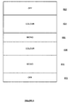
- FIG. 6 illustrates an embodiment of the general display screen in the present invention.
- the top and bottom regions of the display 602, 612 are turned off.
- the colouration of the off region is dependent upon the characteristics of the unbiased liquid crystal material and the orientation of any polarizers.
- a colour region 604, a monochrome region 606, another colour region 608, and another monochrome region 610 are located between the top and bottom off regions 602, 612.
- the display screen is basically divided into horizontal bands that are in one of three modes: colour, monochrome, or off.
- the display screen may be divided into a monochrome region and an off region, a monochrome region and a colour region, or a colour region and an off region.
- Figure 7 illustrates a block diagram an embodiment of the LCD controller elements and the LCD.
- the grey level for the pixels is provided through the source driver 704.
- a memory 712 is used to provide image data.
- the memory may be volatile, such as random access memory, or non-volatile, such as read only memory.
- the image data is used to access a bit pattern for providing grey scale or toggling for a pixel through a lookup table.
- Lookup table A 708 provides a pattern of multiple bits representing or correlating to a grey scale value.
- the bits in a pattern number at least six and may be eight, ten, twelve, or sixteen in number.
- Lookup table B 710 provides a single bit or bit sequence representing an on or off state for a pixel in a monochrome region or line on the display screen.
- an off state value may be provided in which the source driver will not bias the liquid crystal display pixel selected by switch (i.e., multiplexer) 706.
- the gate line driver operates to sweep each of the two types of scannable regions separately. That is, the colour region scan sequence storage element 724 will be accessed and used to scan the designated portions of the display screen 702 before or after the monochrome sequence storage element 726 is accessed for scanning. The monochrome scan sequence storage element 726 is scanned at a rate different than the rate for the colour sequence storage element 724.
- Switch 722 provides the correct sequence to the gate driver 720, and, optionally during the remaining time, disables the gate for OFF regions.
- FIG. 8 illustrates a colour only mode in which either the entire display screen is in colour or the non-colour portion of the display screen is in the off state.
- pixel grey scale is achieved through pulses written to a pixel during scanning.
- Each colour frame 802 is divided into three parts (or fields) 804, 806, 808 for the three colours in full colour mode.
- Each pixel to be illuminated by a specific colour of light achieves a grey scale value from a pulse pattern into the source of the thin film transistor providing charge to the pixel.
- the pulse pattern i.e., colour scans
- One pulse is applied to each colour pixel during a scan of the colour region that includes the colour pixel.
- the actual scanning occupies most of the time allotted 830 for a given colour. It is the successive scans of the colour pixels during a frame that establishes a grey scale value. A smaller portion of the time allotted in a scan period is idle time 834.
- the light source is turned off 814. In alternative embodiments, the light source may remain on for most or all of the scan period and/or the actual scanning may occupy a different portion of the time allotted for a given colour.
- the light source e.g., light emitting diode
- the common electrode of the display is inverted from a first voltage bias level 822 to a second voltage bias level 824 to prevent charge buildup in the liquid crystal that would degrade performance and damage the display.
- the inversion of the common electrode voltage occurs for each colour for each frame.
- the common electrode voltage is inverted three times.
- Other inversion modes are contemplated by the present invention such as line inversion and pixel inversion.
- a given line may be alternately supplied through the source driver with voltages from a first set of a polarity and then supplied with voltages from a second set of a polarity opposite to that of the first set; that is, a non-inverting pair of voltages may be applied and an inverting pair of voltages may later be applied.
- alternate columns may be supplied for each row with voltage sets of opposing polarities.
- FIGs 9 and 10 illustrate two embodiments for a single frame of the display having both monochrome and colour regions.
- the monochrome scan 916 occurs in which each pixel is activated once.
- one clock pulse is used to set an on or off value for the monochrome pixels, resulting in less switching power dissipation.
- the grey scale values are developed 914 by multiple pulses from the gate line driver in which the source driver is loaded with new data during the multiple scans corresponding to a single colour in a field.
- Figure 10 represents an alternative embodiment in which the monochrome and colour scans 1016, 1014 are the same as in Figure 9, but the light source is operated at lower power for a longer period of time 1004, 1008 with a short LED OFF time 1006.
- Figure 11 represents a more specific embodiment of the present invention in which the display screen is divided into relatively few regions in which pixels are activated by source driver 1102 and gate driver 1104. At the top and bottom of the display screen are off regions 1108, 1116. At the center of the display screen is a monochrome region 1112 between two colour regions 1110, 1114. Two output shift registers (e.g., serial in/ parallel out shift registers) A, B, as illustrated in Figure 12, are used for scanning the two colour regions. Shift register A 1210 and shift register B 1208 contain initialization values for the gate shift register of regions A and B, respectively. They preferably contain a one-hot encoding of the starting line number of their respective regions.
- shift register A 1210 and shift register B 1208 contain initialization values for the gate shift register of regions A and B, respectively. They preferably contain a one-hot encoding of the starting line number of their respective regions.
- one-hot encoding refers to a single active bit that is shifted through the shift register such that only one line at a time of pixels is written to from the source driver.
- First shift register A 1210 is loaded and then used to sweep the first colour region once, then shift register B 1208 is loaded and then used to sweep the second colour region once.
- the shift registers alternate until the number of scans in that frame have all been completed.
- the clock rate COLOUR LINE CLOCK is relatively high. For example, a 10 MHz clock may be used.
- the monochrome region is scanned using a slower clock MONO LINE CLOCK to enter a binary value into the pixel to cause the pixel to be on or off.
- a switch 1228 may be used to transfer either COLOUR LINE CLOCK or MONO LINE CLOCK to storage elements 1218, 1226 according to the region by the REGION SELECT signal in FIG. 7.
- the storage elements 1218, 1226 may be latches that latch data on the rising or falling edges of a clock, D type flip flops, or the like.
- Counters 1202-1206 are used to hold the number of lines in each region.
- each colour region is scanned multiple times before any other colour region is scanned.
- the monochrome region(s) is scanned before the colour region(s) is scanned.
- Figure 14 illustrates an overview of the embodiment of a method of the present invention corresponding to the display scanning system of Figure 12.
- initialization occurs 1404 (e.g., registers are initialized) and the three colour fields are cycled through 1406-1410 through successive scans during a frame.
- Mono regions may be updated during all, some, or a single one of the colour fields.
- Figure 13 illustrates a more detailed embodiment of the method of Figure 14.
- the gate clock is set equal to the COLOUR LINE CLOCK through switch 1228.
- the LOAD SOURCE PATTERN of FIG. 12 is deasserted 1302 to enable the OUTPUT SHIFT REGISTER to shift its data.
- the counters 1202-1206 are loaded, the number of scannings per colour are loaded, and the colour and monochrome storage elements 1208-1210 are loaded 1304.
- the light source is turned off 1306. Colour region B's count 1204 is loaded 1308.
- the gate clock is switched at the COLOUR LINE CLOCK rate 1312, the gate shift register is initialized 1314 to start scanning at the beginning of colour region B 1114 by using switch A and B (FIG. 12) and asserting LOAD SOURCE PATTERN (FIG. 12), and a succession of gate clocks causes each row of colour region B 1114 to receive a new source pattern 1507 which is used to load unique lines (rows) in colour region B 1114 of the display screen 1316.
- colour region A's counter is loaded and a similar process is repeated but for region A 1110 for each count of the counter, as long as the counter has not timed out 1320, 1322, 1324, 1326.
- the light source is turned on 1328, 1330.
- the common electrodes polarity is inverted 1346.
- a counter is loaded with the number of lines count M 1338 in the monochrome region and the monochrome region is scanned 1344 once, if the count is not zero, at a reduced clock rate 1342 that is determined by dividing the line clock by the number of scans per field to yield the MONO LINE CLOCK.
- the reduced clock rate may be established by other means and may occupy the idle time period.
- the serial in/ parallel out shift registers A, B may be loaded with counts, and then the mode is switched to partial colour.
- the gate driver output is disabled.
- the gate driver output is enabled.
- the gate clock is slowed.
- Each line of the monochrome region is driven until the end of the monochrome region is reached.
- the clock is switched to a fast gate clock relative to the monochrome region clock rate.
- Each line of the colour region B is driven until the end of colour region B.
- the output shift register is reset to SIPO A. Each line of colour region A is driven until the end of colour region A.
- the output shift register is reset to SIPO B unless the predetermined number of scans to achieve grey scale has been performed for the frame. If the predetermined number of scans has been reached, then the gate clock is disabled, the light source is turned on, and the common electrode is inverted. A determination is made as to whether to resume normal mode. If not, then partial colour mode is maintained and the processing begins again by slowing down the gate clock. Otherwise, normal mode is assumed in which the fast gate clock is used to control the pixel gates of the display and the gate driver output is disabled until the first line is ready for data transfer.
- M represents a monochrome region scan
- BA represents a scan of colour regions B and A
- the process may be depicted as: M BA BA BA BA BA BA BA BA BA BA BA BA BA BA BA BA BA BA BA BA BA BA BA invert wait - in which the light is turned on during the last one or last few of the colour region BA scans, the invert period, and the wait period.
- Figure 15 illustrates a more detailed embodiment of a scan for a field.
- the gate line driver is shifted once 1504.
- the load pattern is deasserted 1506.
- a new source pattern is loaded 1507.
- the source lines on the display matrix are driven 1508.
- the line count is reduced by one 1510. As long as the counter does not expire (e.g., the line count remains greater than zero in a count down mode) 1512, scanning resumes at step 1504.
Landscapes
- Engineering & Computer Science (AREA)
- Physics & Mathematics (AREA)
- Computer Hardware Design (AREA)
- General Physics & Mathematics (AREA)
- Theoretical Computer Science (AREA)
- Chemical & Material Sciences (AREA)
- Crystallography & Structural Chemistry (AREA)
- Control Of Indicators Other Than Cathode Ray Tubes (AREA)
Priority Applications (4)
| Application Number | Priority Date | Filing Date | Title |
|---|---|---|---|
| EP04102468.8A EP1603108B1 (fr) | 2004-06-02 | 2004-06-02 | Technique de commande pour affichage mixte couleur et monochrome |
| SG200503181A SG117594A1 (en) | 2004-06-02 | 2005-05-20 | Mixed monochrome and colour display driving technique |
| CA2508183A CA2508183C (fr) | 2004-06-02 | 2005-05-24 | Technique de commande d'affichage mixte monochrome et couleur |
| CN 200510075422 CN1705008B (zh) | 2004-06-02 | 2005-06-01 | 在显示器屏幕上实现多扫描模式的方法及无线通信设备 |
Applications Claiming Priority (1)
| Application Number | Priority Date | Filing Date | Title |
|---|---|---|---|
| EP04102468.8A EP1603108B1 (fr) | 2004-06-02 | 2004-06-02 | Technique de commande pour affichage mixte couleur et monochrome |
Publications (2)
| Publication Number | Publication Date |
|---|---|
| EP1603108A1 true EP1603108A1 (fr) | 2005-12-07 |
| EP1603108B1 EP1603108B1 (fr) | 2017-03-22 |
Family
ID=34929162
Family Applications (1)
| Application Number | Title | Priority Date | Filing Date |
|---|---|---|---|
| EP04102468.8A Expired - Lifetime EP1603108B1 (fr) | 2004-06-02 | 2004-06-02 | Technique de commande pour affichage mixte couleur et monochrome |
Country Status (4)
| Country | Link |
|---|---|
| EP (1) | EP1603108B1 (fr) |
| CN (1) | CN1705008B (fr) |
| CA (1) | CA2508183C (fr) |
| SG (1) | SG117594A1 (fr) |
Cited By (3)
| Publication number | Priority date | Publication date | Assignee | Title |
|---|---|---|---|---|
| US20120256940A1 (en) * | 2009-10-16 | 2012-10-11 | Samsung Lcd Netherlands R & D Center B.V. | Display device and display apparatus |
| TWI425488B (zh) * | 2009-11-03 | 2014-02-01 | Nuvoton Technology Corp | 場序顯示器的驅動器及其驅動方法 |
| CN113519181A (zh) * | 2019-02-28 | 2021-10-19 | 佳能株式会社 | 通信设备、通信方法及程序 |
Families Citing this family (9)
| Publication number | Priority date | Publication date | Assignee | Title |
|---|---|---|---|---|
| CN102346996B (zh) * | 2010-08-04 | 2013-12-25 | 深圳莱宝高科技股份有限公司 | 显示装置及其驱动电路 |
| KR101867494B1 (ko) * | 2012-10-05 | 2018-07-17 | 텍추얼 랩스 컴퍼니 | 저지연 유저 입력 프로세싱과 피드백용 하이브리드 시스템 및 방법 |
| US10482822B2 (en) | 2016-09-09 | 2019-11-19 | Apple Inc. | Displays with multiple scanning modes |
| US10109240B2 (en) | 2016-09-09 | 2018-10-23 | Apple Inc. | Displays with multiple scanning modes |
| CN106652972B (zh) | 2017-01-03 | 2020-06-05 | 京东方科技集团股份有限公司 | 显示屏的处理电路、显示方法及显示器件 |
| CN106782268B (zh) | 2017-01-04 | 2020-07-24 | 京东方科技集团股份有限公司 | 显示系统和用于显示面板的驱动方法 |
| CN107145192B (zh) | 2017-04-27 | 2021-01-15 | Oppo广东移动通信有限公司 | 电子装置 |
| CN112447145B (zh) * | 2019-08-29 | 2022-06-24 | 北京小米移动软件有限公司 | 显示面板,显示模式的切换方法及装置、电子设备 |
| CN114582252B (zh) * | 2022-02-28 | 2023-11-24 | 深圳市思坦科技有限公司 | 一种显示模块、显示面板及显示器 |
Citations (6)
| Publication number | Priority date | Publication date | Assignee | Title |
|---|---|---|---|---|
| EP0852371A1 (fr) * | 1995-09-20 | 1998-07-08 | Hitachi, Ltd. | Dispositif d'affichage d'images |
| US20010017604A1 (en) * | 1996-10-31 | 2001-08-30 | Jeffrey Jacobsen | Reflective microdisplay for portable communication system |
| EP1148468A1 (fr) * | 1999-09-27 | 2001-10-24 | Citizen Watch Co., Ltd. | Procede de commande d'un ecran a cristaux liquides couleur et procede de commande de l'affichage de la montre |
| WO2001091098A1 (fr) * | 2000-05-24 | 2001-11-29 | Hitachi, Ltd. | Terminal portable et afficheur commutable entre couleur et noir-et-blanc |
| US20030063077A1 (en) * | 2001-10-01 | 2003-04-03 | Jun Koyama | Display device and electric equipment using the same |
| US20040027346A1 (en) * | 2001-11-24 | 2004-02-12 | Rolf-Deiter Naske | Method and device for the generation of 3-D images |
Family Cites Families (5)
| Publication number | Priority date | Publication date | Assignee | Title |
|---|---|---|---|---|
| JPH07152340A (ja) * | 1993-11-30 | 1995-06-16 | Rohm Co Ltd | ディスプレイ装置 |
| US20010040538A1 (en) * | 1999-05-13 | 2001-11-15 | William A. Quanrud | Display system with multiplexed pixels |
| WO2001069584A1 (fr) * | 2000-03-14 | 2001-09-20 | Mitsubishi Denki Kabushiki Kaisha | Afficheur d'image et procede d'affichage d'image |
| EP1325093A2 (fr) * | 2000-09-26 | 2003-07-09 | Matsushita Electric Industrial Co., Ltd. | Ecran et son systeme de commande et ecran d'information |
| GB2378343B (en) * | 2001-08-03 | 2004-05-19 | Sendo Int Ltd | Image refresh in a display |
-
2004
- 2004-06-02 EP EP04102468.8A patent/EP1603108B1/fr not_active Expired - Lifetime
-
2005
- 2005-05-20 SG SG200503181A patent/SG117594A1/en unknown
- 2005-05-24 CA CA2508183A patent/CA2508183C/fr not_active Expired - Lifetime
- 2005-06-01 CN CN 200510075422 patent/CN1705008B/zh not_active Expired - Lifetime
Patent Citations (7)
| Publication number | Priority date | Publication date | Assignee | Title |
|---|---|---|---|---|
| EP0852371A1 (fr) * | 1995-09-20 | 1998-07-08 | Hitachi, Ltd. | Dispositif d'affichage d'images |
| US20010017604A1 (en) * | 1996-10-31 | 2001-08-30 | Jeffrey Jacobsen | Reflective microdisplay for portable communication system |
| EP1148468A1 (fr) * | 1999-09-27 | 2001-10-24 | Citizen Watch Co., Ltd. | Procede de commande d'un ecran a cristaux liquides couleur et procede de commande de l'affichage de la montre |
| WO2001091098A1 (fr) * | 2000-05-24 | 2001-11-29 | Hitachi, Ltd. | Terminal portable et afficheur commutable entre couleur et noir-et-blanc |
| US20040140972A1 (en) * | 2000-05-24 | 2004-07-22 | Shouichi Hirota | Color/black-and-white switchable portable terminal and display unit |
| US20030063077A1 (en) * | 2001-10-01 | 2003-04-03 | Jun Koyama | Display device and electric equipment using the same |
| US20040027346A1 (en) * | 2001-11-24 | 2004-02-12 | Rolf-Deiter Naske | Method and device for the generation of 3-D images |
Cited By (6)
| Publication number | Priority date | Publication date | Assignee | Title |
|---|---|---|---|---|
| US20120256940A1 (en) * | 2009-10-16 | 2012-10-11 | Samsung Lcd Netherlands R & D Center B.V. | Display device and display apparatus |
| US9153157B2 (en) * | 2009-10-16 | 2015-10-06 | Amazon Technologies, Inc. | Display device and display apparatus |
| TWI425488B (zh) * | 2009-11-03 | 2014-02-01 | Nuvoton Technology Corp | 場序顯示器的驅動器及其驅動方法 |
| US8643683B2 (en) | 2009-11-03 | 2014-02-04 | Nuvoton Technolgoy Corporation | Driver of field sequential display capable of switching current and voltage of scan signal and display signal and driving method thereof |
| CN113519181A (zh) * | 2019-02-28 | 2021-10-19 | 佳能株式会社 | 通信设备、通信方法及程序 |
| CN113519181B (zh) * | 2019-02-28 | 2023-07-25 | 佳能株式会社 | 通信设备、通信方法及计算机可读存储介质 |
Also Published As
| Publication number | Publication date |
|---|---|
| CA2508183C (fr) | 2010-11-23 |
| CN1705008B (zh) | 2010-04-28 |
| SG117594A1 (en) | 2005-12-29 |
| EP1603108B1 (fr) | 2017-03-22 |
| CN1705008A (zh) | 2005-12-07 |
| CA2508183A1 (fr) | 2005-12-02 |
Similar Documents
| Publication | Publication Date | Title |
|---|---|---|
| US8134306B2 (en) | Visual notification methods for candy-bar type cellphones | |
| US7714832B2 (en) | Mixed monochrome and colour display driving technique | |
| KR100887217B1 (ko) | 표시 장치 | |
| KR100922118B1 (ko) | 표시 장치 및 표시 방법 | |
| US7679593B2 (en) | Liquid crystal display device having a liquid crystal display driven by interlace scanning and/or sequential scanning | |
| CA2508183C (fr) | Technique de commande d'affichage mixte monochrome et couleur | |
| JP2003029720A (ja) | 表示装置 | |
| JP4573552B2 (ja) | 液晶表示装置 | |
| US8421827B2 (en) | Method for maintaining the white colour point in a field-sequential LCD over time | |
| US8669927B2 (en) | Liquid crystal display device and driving method thereof | |
| KR100927151B1 (ko) | 액정 표시 장치 | |
| JP4248268B2 (ja) | 液晶表示装置 | |
| JP2004333583A (ja) | 液晶表示装置 | |
| US20070222733A1 (en) | Lcd device capale of driving in an interlaced scan mode or in a progressive scan mode and related driving method thereof | |
| JP2003280601A (ja) | 液晶表示装置 | |
| HK1084767A (en) | Mixed monochrome and colour display driving technique | |
| HK1084767B (en) | Mixed monochrome and colour display driving technique | |
| CA2518006C (fr) | Methodes d'avertissement visuel pour telephones cellulaires en forme de barre | |
| US20100295763A1 (en) | Image processing device and method thereof | |
| CA2519967C (fr) | Methode permettant de maintenir dans le temps le point de couleur blanche d'un affichage a cristaux liquides par sequence de trames | |
| US7471272B2 (en) | Control method and device for a display device | |
| HK1088977A (en) | Visual notification methods for mobilephones | |
| JP4049798B2 (ja) | 表示装置 | |
| HK1088978A (en) | Method for maintaining the white colour point over time in a field-sequential colour lcd |
Legal Events
| Date | Code | Title | Description |
|---|---|---|---|
| PUAI | Public reference made under article 153(3) epc to a published international application that has entered the european phase |
Free format text: ORIGINAL CODE: 0009012 |
|
| 17P | Request for examination filed |
Effective date: 20040621 |
|
| AK | Designated contracting states |
Kind code of ref document: A1 Designated state(s): AT BE BG CH CY CZ DE DK EE ES FI FR GB GR HU IE IT LI LU MC NL PL PT RO SE SI SK TR |
|
| AX | Request for extension of the european patent |
Extension state: AL HR LT LV MK |
|
| REG | Reference to a national code |
Ref country code: HK Ref legal event code: DE Ref document number: 1084767 Country of ref document: HK |
|
| AKX | Designation fees paid |
Designated state(s): AT BE BG CH CY CZ DE DK EE ES FI FR GB GR HU IE IT LI LU MC NL PL PT RO SE SI SK TR |
|
| AXX | Extension fees paid |
Extension state: LT Payment date: 20040621 Extension state: LV Payment date: 20040621 Extension state: AL Payment date: 20040621 Extension state: HR Payment date: 20040621 Extension state: MK Payment date: 20040621 |
|
| 17Q | First examination report despatched |
Effective date: 20070613 |
|
| RAP1 | Party data changed (applicant data changed or rights of an application transferred) |
Owner name: BLACKBERRY LIMITED |
|
| RAP1 | Party data changed (applicant data changed or rights of an application transferred) |
Owner name: BLACKBERRY LIMITED |
|
| GRAP | Despatch of communication of intention to grant a patent |
Free format text: ORIGINAL CODE: EPIDOSNIGR1 |
|
| INTG | Intention to grant announced |
Effective date: 20161011 |
|
| STAA | Information on the status of an ep patent application or granted ep patent |
Free format text: STATUS: GRANT OF PATENT IS INTENDED |
|
| GRAS | Grant fee paid |
Free format text: ORIGINAL CODE: EPIDOSNIGR3 |
|
| GRAA | (expected) grant |
Free format text: ORIGINAL CODE: 0009210 |
|
| STAA | Information on the status of an ep patent application or granted ep patent |
Free format text: STATUS: THE PATENT HAS BEEN GRANTED |
|
| AK | Designated contracting states |
Kind code of ref document: B1 Designated state(s): AT BE BG CH CY CZ DE DK EE ES FI FR GB GR HU IE IT LI LU MC NL PL PT RO SE SI SK TR |
|
| AX | Request for extension of the european patent |
Extension state: AL HR LT LV MK |
|
| REG | Reference to a national code |
Ref country code: GB Ref legal event code: FG4D |
|
| REG | Reference to a national code |
Ref country code: CH Ref legal event code: EP |
|
| REG | Reference to a national code |
Ref country code: AT Ref legal event code: REF Ref document number: 878467 Country of ref document: AT Kind code of ref document: T Effective date: 20170415 |
|
| REG | Reference to a national code |
Ref country code: IE Ref legal event code: FG4D |
|
| REG | Reference to a national code |
Ref country code: DE Ref legal event code: R096 Ref document number: 602004050949 Country of ref document: DE |
|
| REG | Reference to a national code |
Ref country code: FR Ref legal event code: PLFP Year of fee payment: 14 |
|
| REG | Reference to a national code |
Ref country code: NL Ref legal event code: MP Effective date: 20170322 |
|
| PG25 | Lapsed in a contracting state [announced via postgrant information from national office to epo] |
Ref country code: GR Free format text: LAPSE BECAUSE OF FAILURE TO SUBMIT A TRANSLATION OF THE DESCRIPTION OR TO PAY THE FEE WITHIN THE PRESCRIBED TIME-LIMIT Effective date: 20170623 Ref country code: FI Free format text: LAPSE BECAUSE OF FAILURE TO SUBMIT A TRANSLATION OF THE DESCRIPTION OR TO PAY THE FEE WITHIN THE PRESCRIBED TIME-LIMIT Effective date: 20170322 |
|
| REG | Reference to a national code |
Ref country code: LT Ref legal event code: MG9D |
|
| REG | Reference to a national code |
Ref country code: AT Ref legal event code: MK05 Ref document number: 878467 Country of ref document: AT Kind code of ref document: T Effective date: 20170322 |
|
| PG25 | Lapsed in a contracting state [announced via postgrant information from national office to epo] |
Ref country code: BG Free format text: LAPSE BECAUSE OF FAILURE TO SUBMIT A TRANSLATION OF THE DESCRIPTION OR TO PAY THE FEE WITHIN THE PRESCRIBED TIME-LIMIT Effective date: 20170622 Ref country code: SE Free format text: LAPSE BECAUSE OF FAILURE TO SUBMIT A TRANSLATION OF THE DESCRIPTION OR TO PAY THE FEE WITHIN THE PRESCRIBED TIME-LIMIT Effective date: 20170322 |
|
| PG25 | Lapsed in a contracting state [announced via postgrant information from national office to epo] |
Ref country code: NL Free format text: LAPSE BECAUSE OF FAILURE TO SUBMIT A TRANSLATION OF THE DESCRIPTION OR TO PAY THE FEE WITHIN THE PRESCRIBED TIME-LIMIT Effective date: 20170322 |
|
| PG25 | Lapsed in a contracting state [announced via postgrant information from national office to epo] |
Ref country code: EE Free format text: LAPSE BECAUSE OF FAILURE TO SUBMIT A TRANSLATION OF THE DESCRIPTION OR TO PAY THE FEE WITHIN THE PRESCRIBED TIME-LIMIT Effective date: 20170322 Ref country code: AT Free format text: LAPSE BECAUSE OF FAILURE TO SUBMIT A TRANSLATION OF THE DESCRIPTION OR TO PAY THE FEE WITHIN THE PRESCRIBED TIME-LIMIT Effective date: 20170322 Ref country code: ES Free format text: LAPSE BECAUSE OF FAILURE TO SUBMIT A TRANSLATION OF THE DESCRIPTION OR TO PAY THE FEE WITHIN THE PRESCRIBED TIME-LIMIT Effective date: 20170322 Ref country code: IT Free format text: LAPSE BECAUSE OF FAILURE TO SUBMIT A TRANSLATION OF THE DESCRIPTION OR TO PAY THE FEE WITHIN THE PRESCRIBED TIME-LIMIT Effective date: 20170322 Ref country code: CZ Free format text: LAPSE BECAUSE OF FAILURE TO SUBMIT A TRANSLATION OF THE DESCRIPTION OR TO PAY THE FEE WITHIN THE PRESCRIBED TIME-LIMIT Effective date: 20170322 Ref country code: SK Free format text: LAPSE BECAUSE OF FAILURE TO SUBMIT A TRANSLATION OF THE DESCRIPTION OR TO PAY THE FEE WITHIN THE PRESCRIBED TIME-LIMIT Effective date: 20170322 Ref country code: RO Free format text: LAPSE BECAUSE OF FAILURE TO SUBMIT A TRANSLATION OF THE DESCRIPTION OR TO PAY THE FEE WITHIN THE PRESCRIBED TIME-LIMIT Effective date: 20170322 |
|
| PG25 | Lapsed in a contracting state [announced via postgrant information from national office to epo] |
Ref country code: PL Free format text: LAPSE BECAUSE OF FAILURE TO SUBMIT A TRANSLATION OF THE DESCRIPTION OR TO PAY THE FEE WITHIN THE PRESCRIBED TIME-LIMIT Effective date: 20170322 Ref country code: PT Free format text: LAPSE BECAUSE OF FAILURE TO SUBMIT A TRANSLATION OF THE DESCRIPTION OR TO PAY THE FEE WITHIN THE PRESCRIBED TIME-LIMIT Effective date: 20170724 |
|
| REG | Reference to a national code |
Ref country code: DE Ref legal event code: R097 Ref document number: 602004050949 Country of ref document: DE |
|
| PLBE | No opposition filed within time limit |
Free format text: ORIGINAL CODE: 0009261 |
|
| STAA | Information on the status of an ep patent application or granted ep patent |
Free format text: STATUS: NO OPPOSITION FILED WITHIN TIME LIMIT |
|
| PG25 | Lapsed in a contracting state [announced via postgrant information from national office to epo] |
Ref country code: MC Free format text: LAPSE BECAUSE OF FAILURE TO SUBMIT A TRANSLATION OF THE DESCRIPTION OR TO PAY THE FEE WITHIN THE PRESCRIBED TIME-LIMIT Effective date: 20170322 Ref country code: DK Free format text: LAPSE BECAUSE OF FAILURE TO SUBMIT A TRANSLATION OF THE DESCRIPTION OR TO PAY THE FEE WITHIN THE PRESCRIBED TIME-LIMIT Effective date: 20170322 |
|
| REG | Reference to a national code |
Ref country code: CH Ref legal event code: PL |
|
| 26N | No opposition filed |
Effective date: 20180102 |
|
| PG25 | Lapsed in a contracting state [announced via postgrant information from national office to epo] |
Ref country code: SI Free format text: LAPSE BECAUSE OF FAILURE TO SUBMIT A TRANSLATION OF THE DESCRIPTION OR TO PAY THE FEE WITHIN THE PRESCRIBED TIME-LIMIT Effective date: 20170322 |
|
| REG | Reference to a national code |
Ref country code: IE Ref legal event code: MM4A |
|
| REG | Reference to a national code |
Ref country code: HK Ref legal event code: GR Ref document number: 1084767 Country of ref document: HK |
|
| PG25 | Lapsed in a contracting state [announced via postgrant information from national office to epo] |
Ref country code: LI Free format text: LAPSE BECAUSE OF NON-PAYMENT OF DUE FEES Effective date: 20170630 Ref country code: IE Free format text: LAPSE BECAUSE OF NON-PAYMENT OF DUE FEES Effective date: 20170602 Ref country code: CH Free format text: LAPSE BECAUSE OF NON-PAYMENT OF DUE FEES Effective date: 20170630 Ref country code: LU Free format text: LAPSE BECAUSE OF NON-PAYMENT OF DUE FEES Effective date: 20170602 |
|
| REG | Reference to a national code |
Ref country code: BE Ref legal event code: MM Effective date: 20170630 |
|
| REG | Reference to a national code |
Ref country code: FR Ref legal event code: PLFP Year of fee payment: 15 |
|
| PG25 | Lapsed in a contracting state [announced via postgrant information from national office to epo] |
Ref country code: BE Free format text: LAPSE BECAUSE OF NON-PAYMENT OF DUE FEES Effective date: 20170630 |
|
| PG25 | Lapsed in a contracting state [announced via postgrant information from national office to epo] |
Ref country code: HU Free format text: LAPSE BECAUSE OF FAILURE TO SUBMIT A TRANSLATION OF THE DESCRIPTION OR TO PAY THE FEE WITHIN THE PRESCRIBED TIME-LIMIT; INVALID AB INITIO Effective date: 20040602 |
|
| PG25 | Lapsed in a contracting state [announced via postgrant information from national office to epo] |
Ref country code: CY Free format text: LAPSE BECAUSE OF NON-PAYMENT OF DUE FEES Effective date: 20170322 |
|
| PG25 | Lapsed in a contracting state [announced via postgrant information from national office to epo] |
Ref country code: TR Free format text: LAPSE BECAUSE OF FAILURE TO SUBMIT A TRANSLATION OF THE DESCRIPTION OR TO PAY THE FEE WITHIN THE PRESCRIBED TIME-LIMIT Effective date: 20170322 |
|
| PGFP | Annual fee paid to national office [announced via postgrant information from national office to epo] |
Ref country code: FR Payment date: 20230626 Year of fee payment: 20 Ref country code: DE Payment date: 20230626 Year of fee payment: 20 |
|
| PGFP | Annual fee paid to national office [announced via postgrant information from national office to epo] |
Ref country code: GB Payment date: 20230627 Year of fee payment: 20 |
|
| REG | Reference to a national code |
Ref country code: DE Ref legal event code: R082 Ref document number: 602004050949 Country of ref document: DE Ref country code: DE Ref legal event code: R081 Ref document number: 602004050949 Country of ref document: DE Owner name: MALIKIE INNOVATIONS LTD., IE Free format text: FORMER OWNER: BLACKBERRY LIMITED, WATERLOO, ONTARIO, CA |
|
| REG | Reference to a national code |
Ref country code: DE Ref legal event code: R071 Ref document number: 602004050949 Country of ref document: DE |
|
| REG | Reference to a national code |
Ref country code: GB Ref legal event code: PE20 Expiry date: 20240601 |
|
| PG25 | Lapsed in a contracting state [announced via postgrant information from national office to epo] |
Ref country code: GB Free format text: LAPSE BECAUSE OF EXPIRATION OF PROTECTION Effective date: 20240601 |
|
| PG25 | Lapsed in a contracting state [announced via postgrant information from national office to epo] |
Ref country code: GB Free format text: LAPSE BECAUSE OF EXPIRATION OF PROTECTION Effective date: 20240601 |