EP1604385B1 - Composant optoélectronique avec un corps de boitier en matière plastique - Google Patents
Composant optoélectronique avec un corps de boitier en matière plastique Download PDFInfo
- Publication number
- EP1604385B1 EP1604385B1 EP04710788.3A EP04710788A EP1604385B1 EP 1604385 B1 EP1604385 B1 EP 1604385B1 EP 04710788 A EP04710788 A EP 04710788A EP 1604385 B1 EP1604385 B1 EP 1604385B1
- Authority
- EP
- European Patent Office
- Prior art keywords
- housing body
- chip
- silver
- filler particles
- plastic material
- Prior art date
- Legal status (The legal status is an assumption and is not a legal conclusion. Google has not performed a legal analysis and makes no representation as to the accuracy of the status listed.)
- Expired - Lifetime
Links
Images
Classifications
-
- H—ELECTRICITY
- H10—SEMICONDUCTOR DEVICES; ELECTRIC SOLID-STATE DEVICES NOT OTHERWISE PROVIDED FOR
- H10W—GENERIC PACKAGES, INTERCONNECTIONS, CONNECTORS OR OTHER CONSTRUCTIONAL DETAILS OF DEVICES COVERED BY CLASS H10
- H10W42/00—Arrangements for protection of devices
-
- H—ELECTRICITY
- H10—SEMICONDUCTOR DEVICES; ELECTRIC SOLID-STATE DEVICES NOT OTHERWISE PROVIDED FOR
- H10F—INORGANIC SEMICONDUCTOR DEVICES SENSITIVE TO INFRARED RADIATION, LIGHT, ELECTROMAGNETIC RADIATION OF SHORTER WAVELENGTH OR CORPUSCULAR RADIATION
- H10F77/00—Constructional details of devices covered by this subclass
- H10F77/50—Encapsulations or containers
-
- H—ELECTRICITY
- H10—SEMICONDUCTOR DEVICES; ELECTRIC SOLID-STATE DEVICES NOT OTHERWISE PROVIDED FOR
- H10H—INORGANIC LIGHT-EMITTING SEMICONDUCTOR DEVICES HAVING POTENTIAL BARRIERS
- H10H20/00—Individual inorganic light-emitting semiconductor devices having potential barriers, e.g. light-emitting diodes [LED]
- H10H20/80—Constructional details
- H10H20/85—Packages
- H10H20/8506—Containers
-
- H—ELECTRICITY
- H10—SEMICONDUCTOR DEVICES; ELECTRIC SOLID-STATE DEVICES NOT OTHERWISE PROVIDED FOR
- H10W—GENERIC PACKAGES, INTERCONNECTIONS, CONNECTORS OR OTHER CONSTRUCTIONAL DETAILS OF DEVICES COVERED BY CLASS H10
- H10W76/00—Containers; Fillings or auxiliary members therefor; Seals
- H10W76/10—Containers or parts thereof
- H10W76/12—Containers or parts thereof characterised by their shape
- H10W76/15—Containers comprising an insulating or insulated base
- H10W76/157—Containers comprising an insulating or insulated base having interconnections parallel to the insulating or insulated base
-
- H—ELECTRICITY
- H10—SEMICONDUCTOR DEVICES; ELECTRIC SOLID-STATE DEVICES NOT OTHERWISE PROVIDED FOR
- H10H—INORGANIC LIGHT-EMITTING SEMICONDUCTOR DEVICES HAVING POTENTIAL BARRIERS
- H10H20/00—Individual inorganic light-emitting semiconductor devices having potential barriers, e.g. light-emitting diodes [LED]
- H10H20/80—Constructional details
- H10H20/85—Packages
- H10H20/857—Interconnections, e.g. lead-frames, bond wires or solder balls
-
- H—ELECTRICITY
- H10—SEMICONDUCTOR DEVICES; ELECTRIC SOLID-STATE DEVICES NOT OTHERWISE PROVIDED FOR
- H10W—GENERIC PACKAGES, INTERCONNECTIONS, CONNECTORS OR OTHER CONSTRUCTIONAL DETAILS OF DEVICES COVERED BY CLASS H10
- H10W72/00—Interconnections or connectors in packages
- H10W72/071—Connecting or disconnecting
- H10W72/075—Connecting or disconnecting of bond wires
-
- H—ELECTRICITY
- H10—SEMICONDUCTOR DEVICES; ELECTRIC SOLID-STATE DEVICES NOT OTHERWISE PROVIDED FOR
- H10W—GENERIC PACKAGES, INTERCONNECTIONS, CONNECTORS OR OTHER CONSTRUCTIONAL DETAILS OF DEVICES COVERED BY CLASS H10
- H10W72/00—Interconnections or connectors in packages
- H10W72/50—Bond wires
- H10W72/551—Materials of bond wires
-
- H—ELECTRICITY
- H10—SEMICONDUCTOR DEVICES; ELECTRIC SOLID-STATE DEVICES NOT OTHERWISE PROVIDED FOR
- H10W—GENERIC PACKAGES, INTERCONNECTIONS, CONNECTORS OR OTHER CONSTRUCTIONAL DETAILS OF DEVICES COVERED BY CLASS H10
- H10W72/00—Interconnections or connectors in packages
- H10W72/851—Dispositions of multiple connectors or interconnections
- H10W72/874—On different surfaces
- H10W72/884—Die-attach connectors and bond wires
-
- H—ELECTRICITY
- H10—SEMICONDUCTOR DEVICES; ELECTRIC SOLID-STATE DEVICES NOT OTHERWISE PROVIDED FOR
- H10W—GENERIC PACKAGES, INTERCONNECTIONS, CONNECTORS OR OTHER CONSTRUCTIONAL DETAILS OF DEVICES COVERED BY CLASS H10
- H10W72/00—Interconnections or connectors in packages
- H10W72/90—Bond pads, in general
- H10W72/951—Materials of bond pads
-
- H—ELECTRICITY
- H10—SEMICONDUCTOR DEVICES; ELECTRIC SOLID-STATE DEVICES NOT OTHERWISE PROVIDED FOR
- H10W—GENERIC PACKAGES, INTERCONNECTIONS, CONNECTORS OR OTHER CONSTRUCTIONAL DETAILS OF DEVICES COVERED BY CLASS H10
- H10W72/00—Interconnections or connectors in packages
- H10W72/90—Bond pads, in general
- H10W72/951—Materials of bond pads
- H10W72/952—Materials of bond pads comprising metals or metalloids, e.g. PbSn, Ag or Cu
-
- H—ELECTRICITY
- H10—SEMICONDUCTOR DEVICES; ELECTRIC SOLID-STATE DEVICES NOT OTHERWISE PROVIDED FOR
- H10W—GENERIC PACKAGES, INTERCONNECTIONS, CONNECTORS OR OTHER CONSTRUCTIONAL DETAILS OF DEVICES COVERED BY CLASS H10
- H10W74/00—Encapsulations, e.g. protective coatings
-
- H—ELECTRICITY
- H10—SEMICONDUCTOR DEVICES; ELECTRIC SOLID-STATE DEVICES NOT OTHERWISE PROVIDED FOR
- H10W—GENERIC PACKAGES, INTERCONNECTIONS, CONNECTORS OR OTHER CONSTRUCTIONAL DETAILS OF DEVICES COVERED BY CLASS H10
- H10W90/00—Package configurations
-
- H—ELECTRICITY
- H10—SEMICONDUCTOR DEVICES; ELECTRIC SOLID-STATE DEVICES NOT OTHERWISE PROVIDED FOR
- H10W—GENERIC PACKAGES, INTERCONNECTIONS, CONNECTORS OR OTHER CONSTRUCTIONAL DETAILS OF DEVICES COVERED BY CLASS H10
- H10W90/00—Package configurations
- H10W90/701—Package configurations characterised by the relative positions of pads or connectors relative to package parts
- H10W90/731—Package configurations characterised by the relative positions of pads or connectors relative to package parts of die-attach connectors
- H10W90/736—Package configurations characterised by the relative positions of pads or connectors relative to package parts of die-attach connectors between a chip and a stacked lead frame, conducting package substrate or heat sink
-
- H—ELECTRICITY
- H10—SEMICONDUCTOR DEVICES; ELECTRIC SOLID-STATE DEVICES NOT OTHERWISE PROVIDED FOR
- H10W—GENERIC PACKAGES, INTERCONNECTIONS, CONNECTORS OR OTHER CONSTRUCTIONAL DETAILS OF DEVICES COVERED BY CLASS H10
- H10W90/00—Package configurations
- H10W90/701—Package configurations characterised by the relative positions of pads or connectors relative to package parts
- H10W90/751—Package configurations characterised by the relative positions of pads or connectors relative to package parts of bond wires
- H10W90/756—Package configurations characterised by the relative positions of pads or connectors relative to package parts of bond wires between a chip and a stacked lead frame, conducting package substrate or heat sink
Definitions
- the invention relates to an optoelectronic component with a housing body.
- Silver has a central position in the electrical industry for use in electrical contacts. In the semiconductor industry, it is mainly used in the form of coatings and silver-filled conductive adhesives. For this application, silver predestined a number of advantages, such as its good processability, high ductility, high electrical and thermal conductivity and a relatively low price, especially compared to the expensive precious metals also used in the electrical industry, such as gold and palladium.
- the plastic for example a thermoplastic
- fibers such as glass fibers
- mechanically reinforced in particular, the problem arises that the metal ions increasingly migrate along the fibers and thus the migration is accelerated.
- metal ions in particular of silver ions
- glass-fiber-reinforced thermoplastic materials occurs increasingly at elevated air humidity, elevated ambient temperature and / or high voltage applied to the component.
- silver ions of leadframe surfaces or adhesive filler migrate along electrical field lines of an applied electric field through the plastic, such as PPA.
- a glass fiber filler favors silver migration.
- the pamphlets JP 2001 335708A and EP-A-0 322 165 each describe a housing material made of a filled plastic material for a semiconductor device.
- the pamphlets JP 2001 339143 A and JP 10 190173 A each describe printed circuit boards and filled with plastic materials to form these circuit boards.
- the publication DE 101 17 890 A1 discloses a radiation-receiving and / or-emitting semiconductor device.
- the publication EP 1 249 874 A2 relates to a light-emitting device with a plastic body which is provided with a filler of highly reflective material.
- the invention has for its object to provide a strahlungsaussendendes and / or -emp alloydes device with a housing body, which allows to use in the component a prone to migration metal, such as silver or silver ions, without simultaneously the risk of rapid damage to the device drastically increase by migration of this metal.
- a prone to migration metal such as silver or silver ions
- a radiation-emitting and / or receiving component which has a leadframe which is coated with silver or another metal which tends to migrate in plastic in an electric field and which at least partially surrounds a housing body is, and in the housing body the migration of the metal in the plastic is prevented or at least severely hampered.
- the plastic material is mixed with filler particles which are a migration of metal and / or metal ions in the plastic material prevent or at least severely hinder.
- these are spherical filler particles.
- the filler particles according to the invention do not have, like glass fibers, an accelerating effect for the migration of metal ions in the electric field, but rather inhibit them significantly.
- filler particles all fillers whose primary function in a plastic housing according to the invention is to prevent or at least severely hinder the migration of metal or metal ions into plastic are called filler particles in this context.
- thermoplastics Although the problem of migration of silver and / or silver ions and other metals and / or metal ions occurs primarily in thermoplastics to a significant extent, it can also occur in thermosets in principle, where it can also lead to harmful effects.
- a metallic lead frame (leadframe) is formed with a housing body.
- a housing body This is preferably produced by means of an injection molding process or by means of a transfer molding process. Such designs are also referred to as so-called premold designs.
- the housing body completely surrounds at least a part of the leadframe. This achieves a technically stable connection between the housing body and the leadframe.
- an electrical lead frame which contains a metal or is coated with a metal whose migration tendency in plastic is high.
- the interface between leadframe surface is and housing body over which metal and / or metal ions can migrate into the housing body, comparatively large.
- Another or other source of metal atoms and / or metal ions migrating in the plastic may be a metal-filled conductive adhesive with which, for example, the chip is fastened in the housing body on a leadframe or on a conductor track.
- a conductive adhesive serves to establish an electrical connection between the chip and the leadframe or the conductor track with simultaneous mechanical connection.
- Conductive adhesive swelled between the chip and the conductor track or lead frame can come into direct contact with the housing body, so that metal atoms or metal ions can pass from the conductive adhesive into the material of the housing body. This problem is gaining more and more importance, especially with the ever-decreasing types of construction.
- Inventive housing body are particularly suitable for such designs.
- Housing bodies according to the invention are particularly suitable where silver is used in the component housing. Due to the strong migration tendency of silver, especially in thermoplastic material and especially when exposed to an electric field, its use has hitherto been severely limited. However, silver is a desirable contact metal because of its much lower price compared to gold, platinum or palladium. The same applies to copper and nickel.
- the filler particles have a platelet-like shape.
- a relatively stochastic distribution of such particles already makes geometric migration difficult in the housing body. Even with a textured distribution is a walk at an angle of 90 ° to the plane of Slides strongly handicapped.
- Platelet-shaped filler particles also have the advantage that they contribute to a mechanical reinforcement of the plastic in the housing body because of their high length-to-thickness ratio similar to short fibers.
- glass beads are used as filler particles.
- the mechanical properties, such as tensile strength, modulus of elasticity, impact strength of the housing body can be adjusted in a targeted manner with the filler particles.
- a housing body according to the invention in components having at least one photodetector chip.
- Such chips are operated with high blocking voltages, so that strong electrical fields prevail between the electrical connections on or in the housing body.
- the housing material has scattering particles in addition to the filler particles.
- This scattering particles cause the housing body is at least largely opaque and has a high diffuse reflectance.
- the scattering particles preferably have titanium dioxide.
- the housing body has polyphthalamide (PPA).
- PPA polyphthalamide
- thermoplastic materials can be effectively injection-molded or injection-molded. Leave except PPA also other, advantageously used in the housing technology conventionally used thermoplastic materials.
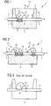
- FIG. 1 it is a semiconductor detector component 1 with a housing body 2 made of thermoplastic material, here for example PPA, which is sprayed around -one electrical lead frame 9 made of metal.
- the lead frame 9 is provided with a silver coating 7 and partially enclosed by the housing body 2.
- the housing body 2 is injection-molded or injection-molded, for example.
- a detector chip 31 is applied with a silver-filled conductive adhesive 3.
- the thermoplastic material of the housing body 2 with platelet-like filler particles 6 of kaolin average size, for example, about 3 ⁇ m) are added, which prevent migration of silver from the coating 7 of the lead frame 9 and from the conductive adhesive 3 or at least severely hamper.
- silver another metal, which tends to migrate in plastic, can also be located on the lead frame 9 and / or in the conductive adhesive 3, such as e.g. Nickel or copper.
- kaolin filler another powder, preferably a non-metallic powder, such as a ceramic or mineral powder may be used.
- a non-metallic powder such as a ceramic or mineral powder
- glass beads as filler particles 6 is possible.
- the plastic which prevent migration of metal in the plastic of the housing body 2
- other materials may be present in the plastic, such as TiO 2 or similar scattering particles, which contribute to the housing body being opaque and having a high diffuse reflectance for example, has 80%.
- the housing body can, as mentioned above, consist of polyphthalamide, but also of any other thermoplastic material, which has the necessary properties for a housing body 2, such as mechanical and thermal stability.
- the lead frame 9 has two or more external terminal parts 4, 5, which protrude from the housing body 2.
- the housing body 2 has a reflector recess 14, in which the chip 31 is arranged.
- the reflector recess 14 is filled with a radiation-permeable window part 13.
- the embodiment according to FIG. 2 differs from the embodiment described above in particular in that the component has two semiconductor chips, for example a detector chip and an emitter chip, two emitter chips or two detector chips, which are at greatly different potential during operation of the device.
- the component has two semiconductor chips, for example a detector chip and an emitter chip, two emitter chips or two detector chips, which are at greatly different potential during operation of the device.
- electrical fields 12,22 prevail between the terminals of the leadframe, which would accelerate metal migration in the housing body. Also in this electric field, metal migration is prevented or at least sufficiently hindered by the platelet-like kaolin filler particles 6 in a non-invention embodiment.
- the device according to FIG. 3 has a conventional housing body containing no filler particles according to the invention, but glass fibers.
- a detector chip 31 is attached to the lead frame 9 with silver-containing conductive adhesive 3 and the conductive adhesive is in direct contact with the housing body 2. After a certain period of operation, an electrically conductive path 10 can form in the housing body 2 due to silver migration between the two separate lead frame parts. which can lead in the worst case to a total failure of the device.
- the invention is of course not limited to the specific embodiments described. In particular, it can be used for housing body of different geometry.
- An optoelectronic device with a housing body according to the invention in a simple manner substantially prevents the migration of metal in the housing body and can avoid the use of expensive contact material such as gold.
Landscapes
- Compositions Of Macromolecular Compounds (AREA)
- Led Device Packages (AREA)
- Light Receiving Elements (AREA)
- Casings For Electric Apparatus (AREA)
- Structures Or Materials For Encapsulating Or Coating Semiconductor Devices Or Solid State Devices (AREA)
Claims (10)
- Composant optoélectronique (1) avec- un corps de boîtier (2) constitué au moins partiellement en matériau plastique,- au moins une puce (31) émettant et / ou recevant un rayonnement électromagnétique, attachée sur au moins une partie de support de puce (8) d'un cadre conducteur (9), ledit cadre conducteur (9) comportant au moins deux pièces de connexion électrique externes (4, 5) connectées électriquement de manière conductrice à la puce (31), dans lequel- la partie de support de puce (8) et les sous-régions des pièces de connexion électrique externes (4, 5) sont entourées par le corps de boîtier (2) d'où les pièces de connexion électrique externes (4, 5) font saillie,- le corps de boîtier (2) présente un évidement (14) dans lequel la puce (31) est agencée sur la partie de support de puce (8),caractérisé en ce que- le matériau plastique du corps de boîtier (2) est mélangé avec des particules de charge (6), les particules de charge (6) ayant une forme sphérique, et- les particules de charge empêchent une migration d'argent dans un champ électrique (22, 12) entre les pièces de connexion électrique externes (4, 5) dans le matériau plastique.
- Composant selon la revendication 1,
caractérisé en ce que
la puce (31) est une puce à photo-détecteur à semi-conducteur. - Composant selon la revendication 1,
caractérisé en ce que
dans l'évidement (14) est disposée une pluralité de puces (31) sur plusieurs parties de support de puce (8), dont au moins une est une puce à photo-détecteur à semi-conducteur. - Composant selon la revendication 1,
caractérisé en ce que
dans l'évidement (14) est disposée une pluralité de puces émettant des radiations (31) sur plusieurs parties de support de puces (8). - Composant selon l'une des revendications 1 à 4,
caractérisé en ce que
le matériau plastique comprend un matériau thermoplastique, en particulier du polyphtalamide (PPA). - Composant selon l'une des revendications 1 à 5,
caractérisé en ce que
le corps de boîtier (2) est adapté au cadre électriquement conducteur (9) par moulage par injection ou par transfert. - Composant selon l'une des revendications 1 à 6,
caractérisé en ce que
le cadre électriquement conducteur (9) présente une surface métallique (7) ou un revêtement métallique contenant de l'argent. - Composant selon l'une des revendications 1 à 7,
caractérisé en ce que
une colle conductrice chargée de métal (3) contenant de l'argent est disposée sur au moins l'une des pièces de connexion électrique. - Composant selon l'une des revendications 1 à 8,
caractérisé en ce que des billes de verre sont utilisées en tant que particules de charge (6). - Composant selon l'une des revendications 1 à 9,
caractérisé en ce que
des propriétés mécaniques du corps de boîtier (2) sont ajustées délibérément grâce aux particules de charge (6).
Applications Claiming Priority (5)
| Application Number | Priority Date | Filing Date | Title |
|---|---|---|---|
| DE10310619 | 2003-03-10 | ||
| DE10310619 | 2003-03-10 | ||
| DE10310844 | 2003-03-11 | ||
| DE10310844.0A DE10310844B4 (de) | 2003-03-10 | 2003-03-11 | Optoelektronisches Bauelement mit einem Gehäusekörper aus Kunststoff |
| PCT/DE2004/000271 WO2004081972A2 (fr) | 2003-03-10 | 2004-02-13 | Boitier, composant optoelectronique pourvu d'un tel boitier et matiere plastique pour boitier |
Publications (2)
| Publication Number | Publication Date |
|---|---|
| EP1604385A2 EP1604385A2 (fr) | 2005-12-14 |
| EP1604385B1 true EP1604385B1 (fr) | 2019-12-11 |
Family
ID=32991925
Family Applications (1)
| Application Number | Title | Priority Date | Filing Date |
|---|---|---|---|
| EP04710788.3A Expired - Lifetime EP1604385B1 (fr) | 2003-03-10 | 2004-02-13 | Composant optoélectronique avec un corps de boitier en matière plastique |
Country Status (3)
| Country | Link |
|---|---|
| EP (1) | EP1604385B1 (fr) |
| TW (1) | TWI244168B (fr) |
| WO (1) | WO2004081972A2 (fr) |
Families Citing this family (2)
| Publication number | Priority date | Publication date | Assignee | Title |
|---|---|---|---|---|
| DE102008025491A1 (de) | 2008-05-28 | 2009-12-03 | Osram Opto Semiconductors Gmbh | Optoelektronisches Halbleiterbauteil und Leiterplatte |
| US9806711B1 (en) * | 2016-09-28 | 2017-10-31 | International Business Machines Corporation | Quantum limited josephson amplifier with spatial separation between spectrally degenerate signal and idler modes |
Citations (3)
| Publication number | Priority date | Publication date | Assignee | Title |
|---|---|---|---|---|
| US20020089047A1 (en) * | 1997-07-29 | 2002-07-11 | Osram Opto Semiconductors Gmbh & Co. Ohg | Surface-mountable light-emitting diode structural element |
| EP1249874A2 (fr) * | 2001-04-09 | 2002-10-16 | Kabushiki Kaisha Toshiba | Dispositif émetteur de lumière |
| DE10117890A1 (de) * | 2001-04-10 | 2002-10-24 | Osram Opto Semiconductors Gmbh | Verfahren zum Herstellen eines strahlungsempfangenden und/oder emittierenden Halbleiterbauelements und strahlungsempfangendes und/oder -emittierendes Halbleiterbauelement |
Family Cites Families (7)
| Publication number | Priority date | Publication date | Assignee | Title |
|---|---|---|---|---|
| JPH0612829B2 (ja) * | 1984-04-24 | 1994-02-16 | 株式会社東芝 | 半導体装置 |
| CA1331245C (fr) * | 1987-12-21 | 1994-08-02 | Carol Ann Latham | Matieres composites ceramique/polymeres thermiquement conductrices |
| JPH10190173A (ja) * | 1996-12-25 | 1998-07-21 | Kyocera Corp | 配線基板 |
| JP2001335708A (ja) * | 2000-05-26 | 2001-12-04 | Matsushita Electric Works Ltd | 熱可塑性樹脂組成物、その製造方法、並びに半導体素子収納用パッケージ |
| JP2001339143A (ja) * | 2000-05-29 | 2001-12-07 | Kyocera Corp | 配線基板 |
| WO2001096458A1 (fr) * | 2000-06-16 | 2001-12-20 | Siemens Aktiengesellschaft | Matiere de charge pour plastiques thermoconducteurs, plastique thermoconducteur et procede de fabrication |
| JP2003092379A (ja) * | 2001-09-18 | 2003-03-28 | Hitachi Ltd | 半導体装置 |
-
2004
- 2004-02-13 EP EP04710788.3A patent/EP1604385B1/fr not_active Expired - Lifetime
- 2004-02-13 WO PCT/DE2004/000271 patent/WO2004081972A2/fr not_active Ceased
- 2004-03-01 TW TW93105284A patent/TWI244168B/zh not_active IP Right Cessation
Patent Citations (3)
| Publication number | Priority date | Publication date | Assignee | Title |
|---|---|---|---|---|
| US20020089047A1 (en) * | 1997-07-29 | 2002-07-11 | Osram Opto Semiconductors Gmbh & Co. Ohg | Surface-mountable light-emitting diode structural element |
| EP1249874A2 (fr) * | 2001-04-09 | 2002-10-16 | Kabushiki Kaisha Toshiba | Dispositif émetteur de lumière |
| DE10117890A1 (de) * | 2001-04-10 | 2002-10-24 | Osram Opto Semiconductors Gmbh | Verfahren zum Herstellen eines strahlungsempfangenden und/oder emittierenden Halbleiterbauelements und strahlungsempfangendes und/oder -emittierendes Halbleiterbauelement |
Also Published As
| Publication number | Publication date |
|---|---|
| WO2004081972A2 (fr) | 2004-09-23 |
| WO2004081972A3 (fr) | 2005-04-28 |
| TWI244168B (en) | 2005-11-21 |
| TW200423314A (en) | 2004-11-01 |
| EP1604385A2 (fr) | 2005-12-14 |
Similar Documents
| Publication | Publication Date | Title |
|---|---|---|
| EP2267798B1 (fr) | Dispositif opto-électronique | |
| DE19829197C2 (de) | Strahlungsaussendendes und/oder -empfangendes Bauelement | |
| EP2062301B1 (fr) | Boîtier pour composant optoélectronique et disposition d'un composant optoélectronique dans le boîtier | |
| WO2008040324A1 (fr) | boîtier pour composant optoélectronique, composant optoélectronique et procédé de fabrication d'un boîtier pour composant optoélectronique | |
| DE10243247A1 (de) | Leadframe-basiertes Bauelement-Gehäuse, Leadframe-Band, oberflächenmontierbares elektronisches Bauelement und Verfahren zur Herstellung | |
| EP2550684A1 (fr) | Composant semi-conducteur émetteur de rayonnement | |
| WO2011161183A1 (fr) | Composant semi-conducteur optoélectronique | |
| EP2593974A2 (fr) | Dispositif support pour une puce semi-conductrice, composant électronique comportant un dispositif support et composant optoélectronique comportant un dispositif support | |
| DE102019119371A1 (de) | Bauteil und verfahren zur herstellung eines bauteils | |
| EP2452547A1 (fr) | Composant électronique | |
| DE102022116908A1 (de) | Halbleitervorrichtung | |
| DE10310844B4 (de) | Optoelektronisches Bauelement mit einem Gehäusekörper aus Kunststoff | |
| EP1717871A2 (fr) | Composant optoélectronique montable en surface | |
| DE102010003321A1 (de) | Optoelektronisches Bauelement | |
| WO2004081972A2 (fr) | Boitier, composant optoelectronique pourvu d'un tel boitier et matiere plastique pour boitier | |
| DE68911441T2 (de) | Anordnung mit einer elektronischen Schaltung, montiert auf einem biegsamen Träger, geschützt gegen elektrostatische Entladungen, und biegsame Karte mit dieser Anordnung. | |
| WO2011141383A1 (fr) | Couche réfléchissante en argent résistant à la corrosion pour un composant optoélectronique, composant correspondant et procédé de fabrication | |
| DE102016103354A1 (de) | Optoelektronisches bauteil mit einem leiterrahmen | |
| DE102022116914A1 (de) | Halbleitervorrichtung | |
| DE102009023854B4 (de) | Optoelektronisches Halbleiterbauelement | |
| DE102017101399A1 (de) | Sensoranordnung | |
| EP2641278A1 (fr) | Composant semi-conducteur optoélectronique | |
| DE102011107958B4 (de) | Überschlagsschutz für eine Anordnung eines Halbleiterbauelements auf einem Substrat | |
| WO2014005572A2 (fr) | Supports pour composants électriques avec mise en contact auto-étanche | |
| DE102022116911A1 (de) | Anschlusselement und halbleitervorrichtung |
Legal Events
| Date | Code | Title | Description |
|---|---|---|---|
| PUAI | Public reference made under article 153(3) epc to a published international application that has entered the european phase |
Free format text: ORIGINAL CODE: 0009012 |
|
| 17P | Request for examination filed |
Effective date: 20051007 |
|
| AK | Designated contracting states |
Kind code of ref document: A2 Designated state(s): AT BE BG CH CY CZ DE DK EE ES FI FR GB GR HU IE IT LI LU MC NL PT RO SE SI SK TR |
|
| AX | Request for extension of the european patent |
Extension state: AL LT LV MK |
|
| RAP1 | Party data changed (applicant data changed or rights of an application transferred) |
Owner name: OSRAM OPTO SEMICONDUCTORS GMBH |
|
| DAX | Request for extension of the european patent (deleted) | ||
| RBV | Designated contracting states (corrected) |
Designated state(s): DE |
|
| RIN1 | Information on inventor provided before grant (corrected) |
Inventor name: KRAEUTER, GERTRUD Inventor name: BRUNNER, HERBERT Inventor name: ZEILER, MARKUS Inventor name: HOEFER, THOMAS |
|
| 17Q | First examination report despatched |
Effective date: 20060223 |
|
| RAP1 | Party data changed (applicant data changed or rights of an application transferred) |
Owner name: OSRAM OPTO SEMICONDUCTORS GMBH |
|
| RAP1 | Party data changed (applicant data changed or rights of an application transferred) |
Owner name: OSRAM OPTO SEMICONDUCTORS GMBH |
|
| RIC1 | Information provided on ipc code assigned before grant |
Ipc: H01L 21/00 20060101AFI20041001BHEP |
|
| GRAP | Despatch of communication of intention to grant a patent |
Free format text: ORIGINAL CODE: EPIDOSNIGR1 |
|
| RIC1 | Information provided on ipc code assigned before grant |
Ipc: H01L 23/057 20060101ALI20190514BHEP Ipc: H01L 33/62 20100101ALN20190514BHEP Ipc: H01L 25/16 20060101ALN20190514BHEP Ipc: H01L 33/48 20100101ALI20190514BHEP Ipc: H01L 31/0203 20140101AFI20190514BHEP Ipc: H01L 23/00 20060101ALI20190514BHEP |
|
| RIC1 | Information provided on ipc code assigned before grant |
Ipc: H01L 31/0203 20140101AFI20190524BHEP Ipc: H01L 33/48 20100101ALI20190524BHEP Ipc: H01L 23/057 20060101ALI20190524BHEP Ipc: H01L 23/00 20060101ALI20190524BHEP Ipc: H01L 33/62 20100101ALN20190524BHEP Ipc: H01L 25/16 20060101ALN20190524BHEP |
|
| INTG | Intention to grant announced |
Effective date: 20190617 |
|
| RAP1 | Party data changed (applicant data changed or rights of an application transferred) |
Owner name: OSRAM OPTO SEMICONDUCTORS GMBH |
|
| GRAJ | Information related to disapproval of communication of intention to grant by the applicant or resumption of examination proceedings by the epo deleted |
Free format text: ORIGINAL CODE: EPIDOSDIGR1 |
|
| REG | Reference to a national code |
Ref country code: DE Ref legal event code: R079 Ref document number: 502004015843 Country of ref document: DE Free format text: PREVIOUS MAIN CLASS: H01L0021000000 Ipc: H01L0031020300 |
|
| GRAR | Information related to intention to grant a patent recorded |
Free format text: ORIGINAL CODE: EPIDOSNIGR71 |
|
| GRAS | Grant fee paid |
Free format text: ORIGINAL CODE: EPIDOSNIGR3 |
|
| GRAA | (expected) grant |
Free format text: ORIGINAL CODE: 0009210 |
|
| INTC | Intention to grant announced (deleted) | ||
| RIC1 | Information provided on ipc code assigned before grant |
Ipc: H01L 25/16 20060101ALN20191021BHEP Ipc: H01L 23/00 20060101ALI20191021BHEP Ipc: H01L 31/0203 20140101AFI20191021BHEP Ipc: H01L 33/48 20100101ALI20191021BHEP Ipc: H01L 23/057 20060101ALI20191021BHEP Ipc: H01L 33/62 20100101ALN20191021BHEP |
|
| AK | Designated contracting states |
Kind code of ref document: B1 Designated state(s): DE |
|
| INTG | Intention to grant announced |
Effective date: 20191104 |
|
| REG | Reference to a national code |
Ref country code: DE Ref legal event code: R096 Ref document number: 502004015843 Country of ref document: DE |
|
| REG | Reference to a national code |
Ref country code: DE Ref legal event code: R097 Ref document number: 502004015843 Country of ref document: DE |
|
| PLBE | No opposition filed within time limit |
Free format text: ORIGINAL CODE: 0009261 |
|
| STAA | Information on the status of an ep patent application or granted ep patent |
Free format text: STATUS: NO OPPOSITION FILED WITHIN TIME LIMIT |
|
| 26N | No opposition filed |
Effective date: 20200914 |
|
| REG | Reference to a national code |
Ref country code: DE Ref legal event code: R082 Ref document number: 502004015843 Country of ref document: DE Representative=s name: SCHEELE JAEGER WETZEL PATENTANWAELTE PARTNERSC, DE |
|
| PGFP | Annual fee paid to national office [announced via postgrant information from national office to epo] |
Ref country code: DE Payment date: 20230216 Year of fee payment: 20 |
|
| P01 | Opt-out of the competence of the unified patent court (upc) registered |
Effective date: 20230825 |
|
| REG | Reference to a national code |
Ref country code: DE Ref legal event code: R071 Ref document number: 502004015843 Country of ref document: DE |