EP1605310A2 - Belichtungssystem und Mustererzeugungsverfahren - Google Patents
Belichtungssystem und Mustererzeugungsverfahren Download PDFInfo
- Publication number
- EP1605310A2 EP1605310A2 EP05012154A EP05012154A EP1605310A2 EP 1605310 A2 EP1605310 A2 EP 1605310A2 EP 05012154 A EP05012154 A EP 05012154A EP 05012154 A EP05012154 A EP 05012154A EP 1605310 A2 EP1605310 A2 EP 1605310A2
- Authority
- EP
- European Patent Office
- Prior art keywords
- resist film
- exposure
- pattern
- formation method
- laser
- Prior art date
- Legal status (The legal status is an assumption and is not a legal conclusion. Google has not performed a legal analysis and makes no representation as to the accuracy of the status listed.)
- Granted
Links
Images


Classifications
-
- G—PHYSICS
- G03—PHOTOGRAPHY; CINEMATOGRAPHY; ANALOGOUS TECHNIQUES USING WAVES OTHER THAN OPTICAL WAVES; ELECTROGRAPHY; HOLOGRAPHY
- G03F—PHOTOMECHANICAL PRODUCTION OF TEXTURED OR PATTERNED SURFACES, e.g. FOR PRINTING, FOR PROCESSING OF SEMICONDUCTOR DEVICES; MATERIALS THEREFOR; ORIGINALS THEREFOR; APPARATUS SPECIALLY ADAPTED THEREFOR
- G03F7/00—Photomechanical, e.g. photolithographic, production of textured or patterned surfaces, e.g. printing surfaces; Materials therefor, e.g. comprising photoresists; Apparatus specially adapted therefor
- G03F7/70—Microphotolithographic exposure; Apparatus therefor
- G03F7/70216—Mask projection systems
- G03F7/70341—Details of immersion lithography aspects, e.g. exposure media or control of immersion liquid supply
-
- G—PHYSICS
- G03—PHOTOGRAPHY; CINEMATOGRAPHY; ANALOGOUS TECHNIQUES USING WAVES OTHER THAN OPTICAL WAVES; ELECTROGRAPHY; HOLOGRAPHY
- G03F—PHOTOMECHANICAL PRODUCTION OF TEXTURED OR PATTERNED SURFACES, e.g. FOR PRINTING, FOR PROCESSING OF SEMICONDUCTOR DEVICES; MATERIALS THEREFOR; ORIGINALS THEREFOR; APPARATUS SPECIALLY ADAPTED THEREFOR
- G03F7/00—Photomechanical, e.g. photolithographic, production of textured or patterned surfaces, e.g. printing surfaces; Materials therefor, e.g. comprising photoresists; Apparatus specially adapted therefor
- G03F7/16—Coating processes; Apparatus therefor
- G03F7/168—Finishing the coated layer, e.g. drying, baking, soaking
-
- G—PHYSICS
- G03—PHOTOGRAPHY; CINEMATOGRAPHY; ANALOGOUS TECHNIQUES USING WAVES OTHER THAN OPTICAL WAVES; ELECTROGRAPHY; HOLOGRAPHY
- G03F—PHOTOMECHANICAL PRODUCTION OF TEXTURED OR PATTERNED SURFACES, e.g. FOR PRINTING, FOR PROCESSING OF SEMICONDUCTOR DEVICES; MATERIALS THEREFOR; ORIGINALS THEREFOR; APPARATUS SPECIALLY ADAPTED THEREFOR
- G03F7/00—Photomechanical, e.g. photolithographic, production of textured or patterned surfaces, e.g. printing surfaces; Materials therefor, e.g. comprising photoresists; Apparatus specially adapted therefor
- G03F7/20—Exposure; Apparatus therefor
- G03F7/2041—Exposure; Apparatus therefor in the presence of a fluid, e.g. immersion; using fluid cooling means
-
- G—PHYSICS
- G03—PHOTOGRAPHY; CINEMATOGRAPHY; ANALOGOUS TECHNIQUES USING WAVES OTHER THAN OPTICAL WAVES; ELECTROGRAPHY; HOLOGRAPHY
- G03F—PHOTOMECHANICAL PRODUCTION OF TEXTURED OR PATTERNED SURFACES, e.g. FOR PRINTING, FOR PROCESSING OF SEMICONDUCTOR DEVICES; MATERIALS THEREFOR; ORIGINALS THEREFOR; APPARATUS SPECIALLY ADAPTED THEREFOR
- G03F7/00—Photomechanical, e.g. photolithographic, production of textured or patterned surfaces, e.g. printing surfaces; Materials therefor, e.g. comprising photoresists; Apparatus specially adapted therefor
- G03F7/70—Microphotolithographic exposure; Apparatus therefor
- G03F7/708—Construction of apparatus, e.g. environment aspects, hygiene aspects or materials
- G03F7/70991—Connection with other apparatus, e.g. multiple exposure stations, particular arrangement of exposure apparatus and pre-exposure and/or post-exposure apparatus; Shared apparatus, e.g. having shared radiation source, shared mask or workpiece stage, shared base-plate; Utilities, e.g. cable, pipe or wireless arrangements for data, power, fluids or vacuum
-
- G—PHYSICS
- G03—PHOTOGRAPHY; CINEMATOGRAPHY; ANALOGOUS TECHNIQUES USING WAVES OTHER THAN OPTICAL WAVES; ELECTROGRAPHY; HOLOGRAPHY
- G03F—PHOTOMECHANICAL PRODUCTION OF TEXTURED OR PATTERNED SURFACES, e.g. FOR PRINTING, FOR PROCESSING OF SEMICONDUCTOR DEVICES; MATERIALS THEREFOR; ORIGINALS THEREFOR; APPARATUS SPECIALLY ADAPTED THEREFOR
- G03F7/00—Photomechanical, e.g. photolithographic, production of textured or patterned surfaces, e.g. printing surfaces; Materials therefor, e.g. comprising photoresists; Apparatus specially adapted therefor
- G03F7/004—Photosensitive materials
- G03F7/039—Macromolecular compounds which are photodegradable, e.g. positive electron resists
- G03F7/0392—Macromolecular compounds which are photodegradable, e.g. positive electron resists the macromolecular compound being present in a chemically amplified positive photoresist composition
- G03F7/0395—Macromolecular compounds which are photodegradable, e.g. positive electron resists the macromolecular compound being present in a chemically amplified positive photoresist composition the macromolecular compound having a backbone with alicyclic moieties
Definitions
- the present invention relates to an exposure system for use in fabrication process or the like for semiconductor devices and a pattern formation method using the same.
- immersion lithography has been recently proposed for realizing further refinement of patterns by using conventional exposing light (for example, see M. Switkes and M. Rothschild, "Immersion lithography at 157 nm", J. Vac. Sci. Technol., Vol. B19, p. 2353 (2001)).
- FIGS. 9A through 9D a conventional pattern formation method employing the immersion lithography will be described with reference to FIGS. 9A through 9D .
- pattern exposure is carried out by irradiating the resist film 2 with exposing light 4 of ArF excimer laser with NA of 0.68 through a mask.
- the resist film 2 is baked with a hot plate at a temperature of 105°C for 60 seconds, and the resultant resist film is developed with a tetramethylammonium hydroxide developer in a concentration of 0.26 N. In this manner, a resist pattern 2a made of an unexposed portion of the resist film 2 is formed as shown in FIG. 9D.
- the resist pattern 2a formed by the conventional pattern formation method employing the immersion lithography is in a defective shape.
- the present inventors have variously examined the reason why the resist pattern formed by the conventional immersion lithography is in a defective shape, resulting in finding that the defective shape of the pattern is caused because particles adhered onto the surface of the resist film 2 float into the immersion liquid 3 so as to scatter the exposing light 4 .
- the resist pattern is formed in a defective shape when the exposure is performed through the liquid including such particles, and when the resist pattern in such a defective shape is used for etching, a pattern made of an etched film is also in a defective shape.
- the productivity and the yield of the fabrication process for semiconductor devices are disadvantageously lowered.
- an object of the invention is forming a resist pattern in a good shape through lithography, and more particularly, through the immersion lithography.
- the surface of a resist film is cleaned or dissolved before exposure, so as to remove particles remaining on the surface of the resist film.
- the immersion exposure a liquid such as water is filled between a resist film formed on a wafer and an exposure lens so as to increase the substantial value of the numerical aperture (NA) as described above. Accordingly, if particles remain on the surface of the resist film, the remaining particles start to float into the liquid when the liquid is provided on the resist film.
- NA numerical aperture
- the resist film in direct contact with the immersion liquid during the exposure, and therefore, the particles are easily released from the surface of the resist film so as to float into the liquid, resulting in scattering the exposing light in arbitrary positions. Furthermore, there arises another problem that the floating particles are adhered onto the exposure lens whose accuracy is significant. In other words, it is apprehended in the immersion exposure that one particle degrades exposure accuracy in a plurality of positions. Accordingly, adhesion of particles onto the resist film is a very serious problem as compared with that in the dry exposure.
- a resist pattern can be formed in a good shape through exposure and development by removing particles, before the exposure, by cleaning or dissolving the surface of a resist film formed on a wafer.
- the first exposure system of this invention includes: a coating unit for forming a resist film on a substrate; a cleaning unit for cleaning a surface of the resist film; and an exposure unit for performing pattern exposure with a liquid provided between the resist film and an exposure lens, wherein the cleaning unit is placed between the coating unit and the exposure unit.
- the immersion exposure is performed by the exposure unit for performing the pattern exposure with the liquid provided. Therefore, pattern failures derived from particles can be prevented in the immersion exposure.
- the second exposure system of this invention includes: a coating unit for forming a resist film on a substrate; a cleaning unit for cleaning a surface of the resist film; and an exposure unit for performing pattern exposure, wherein the cleaning unit is placed between the coating unit and the exposure unit.
- the dry exposure is performed by the exposure unit for performing the pattern exposure. Therefore, pattern failures derived from particles can be prevented.
- the cleaning unit and the exposure unit are placed in a chamber, a plurality of arms each having a wafer holding head are set in the chamber, and one of the plurality of arms is placed in the cleaning unit while another one of the plurality of arms is placed in the exposure unit.
- the resist film can be cleaned on the first stage and the wafer having the resist film cleaned can be moved to the second stage for performing the pattern exposure within one exposure system. Therefore, even when the cleaning process is additionally carried out, the throughput of the exposure is not largely degraded.
- the first pattern formation method of this invention includes the steps of forming a resist film on a substrate; cleaning a surface of the resist film; performing pattern exposure by selectively irradiating the resist film with exposing light with a liquid provided on the resist film whose surface has been cleaned; and forming a resist pattern by developing the resist film after the pattern exposure.
- the second pattern formation method of this invention includes the steps of forming a resist film on a substrate; dissolving a surface of the resist film; performing pattern exposure by selectively irradiating the resist film with exposing light with a liquid provided on the resist film whose surface has been dissolved; and forming a resist pattern by developing the resist film after the pattern exposure.
- the third pattern formation method of this invention includes the steps of forming a resist film on a substrate; cleaning a surface of the resist film; performing pattern exposure by selectively irradiating, with exposing light, the resist film whose surface has been cleaned; and forming a resist pattern by developing the resist film after the pattern exposure.
- the fourth pattern formation method of this invention includes the steps of forming a resist film on a substrate; dissolving a surface of the resist film; performing pattern exposure by selectively irradiating, with exposing light, the resist film whose surface has been dissolved; and forming a resist pattern by developing the resist film after the pattern exposure.
- the cleaning or dissolving step performed on the resist film before the exposure may be carried out inside or outside of the exposure system in any of the first through fourth pattern formation methods.
- the surface of the resist film may be cleaned with water or ozone water.
- the surface of the resist film is dissolved in an alkaline aqueous solution.
- the thickness of the resist film thus removed is approximately 0.1 nm through 10 nm and preferably several nm.
- the alkaline aqueous solution may be a developer used for developing the resist film or a diluted developer obtained by diluting the developer.
- the diluted developer used in this case preferably has a concentration not lower than 0.01 N and lower than 0.26 N, which does not limit the invention.
- the liquid can be water or perfluoropolyether.
- the exposing light can be KrF excimer laser, ArF excimer laser, F 2 laser, Xe 2 laser, Ar 2 laser or ArKr laser.
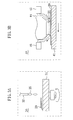
- FIG. 1 schematically shows the cross-sectional structure of a principal part of an exposure system according to Embodiment 1 of the invention.
- the exposure system 10 of Embodiment 1 is provided in a chamber 11 .
- it includes a cleaning unit 30 for cleaning a resist film (not shown) formed on a principal surface of a wafer 20 and a pattern exposure unit 40 for performing pattern exposure on the cleaned resist film.
- a surface plate 12 for supporting a stage where the wafer 20 is placed is provided in a lower portion of the chamber 11 .
- the stage includes twin stages of, for example, a first movable stage 31 and a second movable stage 41 .
- the first movable stage 31 and the second movable stage 41 are spaced from each other on the surface plate 12 so as to be individually moved by the surface plate 12 .
- the cleaning unit 30 includes, above the first movable stage 31 , a cleaning fluid supplying nozzle 32 for cleaning the surface of the resist film on the wafer 20 with a cleaning fluid 25 .
- the pattern exposure unit 40 includes an illumination optical system 42 including a light source for the pattern exposure and a projection lens 44 provided below the illumination optical system 42 .
- the projection lens 44 projects, through an immersion liquid 26 onto the resist film, exposing light emitted from the illumination optical system 42 and entering through a mask (reticle) 43 having a design pattern to be transferred onto the resist film.
- the second movable stage 41 for holding the wafer 20 is disposed below the projection lens 44 disposed. At this point, the projection lens 44 is held so as to be in contact with the surface of the liquid 26 provided on the resist film on the wafer 20 during the exposure.
- FIG. 2A simply shows the units included in the exposure system.
- a resist film is applied on a principal surface of the wafer in a general coating unit 50, and the resultant wafer having the resist film is transferred to the exposure system 10 .
- the wafer having been transferred to the cleaning unit 30 of the exposure system 10 is cleaned on the surface of the resist film in the cleaning unit 30 .
- the wafer having the surface of the resist film cleaned in the cleaning unit 30 of the exposure system 10 is transferred to the pattern exposure unit 40 of the exposure system 10 , where the immersion exposure is performed.
- FIG. 2B the illumination optical system 42 , the projection lens 44 and the like of the pattern exposure unit 40 are omitted.
- a conveyer 60 capable of conveying the wafer 20 between the cleaning unit 30 and the pattern exposure unit 40 is provided between the cleaning unit 30 and the pattern exposure unit 40 .
- the conveyer 60 includes arm portions 61 and wafer holding heads 62 .
- the arm portions 61 a plurality of arms having their center at the center of the exposure system are radially provided.
- the arm portions 61 include two arms parallel to the principal surface of the surface plate 12 and crossing each other on a crossing part.
- the arm portions 61 are rotatable with the crossing part set as the rotation axis and in parallel to the principal surface of the surface plate 12 .
- the four arm portions 61 composed of the two crossing arms are held so as to have an angle between the adjacent arm portions of approximately 90°.
- the wafer holding head 62 is provided on each tip of the arm portions 61.
- the wafer 20 having been transferred after the film deposition is held to be adsorbed on the wafer holding head 62 by using the atmospheric pressure or the like.
- the wafer 20 having been transferred from the coating unit 50 on which the resist film has been applied is held on one wafer holding head 62 of the conveyer 60 to be moved to the first movable stage 31 .
- the wafer 20 having been moved to the first movable stage 31 is cleaned for particles adhered onto the resist film with the cleaning fluid 25 supplied from the cleaning fluid supplying nozzle 32 .
- the cleaning fluid 25 supplied from the cleaning fluid supplying nozzle 32 supplied from the cleaning fluid supplying nozzle 32 .
- the whole principal surface of the wafer 20 is not exposed at one time but the wafer 20 is divided into a plurality of exposure regions 20a and each of the exposure regions 20a is exposed. Accordingly, in the wafer 20 having been moved to the second movable stage 41 of the pattern exposure unit 40 , a desired design pattern is successively exposed on each of the exposure regions 20a , and then, the resultant wafer 20 is transferred to a developing unit (not shown) for subsequent processing.
- the wafer 20 having a resist film applied thereon is held on the first movable stage 31 of the cleaning unit 30 as shown in FIG. 3A.
- the cleaning fluid 25 is dropped on the resist film from the cleaning fluid supplying nozzle 32 provided above the first movable stage 31.
- the cleaning fluid 25 for example, ozone water obtained by dissolving ozone (O 3 ) in water (pure water) can be used.
- a method for supplying the cleaning fluid in a smaller particle size, namely, for spraying the cleaning fluid may be employed. This is because the surface of the resist film may be harmfully affected by the impact of drops when the cleaning fluid is dropped on the resist film in the form of drops.
- a supply port 45 for supplying the immersion liquid 26 onto the wafer 20 and a discharge port 46 for discharging the supplied liquid 26 from above the wafer 20 are provided on the side of the projection lens 44 .
- the immersion liquid 26 is supplied from the supply port 45 to a region that corresponds to one exposure region 20a of the wafer 20 and is sandwiched between the resist film and the projection lens 44 .
- the exposure region 20a is subjected to desired pattern exposure with the liquid 26 provided between the resist film and the projection lens 44 , and then, the liquid 26 is discharged from the discharge port 46 .
- the liquid 26 is supplied onto this exposure region 20a , which is then subjected to the desired pattern exposure. In this manner, all the exposure regions 20a on the wafer 20 are successively exposed.
- the operations for supplying the immersion liquid 26 , performing the exposure and discharging the liquid 26 are preferably continuously performed.
- the surface of the resist film formed on the wafer 20 is cleaned immediately before the pattern exposure in the cleaning unit 30 provided in the chamber 11 with high cleanness, so as to remove particles adhered onto the resist film. Therefore, the pattern exposure is not affected by the particles, so that the resist film can be formed into a resist pattern in a good shape.
- the immersion liquid 26 is supplied onto each of the exposure regions 20a on the wafer 20 by employing what is called the dropping method in Embodiment 1, which does not limit the invention. Instead, the invention is effective when what is called the pooling method in which the wafer 20 itself is immersed in the liquid is employed.
- the cleaning unit 30 and the pattern exposure unit 40 are provided in the chamber 11 , but the cleaning unit 30 may be provided outside the exposure system 10 . Furthermore, if the environment (atmosphere) in which the exposure system 10 is installed has sufficiently high cleanness, the chamber 11 is not always necessary.
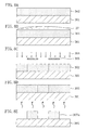
- FIGS. 4A through 4E a pattern formation method using the exposure system having the aforementioned structure will be described with reference to FIGS. 4A through 4E .
- the aforementioned chemically amplified resist material is applied on a wafer 20 so as to form a resist film 21 with a thickness of 0.35 ⁇ m.
- the resist film 21 is cleaned with a cleaning fluid 24 of, for example, water in the cleaning unit 30 of the exposure system 10 of FIG. 1.
- pattern exposure is carried out by irradiating the resist film 21 through a mask (not shown) with exposing light 47 of ArF excimer laser with NA of 0.68.
- the resist film 21 is baked with a hot plate at a temperature of 105°C for 60 seconds, and thereafter, the resultant resist film 21 is developed with a tetramethylammonium hydroxide developer in a concentration of 0.26 N. In this manner, a resist pattern 21a made of an unexposed portion of the resist film 21 and having a line width of 0.09 ⁇ m is formed in a good shape as shown in FIG. 4E .
- the surface of the resist film 21 formed on the wafer 20 is cleaned with the cleaning fluid 25 before the pattern exposure so as to remove particles adhered onto the surface of the resist film 21 . Accordingly, the pattern exposure is not affected by the particles, so that the resist film 21 can be formed into the resist pattern 21a in a good shape.
- the aforementioned chemically amplified resist material is applied on a wafer 101 so as to form a resist film 102 with a thickness of 0.35 ⁇ m.
- the surface of the resist film 102 is dissolved in an alkaline aqueous solution 27 of, for example, a tetramethylammonium hydroxide developer in a concentration of 0.1 N.
- an alkaline aqueous solution 27 of, for example, a tetramethylammonium hydroxide developer in a concentration of 0.1 N.
- a surface portion of the resist film 102 is removed by the alkaline aqueous solution 27 .
- the thickness of the surface portion of the resist film 102 removed at this point depends upon the concentration of the alkaline aqueous solution and the time for allowing the resist film to be in contact with the alkaline aqueous solution, and is approximately 0.1 nm through 10 nm.
- pattern exposure is carried out by irradiating the resist film 102 through a mask (not shown) with exposing light 104 of ArF excimer laser with NA of 0.68.
- the resist film 102 is baked with a hot plate at a temperature of 105°C for 60 seconds, and thereafter, the resultant resist film 102 is developed with a tetramethylammonium hydroxide developer in a concentration of 0.26 N. In this manner, a resist pattern 102a made of an unexposed portion of the resist film 102 and having a line width of 0.09 ⁇ m is formed in a good shape as shown in FIG. 5E .
- the surface of the resist film 102 formed on the wafer 101 is dissolved in the alkaline aqueous solution 27 obtained by diluting a general alkaline developer, so as to remove particles adhered onto the surface of the resist film. Accordingly, the pattern exposure is not affected by the particles, so that the resist film 102 can be formed into the resist pattern 102a in a good shape.
- FIG. 6 schematically shows the cross-sectional structure of a principal part of an exposure system according to Embodiment 3 of the invention.
- the exposure system 110 of Embodiment 3 is provided in a chamber 111 and includes a cleaning unit 130 for cleaning a resist film (not shown) formed on a principal surface of a wafer 201 and a pattern exposure unit 140 for performing pattern exposure on the cleaned resist film.
- a surface plate 112 is provided for supporting what is called twin stages of a first movable stage 131 and a second movable stage 141 that are spaced from each other and individually movable.
- the cleaning unit 130 includes, above the first movable stage 131 , a cleaning fluid supplying nozzle 132 for cleaning the surface of the resist film formed on the wafer 201 with a cleaning fluid 25 .
- the pattern exposure unit 140 includes an illumination optical system 142 including a light source for the pattern exposure and a projection lens 144 provided below the illumination optical system 142 for projecting, onto the resist film, exposing light emitted from the illumination optical system 142 and entering through a mask (reticle) 143 having a design pattern to be transferred onto the resist film.
- an illumination optical system 142 including a light source for the pattern exposure
- a projection lens 144 provided below the illumination optical system 142 for projecting, onto the resist film, exposing light emitted from the illumination optical system 142 and entering through a mask (reticle) 143 having a design pattern to be transferred onto the resist film.
- a mask (reticle) 143 having a design pattern to be transferred onto the resist film.
- the plane structure of the cleaning unit 130 and the pattern exposure unit 140 of the exposure system 110 of Embodiment 3 is equivalent to that of the exposure system 10 of Embodiment 1 shown in FIG. 2B .
- the cleaning unit 130 and the pattern exposure unit 140 are provided in the chamber 111 in Embodiment 3, the cleaning unit 130 may be provided outside the exposure system 110 . Furthermore, if the environment (atmosphere) in which the exposure system 110 is installed has sufficiently high cleanness, the chamber 111 is not always necessary.
- FIGS. 7A through 7E a pattern formation method using the exposure system for the dry exposure having the aforementioned structure will be described with reference to FIGS. 7A through 7E .
- the aforementioned chemically amplified resist material is applied on a wafer 201 so as to form a resist film 202 with a thickness of 0.35 ⁇ m.
- the resist film 202 is cleaned with a cleaning fluid 25 of, for example, water.
- pattern exposure is carried out by irradiating the resist film 202 through a mask 205 with exposing light 204 of ArF excimer laser with NA of 0.68.
- the resist film 202 is baked with a hot plate at a temperature of 105°C for 60 seconds, and thereafter, the resultant resist film 202 is developed with a tetramethylammonium hydroxide developer in a concentration of 0.26 N. In this manner, a resist pattern 202a made of an unexposed portion of the resist film 202 and having a line width of 0.09 ⁇ m is formed in a good shape as shown in FIG. 7E.
- the surface of the resist film 202 formed on the wafer 201 is cleaned with the cleaning fluid 26 before the pattern exposure so as to remove particles adhered onto the surface of the resist film 202 . Accordingly, the pattern exposure is not affected by the particles, so that the resist film 202 can be formed into the resist pattern 202a in a good shape.
- the aforementioned chemically amplified resist material is applied on a wafer 301 so as to form a resist film 302 with a thickness of 0.35 ⁇ m.
- the surface of the resist film 302 is dissolved in an alkaline aqueous solution 27 of, for example, a tetramethylammonium hydroxide developer in a concentration of 0.1 N.
- pattern exposure is carried out by irradiating the resist film 302 through a mask 305 with exposing light 304 of ArF excimer laser with NA of 0.68.
- the resist film 302 is baked with a hot plate at a temperature of 105°C for 60 seconds, and thereafter, the resultant resist film 302 is developed with a tetramethylammonium hydroxide developer in a concentration of 0.26 N. In this manner, a resist pattern 302a made of an unexposed portion of the resist film 302 and having a line width of 0.09 ⁇ m is formed in a good shape as shown in FIG. 8E.
- the surface of the resist film 302 formed on the wafer 301 is dissolved in the alkaline aqueous solution 27 obtained by diluting a general alkaline developer, so as to remove particles adhered onto the surface of the resist film 302 . Accordingly, the pattern exposure is not affected by the particles, so that the resist film 302 can be formed into the resist pattern 302a in a good shape.
- immersion liquid 26 used in Embodiments 1 and 2 is water, it may be perfluoropolyether instead.
- ArF excimer laser is used as the exposing light for the pattern exposure
- KrF excimer laser, F 2 laser, Xe 2 laser, Ar 2 laser or ArKr laser may be used instead.
- the resist film to be subjected to the pattern exposure is not limited to a positive resist film but may be a negative resist film, and needless to say, it is not limited to a chemically amplified resist.
- the invention attains an effect to prevent pattern failures derived from the particles and an effect to obtain a resist pattern in a good shape.
- the invention is useful as a pattern formation method or the like for forming a fine pattern used in fabrication process or the like for semiconductor devices.
Landscapes
- Physics & Mathematics (AREA)
- General Physics & Mathematics (AREA)
- Engineering & Computer Science (AREA)
- Computer Networks & Wireless Communication (AREA)
- Health & Medical Sciences (AREA)
- Environmental & Geological Engineering (AREA)
- Epidemiology (AREA)
- Public Health (AREA)
- Exposure Of Semiconductors, Excluding Electron Or Ion Beam Exposure (AREA)
- Exposure And Positioning Against Photoresist Photosensitive Materials (AREA)
- Photosensitive Polymer And Photoresist Processing (AREA)
Applications Claiming Priority (2)
| Application Number | Priority Date | Filing Date | Title |
|---|---|---|---|
| JP2004171592A JP2005353763A (ja) | 2004-06-09 | 2004-06-09 | 露光装置及びパターン形成方法 |
| JP2004171592 | 2004-06-09 |
Publications (3)
| Publication Number | Publication Date |
|---|---|
| EP1605310A2 true EP1605310A2 (de) | 2005-12-14 |
| EP1605310A3 EP1605310A3 (de) | 2007-03-14 |
| EP1605310B1 EP1605310B1 (de) | 2011-08-03 |
Family
ID=34978674
Family Applications (1)
| Application Number | Title | Priority Date | Filing Date |
|---|---|---|---|
| EP05012154A Expired - Lifetime EP1605310B1 (de) | 2004-06-09 | 2005-06-06 | Mustererzeugungsverfahren |
Country Status (4)
| Country | Link |
|---|---|
| US (2) | US7713685B2 (de) |
| EP (1) | EP1605310B1 (de) |
| JP (1) | JP2005353763A (de) |
| CN (1) | CN100573331C (de) |
Cited By (2)
| Publication number | Priority date | Publication date | Assignee | Title |
|---|---|---|---|---|
| EP1814144A4 (de) * | 2004-10-26 | 2010-01-06 | Nikon Corp | Substratverarbeitungsverfahren, belichtungsvorrichtung und verfahren zur bauelementeherstellung |
| US8294873B2 (en) | 2004-11-11 | 2012-10-23 | Nikon Corporation | Exposure method, device manufacturing method, and substrate |
Families Citing this family (16)
| Publication number | Priority date | Publication date | Assignee | Title |
|---|---|---|---|---|
| TWI245163B (en) | 2003-08-29 | 2005-12-11 | Asml Netherlands Bv | Lithographic apparatus and device manufacturing method |
| JP2005353763A (ja) | 2004-06-09 | 2005-12-22 | Matsushita Electric Ind Co Ltd | 露光装置及びパターン形成方法 |
| TWI322334B (en) * | 2004-07-02 | 2010-03-21 | Rohm & Haas Elect Mat | Method for processing a photoresist composition in an immersion photolithography process and system and organic barrier composition used therein |
| JP2006049757A (ja) * | 2004-08-09 | 2006-02-16 | Tokyo Electron Ltd | 基板処理方法 |
| US20070242248A1 (en) * | 2004-10-26 | 2007-10-18 | Nikon Corporation | Substrate processing method, exposure apparatus, and method for producing device |
| JP4634822B2 (ja) * | 2005-02-24 | 2011-02-16 | 株式会社東芝 | レジストパターン形成方法および半導体装置の製造方法 |
| JP5203575B2 (ja) * | 2005-05-04 | 2013-06-05 | ローム・アンド・ハース・エレクトロニック・マテリアルズ,エル.エル.シー. | コーティング組成物 |
| WO2007000995A1 (ja) * | 2005-06-28 | 2007-01-04 | Nikon Corporation | 露光装置及び方法、並びにデバイス製造方法 |
| TW200710616A (en) * | 2005-07-11 | 2007-03-16 | Nikon Corp | Exposure apparatus and method for manufacturing device |
| US8125610B2 (en) | 2005-12-02 | 2012-02-28 | ASML Metherlands B.V. | Method for preventing or reducing contamination of an immersion type projection apparatus and an immersion type lithographic apparatus |
| CN1996143B (zh) * | 2006-01-06 | 2010-12-08 | 日月光半导体制造股份有限公司 | 压合于晶圆上的干膜的清洗流程 |
| WO2008026593A1 (en) * | 2006-08-30 | 2008-03-06 | Nikon Corporation | Exposure apparatus, device production method, cleaning method, and cleaning member |
| JP2008311588A (ja) | 2007-06-18 | 2008-12-25 | Toshiba Corp | 液浸多重露光方法及び液浸露光システム |
| JP5308054B2 (ja) * | 2008-04-16 | 2013-10-09 | 株式会社Sokudo | 基板処理装置 |
| JP5516931B2 (ja) * | 2009-03-12 | 2014-06-11 | ルネサスエレクトロニクス株式会社 | レジストパターン形成方法 |
| JP5455696B2 (ja) * | 2010-02-10 | 2014-03-26 | 三菱製紙株式会社 | ドライフィルムレジストの薄膜化処理方法 |
Family Cites Families (20)
| Publication number | Priority date | Publication date | Assignee | Title |
|---|---|---|---|---|
| JPS5911628A (ja) | 1982-07-12 | 1984-01-21 | Mitsubishi Electric Corp | パタ−ン形成法 |
| JP2996127B2 (ja) * | 1995-02-17 | 1999-12-27 | 日本電気株式会社 | パターン形成方法 |
| JP2896870B2 (ja) | 1995-05-19 | 1999-05-31 | サンケン電気株式会社 | レジストパタ−ンの形成方法 |
| JP3693783B2 (ja) * | 1997-03-21 | 2005-09-07 | 大日本スクリーン製造株式会社 | 基板処理装置 |
| JP3747566B2 (ja) | 1997-04-23 | 2006-02-22 | 株式会社ニコン | 液浸型露光装置 |
| JP3691665B2 (ja) | 1997-07-03 | 2005-09-07 | 東京エレクトロン株式会社 | 液処理装置 |
| US6062240A (en) * | 1998-03-06 | 2000-05-16 | Tokyo Electron Limited | Treatment device |
| JPH11260686A (ja) | 1998-03-11 | 1999-09-24 | Toshiba Corp | 露光方法 |
| WO1999049504A1 (fr) | 1998-03-26 | 1999-09-30 | Nikon Corporation | Procede et systeme d'exposition par projection |
| US6372414B1 (en) | 1999-03-12 | 2002-04-16 | Clariant Finance (Bvi) Limited | Lift-off process for patterning fine metal lines |
| JP3590328B2 (ja) * | 2000-05-11 | 2004-11-17 | 東京エレクトロン株式会社 | 塗布現像処理方法及び塗布現像処理システム |
| JP2003076018A (ja) | 2001-08-31 | 2003-03-14 | Kazuyuki Sugita | 表層イメージング用レジスト組成物およびパターン形成方法 |
| JP4018892B2 (ja) * | 2001-10-03 | 2007-12-05 | 大日本スクリーン製造株式会社 | 基板処理装置 |
| JP3958993B2 (ja) | 2002-05-14 | 2007-08-15 | 東京エレクトロン株式会社 | 液処理装置および液処理方法 |
| JP3865669B2 (ja) | 2002-08-30 | 2007-01-10 | 東京エレクトロン株式会社 | 液処理装置及び液処理方法 |
| KR100682188B1 (ko) * | 2003-11-25 | 2007-02-12 | 주식회사 하이닉스반도체 | 포토레지스트 세정액 조성물 및 이를 이용한 패턴 형성방법 |
| JP4220423B2 (ja) * | 2004-03-24 | 2009-02-04 | 株式会社東芝 | レジストパターン形成方法 |
| JP4535489B2 (ja) | 2004-03-31 | 2010-09-01 | 東京エレクトロン株式会社 | 塗布・現像装置 |
| ATE450813T1 (de) | 2004-05-17 | 2009-12-15 | Fujifilm Corp | Verfahren zur erzeugung eines musters |
| JP2005353763A (ja) | 2004-06-09 | 2005-12-22 | Matsushita Electric Ind Co Ltd | 露光装置及びパターン形成方法 |
-
2004
- 2004-06-09 JP JP2004171592A patent/JP2005353763A/ja active Pending
-
2005
- 2005-06-02 CN CNB2005100742977A patent/CN100573331C/zh not_active Expired - Fee Related
- 2005-06-03 US US11/143,666 patent/US7713685B2/en active Active
- 2005-06-06 EP EP05012154A patent/EP1605310B1/de not_active Expired - Lifetime
-
2010
- 2010-03-29 US US12/749,289 patent/US8088565B2/en not_active Expired - Fee Related
Non-Patent Citations (1)
| Title |
|---|
| None |
Cited By (4)
| Publication number | Priority date | Publication date | Assignee | Title |
|---|---|---|---|---|
| EP1814144A4 (de) * | 2004-10-26 | 2010-01-06 | Nikon Corp | Substratverarbeitungsverfahren, belichtungsvorrichtung und verfahren zur bauelementeherstellung |
| US8040489B2 (en) | 2004-10-26 | 2011-10-18 | Nikon Corporation | Substrate processing method, exposure apparatus, and method for producing device by immersing substrate in second liquid before immersion exposure through first liquid |
| US8941808B2 (en) | 2004-10-26 | 2015-01-27 | Nikon Corporation | Immersion lithographic apparatus rinsing outer contour of substrate with immersion space |
| US8294873B2 (en) | 2004-11-11 | 2012-10-23 | Nikon Corporation | Exposure method, device manufacturing method, and substrate |
Also Published As
| Publication number | Publication date |
|---|---|
| US20050277069A1 (en) | 2005-12-15 |
| JP2005353763A (ja) | 2005-12-22 |
| CN100573331C (zh) | 2009-12-23 |
| EP1605310B1 (de) | 2011-08-03 |
| US8088565B2 (en) | 2012-01-03 |
| CN1707361A (zh) | 2005-12-14 |
| US7713685B2 (en) | 2010-05-11 |
| US20100183988A1 (en) | 2010-07-22 |
| EP1605310A3 (de) | 2007-03-14 |
Similar Documents
| Publication | Publication Date | Title |
|---|---|---|
| US8088565B2 (en) | Exposure system and pattern formation method | |
| US7561248B2 (en) | Immersion exposure technique | |
| US8810915B2 (en) | Optical arrangement of autofocus elements for use with immersion lithography | |
| US7423728B2 (en) | Immersion exposure method and apparatus, and manufacturing method of a semiconductor device | |
| TWI436403B (zh) | A cleaning method, a substrate processing method, an exposure apparatus, and an element manufacturing method | |
| US7824846B2 (en) | Tapered edge bead removal process for immersion lithography | |
| US7700268B2 (en) | Exposure system and pattern formation method using the same | |
| US20060250602A1 (en) | Substrate carrying apparatus, exposure apparatus, and device manufacturing method | |
| US20060192930A1 (en) | Exposure apparatus | |
| JPH06104167A (ja) | 露光装置及び半導体装置の製造方法 | |
| EP1632813A2 (de) | Belichtungsanlage und Verfahren zur Herstellung von Mustern | |
| US8780323B2 (en) | Apparatus and method for recovering liquid droplets in immersion lithography | |
| WO2004088421A1 (ja) | マスクブランクス、マスクブランクスの製造方法、転写マスクの製造方法及び半導体装置の製造方法 | |
| KR100526527B1 (ko) | 포토마스크와 그를 이용한 마스크 패턴 형성 방법 | |
| EP1600815A2 (de) | Apparat zur Herstellung von Halbleitern und Methode zur Bildung von Mustern | |
| CN114787710B (zh) | 用于器件制造的方法 | |
| US20050164122A1 (en) | Chemically amplified resist and pattern formation method | |
| JP2006319350A (ja) | 基板処理方法 | |
| KR20030039518A (ko) | 파티클 제거장치를 가진 반도체 제조용 노광장치 |
Legal Events
| Date | Code | Title | Description |
|---|---|---|---|
| PUAI | Public reference made under article 153(3) epc to a published international application that has entered the european phase |
Free format text: ORIGINAL CODE: 0009012 |
|
| AK | Designated contracting states |
Kind code of ref document: A2 Designated state(s): AT BE BG CH CY CZ DE DK EE ES FI FR GB GR HU IE IS IT LI LT LU MC NL PL PT RO SE SI SK TR |
|
| AX | Request for extension of the european patent |
Extension state: AL BA HR LV MK YU |
|
| PUAL | Search report despatched |
Free format text: ORIGINAL CODE: 0009013 |
|
| RIC1 | Information provided on ipc code assigned before grant |
Ipc: G03F 7/38 20060101ALI20070130BHEP Ipc: G03F 7/16 20060101AFI20050928BHEP Ipc: G03F 7/20 20060101ALI20070130BHEP |
|
| AK | Designated contracting states |
Kind code of ref document: A3 Designated state(s): AT BE BG CH CY CZ DE DK EE ES FI FR GB GR HU IE IS IT LI LT LU MC NL PL PT RO SE SI SK TR |
|
| AX | Request for extension of the european patent |
Extension state: AL BA HR LV MK YU |
|
| 17P | Request for examination filed |
Effective date: 20070413 |
|
| 17Q | First examination report despatched |
Effective date: 20070530 |
|
| AKX | Designation fees paid |
Designated state(s): BE DE FR NL |
|
| RAP1 | Party data changed (applicant data changed or rights of an application transferred) |
Owner name: PANASONIC CORPORATION |
|
| RTI1 | Title (correction) |
Free format text: PATTERN FORMATION METHOD |
|
| GRAP | Despatch of communication of intention to grant a patent |
Free format text: ORIGINAL CODE: EPIDOSNIGR1 |
|
| RIN1 | Information on inventor provided before grant (corrected) |
Inventor name: ENDO, MASAYUKI Inventor name: SASAGO, MASARU |
|
| GRAS | Grant fee paid |
Free format text: ORIGINAL CODE: EPIDOSNIGR3 |
|
| GRAA | (expected) grant |
Free format text: ORIGINAL CODE: 0009210 |
|
| AK | Designated contracting states |
Kind code of ref document: B1 Designated state(s): BE DE FR NL |
|
| REG | Reference to a national code |
Ref country code: DE Ref legal event code: R096 Ref document number: 602005029278 Country of ref document: DE Effective date: 20110929 |
|
| REG | Reference to a national code |
Ref country code: NL Ref legal event code: VDEP Effective date: 20110803 |
|
| PG25 | Lapsed in a contracting state [announced via postgrant information from national office to epo] |
Ref country code: NL Free format text: LAPSE BECAUSE OF FAILURE TO SUBMIT A TRANSLATION OF THE DESCRIPTION OR TO PAY THE FEE WITHIN THE PRESCRIBED TIME-LIMIT Effective date: 20110803 |
|
| PG25 | Lapsed in a contracting state [announced via postgrant information from national office to epo] |
Ref country code: BE Free format text: LAPSE BECAUSE OF FAILURE TO SUBMIT A TRANSLATION OF THE DESCRIPTION OR TO PAY THE FEE WITHIN THE PRESCRIBED TIME-LIMIT Effective date: 20110803 |
|
| PLBE | No opposition filed within time limit |
Free format text: ORIGINAL CODE: 0009261 |
|
| STAA | Information on the status of an ep patent application or granted ep patent |
Free format text: STATUS: NO OPPOSITION FILED WITHIN TIME LIMIT |
|
| 26N | No opposition filed |
Effective date: 20120504 |
|
| REG | Reference to a national code |
Ref country code: DE Ref legal event code: R097 Ref document number: 602005029278 Country of ref document: DE Effective date: 20120504 |
|
| PGFP | Annual fee paid to national office [announced via postgrant information from national office to epo] |
Ref country code: FR Payment date: 20130702 Year of fee payment: 9 |
|
| REG | Reference to a national code |
Ref country code: FR Ref legal event code: ST Effective date: 20150227 |
|
| PG25 | Lapsed in a contracting state [announced via postgrant information from national office to epo] |
Ref country code: FR Free format text: LAPSE BECAUSE OF NON-PAYMENT OF DUE FEES Effective date: 20140630 |
|
| PGFP | Annual fee paid to national office [announced via postgrant information from national office to epo] |
Ref country code: DE Payment date: 20230626 Year of fee payment: 19 |
|
| REG | Reference to a national code |
Ref country code: DE Ref legal event code: R119 Ref document number: 602005029278 Country of ref document: DE |
|
| PG25 | Lapsed in a contracting state [announced via postgrant information from national office to epo] |
Ref country code: DE Free format text: LAPSE BECAUSE OF NON-PAYMENT OF DUE FEES Effective date: 20250101 |