EP1605499A2 - Procédé de fabrication d'une couche de silicium cristallin - Google Patents
Procédé de fabrication d'une couche de silicium cristallin Download PDFInfo
- Publication number
- EP1605499A2 EP1605499A2 EP05447132A EP05447132A EP1605499A2 EP 1605499 A2 EP1605499 A2 EP 1605499A2 EP 05447132 A EP05447132 A EP 05447132A EP 05447132 A EP05447132 A EP 05447132A EP 1605499 A2 EP1605499 A2 EP 1605499A2
- Authority
- EP
- European Patent Office
- Prior art keywords
- layer
- substrate
- aic
- spin
- sample
- Prior art date
- Legal status (The legal status is an assumption and is not a legal conclusion. Google has not performed a legal analysis and makes no representation as to the accuracy of the status listed.)
- Ceased
Links
Images














Classifications
-
- H—ELECTRICITY
- H10—SEMICONDUCTOR DEVICES; ELECTRIC SOLID-STATE DEVICES NOT OTHERWISE PROVIDED FOR
- H10P—GENERIC PROCESSES OR APPARATUS FOR THE MANUFACTURE OR TREATMENT OF DEVICES COVERED BY CLASS H10
- H10P14/00—Formation of materials, e.g. in the shape of layers or pillars
- H10P14/20—Formation of materials, e.g. in the shape of layers or pillars of semiconductor materials
- H10P14/34—Deposited materials, e.g. layers
- H10P14/3402—Deposited materials, e.g. layers characterised by the chemical composition
- H10P14/3404—Deposited materials, e.g. layers characterised by the chemical composition being Group IVA materials
- H10P14/3411—Silicon, silicon germanium or germanium
-
- C—CHEMISTRY; METALLURGY
- C30—CRYSTAL GROWTH
- C30B—SINGLE-CRYSTAL GROWTH; UNIDIRECTIONAL SOLIDIFICATION OF EUTECTIC MATERIAL OR UNIDIRECTIONAL DEMIXING OF EUTECTOID MATERIAL; REFINING BY ZONE-MELTING OF MATERIAL; PRODUCTION OF A HOMOGENEOUS POLYCRYSTALLINE MATERIAL WITH DEFINED STRUCTURE; SINGLE CRYSTALS OR HOMOGENEOUS POLYCRYSTALLINE MATERIAL WITH DEFINED STRUCTURE; AFTER-TREATMENT OF SINGLE CRYSTALS OR A HOMOGENEOUS POLYCRYSTALLINE MATERIAL WITH DEFINED STRUCTURE; APPARATUS THEREFOR
- C30B1/00—Single-crystal growth directly from the solid state
- C30B1/02—Single-crystal growth directly from the solid state by thermal treatment, e.g. strain annealing
- C30B1/023—Single-crystal growth directly from the solid state by thermal treatment, e.g. strain annealing from solids with amorphous structure
-
- C—CHEMISTRY; METALLURGY
- C30—CRYSTAL GROWTH
- C30B—SINGLE-CRYSTAL GROWTH; UNIDIRECTIONAL SOLIDIFICATION OF EUTECTIC MATERIAL OR UNIDIRECTIONAL DEMIXING OF EUTECTOID MATERIAL; REFINING BY ZONE-MELTING OF MATERIAL; PRODUCTION OF A HOMOGENEOUS POLYCRYSTALLINE MATERIAL WITH DEFINED STRUCTURE; SINGLE CRYSTALS OR HOMOGENEOUS POLYCRYSTALLINE MATERIAL WITH DEFINED STRUCTURE; AFTER-TREATMENT OF SINGLE CRYSTALS OR A HOMOGENEOUS POLYCRYSTALLINE MATERIAL WITH DEFINED STRUCTURE; APPARATUS THEREFOR
- C30B29/00—Single crystals or homogeneous polycrystalline material with defined structure characterised by the material or by their shape
- C30B29/02—Elements
- C30B29/06—Silicon
-
- H—ELECTRICITY
- H10—SEMICONDUCTOR DEVICES; ELECTRIC SOLID-STATE DEVICES NOT OTHERWISE PROVIDED FOR
- H10F—INORGANIC SEMICONDUCTOR DEVICES SENSITIVE TO INFRARED RADIATION, LIGHT, ELECTROMAGNETIC RADIATION OF SHORTER WAVELENGTH OR CORPUSCULAR RADIATION
- H10F71/00—Manufacture or treatment of devices covered by this subclass
- H10F71/131—Recrystallisation; Crystallization of amorphous or microcrystalline semiconductors
-
- H—ELECTRICITY
- H10—SEMICONDUCTOR DEVICES; ELECTRIC SOLID-STATE DEVICES NOT OTHERWISE PROVIDED FOR
- H10F—INORGANIC SEMICONDUCTOR DEVICES SENSITIVE TO INFRARED RADIATION, LIGHT, ELECTROMAGNETIC RADIATION OF SHORTER WAVELENGTH OR CORPUSCULAR RADIATION
- H10F77/00—Constructional details of devices covered by this subclass
- H10F77/10—Semiconductor bodies
- H10F77/16—Material structures, e.g. crystalline structures, film structures or crystal plane orientations
- H10F77/169—Thin semiconductor films on metallic or insulating substrates
- H10F77/1692—Thin semiconductor films on metallic or insulating substrates the films including only Group IV materials
-
- H—ELECTRICITY
- H10—SEMICONDUCTOR DEVICES; ELECTRIC SOLID-STATE DEVICES NOT OTHERWISE PROVIDED FOR
- H10P—GENERIC PROCESSES OR APPARATUS FOR THE MANUFACTURE OR TREATMENT OF DEVICES COVERED BY CLASS H10
- H10P14/00—Formation of materials, e.g. in the shape of layers or pillars
- H10P14/20—Formation of materials, e.g. in the shape of layers or pillars of semiconductor materials
- H10P14/29—Formation of materials, e.g. in the shape of layers or pillars of semiconductor materials characterised by the substrates
- H10P14/2901—Materials
- H10P14/2922—Materials being non-crystalline insulating materials, e.g. glass or polymers
-
- H—ELECTRICITY
- H10—SEMICONDUCTOR DEVICES; ELECTRIC SOLID-STATE DEVICES NOT OTHERWISE PROVIDED FOR
- H10P—GENERIC PROCESSES OR APPARATUS FOR THE MANUFACTURE OR TREATMENT OF DEVICES COVERED BY CLASS H10
- H10P14/00—Formation of materials, e.g. in the shape of layers or pillars
- H10P14/20—Formation of materials, e.g. in the shape of layers or pillars of semiconductor materials
- H10P14/32—Formation of materials, e.g. in the shape of layers or pillars of semiconductor materials characterised by intermediate layers between substrates and deposited layers
- H10P14/3202—Materials thereof
- H10P14/3238—Materials thereof being insulating materials
-
- H—ELECTRICITY
- H10—SEMICONDUCTOR DEVICES; ELECTRIC SOLID-STATE DEVICES NOT OTHERWISE PROVIDED FOR
- H10P—GENERIC PROCESSES OR APPARATUS FOR THE MANUFACTURE OR TREATMENT OF DEVICES COVERED BY CLASS H10
- H10P14/00—Formation of materials, e.g. in the shape of layers or pillars
- H10P14/20—Formation of materials, e.g. in the shape of layers or pillars of semiconductor materials
- H10P14/38—Formation of materials, e.g. in the shape of layers or pillars of semiconductor materials characterised by treatments done after the formation of the materials
- H10P14/3802—Crystallisation or recrystallisation of non-monocrystalline semiconductor materials, e.g. regrowth
- H10P14/3806—Crystallisation or recrystallisation of non-monocrystalline semiconductor materials, e.g. regrowth using crystallisation-enhancing elements
-
- Y—GENERAL TAGGING OF NEW TECHNOLOGICAL DEVELOPMENTS; GENERAL TAGGING OF CROSS-SECTIONAL TECHNOLOGIES SPANNING OVER SEVERAL SECTIONS OF THE IPC; TECHNICAL SUBJECTS COVERED BY FORMER USPC CROSS-REFERENCE ART COLLECTIONS [XRACs] AND DIGESTS
- Y02—TECHNOLOGIES OR APPLICATIONS FOR MITIGATION OR ADAPTATION AGAINST CLIMATE CHANGE
- Y02E—REDUCTION OF GREENHOUSE GAS [GHG] EMISSIONS, RELATED TO ENERGY GENERATION, TRANSMISSION OR DISTRIBUTION
- Y02E10/00—Energy generation through renewable energy sources
- Y02E10/50—Photovoltaic [PV] energy
-
- Y—GENERAL TAGGING OF NEW TECHNOLOGICAL DEVELOPMENTS; GENERAL TAGGING OF CROSS-SECTIONAL TECHNOLOGIES SPANNING OVER SEVERAL SECTIONS OF THE IPC; TECHNICAL SUBJECTS COVERED BY FORMER USPC CROSS-REFERENCE ART COLLECTIONS [XRACs] AND DIGESTS
- Y02—TECHNOLOGIES OR APPLICATIONS FOR MITIGATION OR ADAPTATION AGAINST CLIMATE CHANGE
- Y02P—CLIMATE CHANGE MITIGATION TECHNOLOGIES IN THE PRODUCTION OR PROCESSING OF GOODS
- Y02P70/00—Climate change mitigation technologies in the production process for final industrial or consumer products
- Y02P70/50—Manufacturing or production processes characterised by the final manufactured product
Definitions
- the present invention relates to the field of manufacturing methods for crystalline silicon layers on a substrate. More specifically it relates to a Metal Induced Crystallisation process. The present invention further relates to the application of such a method in the manufacturing process of electronic devices as for instance solar cells.
- Thin-film crystalline Si solar cells on cheap foreign substrates are a promising alternative to traditional bulk crystalline silicon solar cells because of their higher potential for cost reduction.
- most of these approaches so far have led to devices with much lower efficiency than traditional solar cells.
- a major reason is the lower crystallographic quality of the layers obtained by deposition and/or crystallization.
- a solution to obtain thin films of good crystallographic quality is to use the metal-induced crystallization phenomenon (MIC), also known as metal induced layer exchange phenomenon, to create a thin layer with large grains, typically followed by epitaxial deposition.
- MIC metal-induced crystallization phenomenon
- Examples of this technique are given in for instance S. Gall, J. Schneider, M. Muske, I. Sieber, O. Nast, W. Fuhs, Proceedings PV in Europe (2002) 87; N.-P. Harder, J. A. Xia, S. Oelting, O. Nast, P. Widenborg, A. G. Aberle, Proceedings 28th IEEE PVSC (2000); S. Brehme O. Nast, D. Neuhaus, S. Wenham, IEEE trans. el. Dev. 46 (1999) 2062.
- AIC aluminum induced crystallization
- the MIC procedure can be summarized as follows:
- the silicon atoms diffuse into the metal layer, e.g. Al layer, crystallize together, while the metal atoms, e.g. Al atoms, move to the top surface.
- the final structure consists of a continuous layer of large grain polysilicon on the foreign substrate covered by a metal layer, e.g. an Al layer, with Si enclosures.
- the metal layer, e.g. Al layer is then etched away.
- the seeding layer so produced may contain some secondary crystallites that were formed in the top metal layer, e.g. Al layer, during crystallization. These secondary crystallites are referred to as 'islands'.
- a layer can be deposited epitaxially on the seed layer, reproducing the grain structure of the seed layer.
- the epitaxy process can be done at low temperature (e.g. ECR PECVD, lon-assisted deposition,...), cheap glass can be used. In the context of solar cell manufacturing, this can possibly lead to very low cost solar cells, but low temperature epitaxy on imperfect surfaces presents a serious technological challenge.
- the epitaxial growth can be done with a high temperature technique (e.g. thermal chemical vapour deposition).
- a high temperature technique e.g. thermal chemical vapour deposition.
- Using a high temperature technique has important advantages (good epitaxial quality with simple process), but also imposes restrictions on the possible foreign substrates. Standard cheap glass cannot be used because it cannot withstand high temperatures.
- Parameters that can define the quality of a crystalline film created by an MIC technique are grain size, continuity of the layer, island density, crystallographic properties (defects, grain boundaries,%) and electrical properties.
- Crystals are referred to herein based on their grain sizes, as provided in Table 1.
- the term "crystalline silicon” refers to silicon of all crystal types, but excludes amorphous silicon.
- Grain size of silicon crystal Name Atomic size Amorphous Atomic size - 10 nm Nanocrystalline 10 nm - 1 ⁇ m Micro crystalline 1 ⁇ m - 100 ⁇ m Polycrystalline 100 ⁇ m - 1 mm Multi crystalline > 1 mm up to Infinite Mono crystalline
- the crystalline silicon layer should be good enough to produce silicon solar cells.
- a microrough surface is a surface which has a roughness at a microscale.
- Microroughness is roughness at microscale. Microroughness differs from the in the art typically used measure for roughness; RMS roughness, which is macroroughness.
- RMS roughness which is macroroughness.
- a surface can for instance be rough, or thus macrorough, but not microrough. Alternatively, a surface can be macroflat and at the same time microrough.
- the degree of microroughness can be quantified in a parameter ⁇ RN, defined as the relative mean distance, with his variance, between two side by side, along a characteristic profile line of the surface, microrough defects.
- a microrough defect is a place were
- ⁇ x is preferably in the order of between 0.03 ⁇ m and 0.5 ⁇ m, preferably between 0.05 ⁇ m and 0.3 ⁇ m, typically about 0.1 ⁇ m.
- a surface is microrough if any location on the surface can be found where
- the relative mean distance between two microrough defects must be calculated from a characteristic profile for the sample, having a length L measured along a least square fitted straight line of the surface, with resolution between 5 nm and 20 nm over the surface in consideration. Divide the profile in L/ ⁇ x equal parts and calculate for every part the value
- at definite places it is possible to calculate the mean distance d m between two side-by-side microrough defects along the characteristic profile. To get the relative mean distance divide the mean distance d m by L, ⁇ RN d m /L, resulting in a value between 0 and 1. The higher the value, the lower the microroughness of the sample will be. The lower the value, the higher the microroughness of the sample will be.
- ⁇ can be determined from a cross-sectional profile (e.g. cross-sectional transmission electron microscope picture) with resolution between 5 nm and 20 nm.
- the ceramic substrates used in some of the experiments disclosed are commercial mullite substrates.
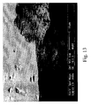
- the polishing of these substrates leads to large open porosity (pores several micron deep and wide), which cannot be excluded with polishing (see Fig. 12, Fig. 13 and Fig. 14).
- the quality of the MIC film, e.g. AIC film, should be evaluated on the substrate material between these large pores.
- the present invention provides a method for improving the MIC, especially e.g. the AIC process on microrough substrates as for instance ceramic substrates, as for instance mullite or alumina substrates.
- the quality of the polycrystalline layer resulting from the MIC, especially AIC process is at least partially determined by the microroughness of the underlying layer.
- the present invention discloses a method for the formation of a crystalline silicon layer on a face of a substrate, the face being microrough, the method comprising the steps of:
- the reduction of the microroughness of the microrough face is performed by depositing a microflattening layer on this microrough face.
- the microflattening layer is preferably a dielectric layer, for example an oxide layer, but is not limited thereto.
- the intermediate dielectric layer should lead to a substrate surface with a smaller microroughness. In that case this results in an MIC seed layer, e.g. an AIC seed layer, with much larger grains and a much lower islands density.
- a polycrystalline silicon layer on ceramic with large grain size is obtained. With large grain size is meant a grain size larger than 5 ⁇ m.
- the initial microrough substrate preferably comprises a ceramic material, glass or a glass-ceramic material.
- the substrate can be any microrough substrate. Preferably it comprises mullite, alumina or Silicon Nitride.
- any reduction of microroughness of the underlying layer or substrate results in a better performance of the MIC, e.g. AIC, process on top.
- the value ⁇ RN indicates on which substrate MIC, e.g. AIC, will give the best results.
- An additional microroughness reducing step can be applied. The same step may have a different impact on the microroughness of different substrates.
- ⁇ RN parameter only takes into account geometric features of a substrate surface, it is believed that its use for comparing ⁇ RN values is even more appropriate when comparing values on the same types of substrates, or still more appropriate when comparing values on a single substrate before and after a microflattening step. It can of course also be used to develop techniques for performing microflattening steps.
- the dielectric comprises a spin-on dielectric, e.g. spin-on oxide, a flowable dielectric, e.g. flowable oxide (which can sometimes also be a spin-on oxide), a dip-on dielectric, e.g. dip-on oxide, or a spray-on dielectric, e.g. spray-on oxide. More preferably the dielectric may comprise a spin-on glass or SiO 2 .
- the metal induced crystallisation process is preferably a Aluminum induced crystallisation process.
- the metal or Aluminum induced crystallisation process is known in the art, and typically comprises the steps of (e.g. AIC):
- the resulting seed layer can then advantageously be used for further epitaxial layer deposition, resulting in a polycrystalline layer of high quality.
- This epitaxially deposited layer can then advantageously be used for solar cell applications and manufacturing.
- the present invention also includes a substrate with a buried microrough surface, a microflattening layer on the microrrough surface, and a seed layer.
- a crystalline semiconductor layer can be provided on the seed layer.
- a solar cell can include the substrate.
- the substrates e.g. ceramic substrates
- the substrates for use with the present invention have to fulfil several other criteria regarding thermal expansion, chemical stability and optical properties.
- Alumina (microcrystalline aluminium oxide) and mullite (mixture of SiO 2 and Al 2 O 3 ) substrates have been used for the examples given below.
- the bulk of the literature on AIC deals with doing the process on glass substrates. It is however not straightforward to extend this experience to ceramic substrates. The conditions are very different.
- the ceramic substrates show a large macroroughness, ranging from 50 nm up to microns and are moreover microrough. This surface structure results from the sintering process which occurs during ceramic production.
- the alumina substrates used for the present invention had a peak to peak roughness of about 400 nm (RMS roughness ⁇ 80 nm).
- ceramic consists at least in part of a crystalline phase, in contrast to the amorphous structure of glass.
- the degree of macroroughness can be quantified by the maximum deviation from an average level line 11, as illustrated in Fig.15.
- An average level line 11 is a reference line from which profile deviations are measured.
- the least squares mean line which is a line through a profile 12 such that the sum of the squares of the deviations 10 of the profile from the average level line 11 is minimised.
- a measure for the macroroughness can be the maximum deviation from this average level line 11.
- Such average level line 11 can be determined from cross-sectional SEM or TEM pictures over a distance of minimum 1 ⁇ m and long enough to have a characteristic profile for the sample (typically maximum 15 ⁇ m).
- a surface is defined as macrorough when the maximum deviation from the average level line 11 exceeds 50 nm. If not, the surface is defined to be macroflat.
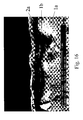
- Fig.15 the difference between macroroughness and microroughness is illustrated. Both profiles 12 illustrated are macrorough and have about the same RMS roughness. However, the top profile 12 has a larger microroughness than the bottom profile 12.
- a cross-section is shown of a sample ceramic/spin-on oxide/AIC layer.
- the ceramic substrate 1a has a macrorough and microrough surface.
- the spin-on oxide layer has a microflat but macrorough interface with the AIC seed layer 2a.
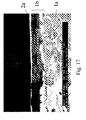
- Fig.17 shows a cross-section of a sample ceramic/spin-on oxide/AIC layer with double spin-on oxide layer.
- the ceramic substrate 1a has a macrorough and microrough surface.
- the interface between the double spin-on oxidelayer 1b and the AIC seed layer 2a is both micro- and macroflat.
- the substrates used were alumina substrates ADS996 from CoorsTek. Double layers of Aluminum and amorphous silicon were deposited one after the other, allowing the aluminium layer to get oxidized between the two depositions by a 2 min exposure to air.
- the aluminium deposition has been done in an electron-beam, high-vacuum evaporator.
- the amorphous Silicon layer was either deposited in the same evaporator, or in a parallel plate plasma-enhanced CVD system from silane decomposition.
- a typical stack was 200 nm Al and 230-250 nm Si.
- the morphology of a typical sample obtained with the procedure described above can be seen in the SEM picture in Figure 1.
- the AIC seed layer 2a as such is not clearly visible in this picture. The reason is that the layer 2a is covered by numerous 'islands' 3, the secondary crystallites formed within the top layer during the AIC process. Close observation with SEM and TEM analysis reveals that the grain size in the AIC seed layer 2a is around 1-2 ⁇ m. This grain size is substantially lower than reported results on glass. There appears to be much more nucleation taking place when the AIC is done on a ceramic substrate 1a, both in the bottom layer (leading to a small grain size) and in the top layer (leading to a high density of islands).
- An intermediate silicon oxide layer has been introduced between the substrate 1a and the AIC layers.
- Two different types of oxide have been used.
- One type is a pyrolithic oxide ('pyrox') deposited by the decomposition of silane at atmospheric pressure and 400 °C.
- the second type is a spin-on flowable oxide (FOx-23 from Dow Corning), cured at 400 °C.
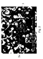
- Pyrox was densified at 950 °C and the spin-on flowable oxide at 900°C before the deposition of the AIC stack. SEM pictures of these samples are shown in Figure 2 and Figure 3, respectively.
- the density of islands 3 decreases drastically, by about a factor two for the intermediate pyrox layer (Fig.
- the appearance of the latter samples is however completely different. Because there are much less islands 3 in case of the spin-on oxide as the intermediate layer than in the other two cases, the structure of the main AIC seeding layer 2a is clearly visible, and is in fact reminiscent of what is obtained on glass substrates.
- the layer 2a consists of roughly circular large grains (> 5 ⁇ m), the growth of which is stopped by the encounter with a neighbouring grain. If the process is not allowed to proceed to full completion, or, as for these samples, the excess of Si is not sufficient, holes remain in the AIC seed layer 2a.
- This tolerance to not perfectly flat substrates is a strength of the AIC process, which is not only useful for ceramic substrates but also for glass substrates.
- the SEM picture in Figure 4 shows a not yet complete AIC seed layer 2a, it is relatively simple to achieve such a complete layer by tuning the properties of the AIC stack.
- high temperature CVD After removal of the metal layer obtained on top of the stack at the end of the MIC process, e.g. an Al layer in case of a AIC process, high temperature CVD has been used to deposit an epitaxial layer on top of the seed layer 2a, an established technique common in the microelectronics processing.
- AIC seed layers 2a have been prepared on spin-on flowable oxide 1b covered 5 ⁇ 5 cm 2 alumina samples 1a following the procedure described above. The conditions were such that the AIC layers 2a covered the complete surface. No attempt was made at removing the islands 3 from the seed layer 2a.
- Si layers 2b were deposited on these samples in a commercial single-wafer epitaxial reactor (Epsilon ASM) with trichlorosilane diluted in H2, at atmospheric pressure and at a temperature of 1130 °C. The deposition rate was 1.4 ⁇ m/min.
- In situ doping with B was done by adding diborane to the gas flow, so as to form double layers with a 0.5-3 ⁇ m thick p+ region ( ⁇ 10 19 cm-3) and a 0.5-3 ⁇ m thick p region (variable doping).
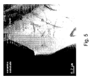
- FIG. 5 A TEM cross-section of a sample with structure alumina ceramic 1a/spin-on flowable oxide 1b/AIC seed layer 2a/epitaxial layer 2b is shown in Figure 5.
- the intermediate spin-on oxide 1b reduces the roughness but does not completely flatten the sample's surface. It does though reduce the microroughness.
- the quality of the epitaxial layer 2b appears very good.
- the seed layer 2a cannot be distinguished from the epitaxial layer 2b, no interface between the two regions being visible.
- the cross-sections show a very low defect density.
- the bent diffraction lines visible in Figure 5 do indicate that there is substantial stress in the layer. No needle-like grains, (as would be expected as a result of epitaxy on islands 3) have been observed.
- the Si layer 2b of some of the samples has been polished, a defect etch has been applied and these planar sections have been studied under an optical microscope (see Figure 6).
- the nominal grain size as determined by the grain boundary 4 counting technique is about 5 ⁇ m, while some grains reach 10 ⁇ m diameter or even larger.
- Any standard solar cell manufacturing technique can be used to produce photovoltaic cells as solar cells from the obtained structures.
- the following example was though performed to illustrate the quality of the epitaxial layer 2b.
- the mesa structure is useful for relatively fast experiments to assess the quality of the material, but has an intrinsic limitation.
- the majority carriers (holes) have to travel a large distance to reach the base contact at the periphery, over a path with low conductance, the thin p+ layer. Therefore it is normal that the series resistance is rather high.
- table 2 shows the illuminated IV parameters of these solar cells for various doping levels.
- the best efficiency so far with diffusion emitter is 5.0 %, with a Voc of 460 mV.
- the shunt resistance is not a problem, with Rsh above 1000 ohm cm 2 for all samples.
- the series resistance is as expected rather high, exceeding 3 ohm cm 2 for the best cell.
- the base doping level appears to have a minor impact on the cell parameters.
- the ceramic substrates used in this experiment are commercial mullite substrates.
- the polishing of these substrates leads to large open porosity (pores several micron deep and wide), as illustrated in Fig. 12, Fig. 13 and Fig. 14.
- the quality of the AIC film should be evaluated on the material between these large pores.
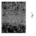
- Sample 4 non-polished mullite/AIC is illustrated in Fig. 7
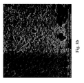
- Sample 1 polished mullite/AIC is illustrated in Fig. 8 and Fig 24 (EBSD map).
- Sample 1 is better than sample 4, i.e. it gives better results to apply AIC onto a polished substrate than to a non-polished substrate:
- Doing the MIC process on a polished ceramic substrate 1a does lead to larger grain sizes and less islands 3 than on a non-polished ceramic substrate.
- Sample 4 non-polished mullite/AIC is illustrated in Fig. 7
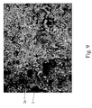
- Sample 8 non-polished mullite/sp-on ox/AIC is illustrated in Fig.9
- Sample 8 (Fig.9) is better than sample 4 (Fig.7), i.e. it gives a better result to apply AIC onto a non-polished substrate with flattening layer than onto a non-polished substrate without flattening layer:
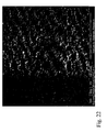
- Fig. 1 and Fig. 22 SEM: Alumina/AIC.
- Fig. 3 and Fig. 11b SEM: Alumina/spin-on oxide/AIC Samples in Fig 3 and Fig. 11b are better than samples in Fig. 1 and Fig. 22, which again indicates that it gives a better result to apply AIC onto a non-polished substrate with flattening layer than onto a non-polished substrate without flattening layer:
- micro flattening layer e.g. spin-on oxide
- Sample 1 polished mullite/AIC is illustrated in Fig. 8a and Fig 24 (EBSD map).
- Sample 5 polished mullite/spin-on oxide/AIC is illustrated in Fig. 10a and Fig. 25 (EBSD map)
- Fig. 8b is a SEM image of such a sample, where it is possible to see the holes in the Si seed layer and the islands 3 on top of the Si seed layer. Besides the holes in the seeding layer there are also holes in the substrate, as no flattening layer was applied to fill those holes.
- Fig.10b is a SEM image of such a sample. The density of holes and islands is decreased in comparison with sample 1. The big holes in the substrate are still present; the flattening layer used was not capable to completely fill these holes.
- mullite is microflat and macroflat on some areas due to polishing.
- the flattening layer reduces the number of areas still having microroughness, which results in better seed layers, with less holes and islands. But because polished mullite per se is already microflat and macroflat on many areas of the substrate, the influence of the flattening layer is less than with alumina (see below).
- Sample 5 is better than sample 1, i.e. it gives a better result to apply AIC onto a polished substrate with micro flattening layer than to apply in onto a polished substrate without micro flattening layer.
- micro flattening layer e.g. spin-on oxide
- MIC layer large grain, less islands
- micro flattening layer leads to a substantial improvement of the MIC layer (larger grains, less islands) compared to the case without micro flattening layer, and this for both polished and unpolished substrates.
- MIC e.g. AIC
- TEM pictures give also a proof for the increased grain size when using a flattening layer, e.g. spin-on oxide.
- Sample 5 polished mullite/spin-on oxide/AIC is illustrated in Fig.10a, a SEM image in Fig 10b.
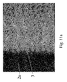
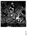
- Sample 9 alumina/FOx/poly Si is illustrated in Fig.11a, its EBSD map in Fig. 23 and a SEM image of the same area in Fig 11b.
- Fig.11b is a SEM image of such a sample, where it is possible to see the holes in the poly Si layer and the islands 3 on top of the poly Si layer.
- An EBSD pattern is related to grain orientation. At places where holes and islands are located is not always possible to determine the orientation due to partly shadowing of the EBSD patterns. For the above sample it was possible to determine the orientation on 86.1% of the surface. Corresponding EBSD measurement on alumina samples without FOx gives only orientation data on 0.3% of the surface, which shows that the surface, where there are a lot of islands, is too rough.
- a macroflat surface can for instance be achieved by twice spinning a flowable oxide over a surface.
- Fig.16 compared to Fig.17, the first one showing a cross-section of a sample ceramic 1a/spin-on oxide 1 b/AIC layer 2a, and the second one showing a cross-section of a sample ceramic 1a/spin- on oxide 1b/AIC layer 2a, with double spin-on oxide layer.
- the spin-on oxide layer 1 b/AIC layer 2a interface is both micro- and macroflat.
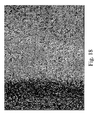
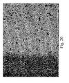
- Fig.18, resp. 20 show a top view optical microscope picture of a sample ceramic 1a/spin-on oxide 1b/AIC layer 2a after aluminium removal.
- the spin-on oxide layer 1b consists of one single layer, which in case of Fig.20, the spin-on oxide layer 1b consists of a double spin-on oxide layer. It can be seen that in case of the double spin-on oxide layer a flatter seed layer is obtained than in case of the single spin-on oxide layer.
- the AIC layer in Fig.18 has a lower quality compared to the quality of the AIC layer in Fig. 11a (both alumina/spin-on oxide/AIC), because the spin-on oxide layer is thinner (more macroroughness).
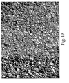
- Fig.19, resp. 21 show a top view optical microscope picture of a sample ceramic 1a/ spin-on oxide 1b/AIC layer 2a after epitaxial growth.
- the FOx layer 1b consists of one single layer, which in case of Fig.21, the spin-on oxide layer 1b consists of a double spin-on oxide layer. It can be seen that in case of the double spin-on oxide layer bigger structures are obtained than in the case of one single spin-on oxide layer, which is an indication for bigger grains, and thus better epitaxial quality.
Landscapes
- Chemical & Material Sciences (AREA)
- Engineering & Computer Science (AREA)
- Crystallography & Structural Chemistry (AREA)
- Materials Engineering (AREA)
- Metallurgy (AREA)
- Organic Chemistry (AREA)
- Physics & Mathematics (AREA)
- Thermal Sciences (AREA)
- Crystals, And After-Treatments Of Crystals (AREA)
- Liquid Deposition Of Substances Of Which Semiconductor Devices Are Composed (AREA)
- Physical Deposition Of Substances That Are Components Of Semiconductor Devices (AREA)
Applications Claiming Priority (2)
| Application Number | Priority Date | Filing Date | Title |
|---|---|---|---|
| US577556 | 1990-09-05 | ||
| US57755604P | 2004-06-07 | 2004-06-07 |
Publications (2)
| Publication Number | Publication Date |
|---|---|
| EP1605499A2 true EP1605499A2 (fr) | 2005-12-14 |
| EP1605499A3 EP1605499A3 (fr) | 2009-12-02 |
Family
ID=34943295
Family Applications (1)
| Application Number | Title | Priority Date | Filing Date |
|---|---|---|---|
| EP05447132A Ceased EP1605499A3 (fr) | 2004-06-07 | 2005-06-07 | Procédé de fabrication d'une couche de silicium cristallin |
Country Status (2)
| Country | Link |
|---|---|
| US (1) | US7662702B2 (fr) |
| EP (1) | EP1605499A3 (fr) |
Cited By (3)
| Publication number | Priority date | Publication date | Assignee | Title |
|---|---|---|---|---|
| WO2009150159A1 (fr) * | 2008-06-09 | 2009-12-17 | Dritte Patentportfolio Beteiligungsgesellschaft Mbh & Co. Kg. | Procédé de production de couches polycristallines |
| US7719949B2 (en) | 2006-01-27 | 2010-05-18 | Funai Electric Co., Ltd. | Optical head |
| WO2016201526A1 (fr) * | 2015-06-19 | 2016-12-22 | Chee Yee Kwok | Film de silicium et procédé pour former un film de silicium |
Families Citing this family (7)
| Publication number | Priority date | Publication date | Assignee | Title |
|---|---|---|---|---|
| US7608530B2 (en) * | 2007-03-01 | 2009-10-27 | Hewlett-Packard Development Company, L.P. | Hetero-crystalline structure and method of making same |
| US8183566B2 (en) * | 2007-03-01 | 2012-05-22 | Hewlett-Packard Development Company, L.P. | Hetero-crystalline semiconductor device and method of making same |
| US8273983B2 (en) * | 2007-12-21 | 2012-09-25 | Hewlett-Packard Development Company, L.P. | Photonic device and method of making same using nanowires |
| US20090188557A1 (en) * | 2008-01-30 | 2009-07-30 | Shih-Yuan Wang | Photonic Device And Method Of Making Same Using Nanowire Bramble Layer |
| DE102009031357A1 (de) * | 2009-07-01 | 2011-01-05 | Fraunhofer-Gesellschaft zur Förderung der angewandten Forschung e.V. | Kristalline Siliciumschicht auf einem Substrat, Verfahren zu deren Herstellung und Verwendung |
| EP2474023A1 (fr) | 2009-09-02 | 2012-07-11 | Imec | Procédé de fabrication d'une couche de silicium cristallin |
| CN101853784B (zh) * | 2010-05-17 | 2012-07-04 | 广东中显科技有限公司 | 一种横向诱导晶化低温多晶硅薄膜的方法 |
Family Cites Families (12)
| Publication number | Priority date | Publication date | Assignee | Title |
|---|---|---|---|---|
| US3961997A (en) * | 1975-05-12 | 1976-06-08 | The United States Of America As Represented By The Administrator Of The National Aeronautics And Space Administration | Fabrication of polycrystalline solar cells on low-cost substrates |
| US4400715A (en) * | 1980-11-19 | 1983-08-23 | International Business Machines Corporation | Thin film semiconductor device and method for manufacture |
| US4818337A (en) * | 1986-04-11 | 1989-04-04 | University Of Delaware | Thin active-layer solar cell with multiple internal reflections |
| JP2804839B2 (ja) * | 1990-10-17 | 1998-09-30 | 三菱電機株式会社 | 半導体装置の製造方法 |
| JP3417665B2 (ja) * | 1994-07-07 | 2003-06-16 | 株式会社東芝 | 半導体装置の製造方法 |
| US5844351A (en) * | 1995-08-24 | 1998-12-01 | Fed Corporation | Field emitter device, and veil process for THR fabrication thereof |
| DE19647635A1 (de) * | 1996-11-18 | 1998-05-20 | Wacker Siltronic Halbleitermat | Verfahren und Vorrichtung zum Entfernen einer Halbleiterscheibe von einer ebenen Unterlage |
| US6241817B1 (en) * | 1997-05-24 | 2001-06-05 | Jin Jang | Method for crystallizing amorphous layer |
| US6099662A (en) * | 1999-02-11 | 2000-08-08 | Taiwan Semiconductor Manufacturing Company | Process for cleaning a semiconductor substrate after chemical-mechanical polishing |
| US6562668B2 (en) * | 2000-08-12 | 2003-05-13 | Jin Jang | Method of fabricating thin film transistor using buffer layer and the thin film transistor |
| JP2002203942A (ja) * | 2000-12-28 | 2002-07-19 | Fuji Electric Co Ltd | パワー半導体モジュール |
| AU2002951838A0 (en) * | 2002-10-08 | 2002-10-24 | Unisearch Limited | Method of preparation for polycrystalline semiconductor films |
-
2005
- 2005-06-07 EP EP05447132A patent/EP1605499A3/fr not_active Ceased
- 2005-06-07 US US11/146,564 patent/US7662702B2/en not_active Expired - Fee Related
Non-Patent Citations (6)
| Title |
|---|
| E PIHAN; A. SLAOUI; M. RUSU: "Formation of polycrystalline silicon on foreign substrates by combination of CVD and Aluminium-Induced crystallisation techniques", CONFERENCE ''PV IN EUROPE, 2002 |
| JEF POORTMANS ET AL: "Crystalline Silicon Thin Film Solar Cells on Foreign Substrates by High Temperature Deposition and Recrystallization", 1 January 2006, THIN FILM SOLAR CELLS: FABRICATION, CHARACTERIZATION AND APPLICATIONS, JOHN WILEY & SONS, LTD, PAGE(S) 39 - 96, ISBN: 978-0-470-09126-5, XP009114689 * |
| N.-P. HARDER ET AL., PROCEEDINGS 28TH IEEE PVSC, 2000 |
| S. BREHME ET AL., IEEE TRANS. EL. DEV., vol. 46, 1999, pages 2062 |
| S. GALL ET AL., PROCEEDINGS PV IN EUROPE, 2002, pages 87 |
| U. RAU K. TARETTO; J. H. WERNER, J. APPL PHYS., vol. 93, 2003, pages 5447 |
Cited By (3)
| Publication number | Priority date | Publication date | Assignee | Title |
|---|---|---|---|---|
| US7719949B2 (en) | 2006-01-27 | 2010-05-18 | Funai Electric Co., Ltd. | Optical head |
| WO2009150159A1 (fr) * | 2008-06-09 | 2009-12-17 | Dritte Patentportfolio Beteiligungsgesellschaft Mbh & Co. Kg. | Procédé de production de couches polycristallines |
| WO2016201526A1 (fr) * | 2015-06-19 | 2016-12-22 | Chee Yee Kwok | Film de silicium et procédé pour former un film de silicium |
Also Published As
| Publication number | Publication date |
|---|---|
| US7662702B2 (en) | 2010-02-16 |
| EP1605499A3 (fr) | 2009-12-02 |
| US20060030132A1 (en) | 2006-02-09 |
Similar Documents
| Publication | Publication Date | Title |
|---|---|---|
| US7709360B2 (en) | Method for manufacturing a crystalline silicon layer | |
| US20120248455A1 (en) | Process for manufacturing a crystalline silicon layer | |
| US6258637B1 (en) | Method for thin film deposition on single-crystal semiconductor substrates | |
| US20110212600A1 (en) | Method for forming channel layer with high ge content on substrate | |
| Gordon et al. | Thin-film polycrystalline silicon solar cells on ceramic substrates by aluminium-induced crystallization | |
| JP2004523903A (ja) | 薄膜及びトリシランを用いる薄膜の形成方法 | |
| EP2047501A1 (fr) | Dépôt de nitrures du groupe iii sur ge | |
| Van Nieuwenhuysen et al. | Progress in epitaxial deposition on low-cost substrates for thin-film crystalline silicon solar cells at IMEC | |
| Van Gestel et al. | Intragrain defects in polycrystalline silicon layers grown by aluminum-induced crystallization and epitaxy for thin-film solar cells | |
| US8502191B2 (en) | Semiconductor device, manufacturing method therefor, and solar cell | |
| US11634834B2 (en) | Diamond on nanopatterned substrate | |
| US7662702B2 (en) | Method for manufacturing a crystalline silicon layer | |
| TW201838194A (zh) | 垂直氮化鎵蕭特基二極體 | |
| TWI613832B (zh) | 在矽基質上形成鍺層之方法及包含鍺層之光伏裝置 | |
| US8329532B2 (en) | Process for the simultaneous deposition of crystalline and amorphous layers with doping | |
| TW200524146A (en) | Semiconductor substrate and method for production thereof | |
| EP0557890A2 (fr) | Procédé de croissance d'une structure épitaxiale métal-isolant-métal-semi-conducteur | |
| Slaoui et al. | Thin-film silicon solar cells on mullite substrates | |
| WO2023047864A1 (fr) | Substrat semi-conducteur au nitrure et son procédé de production | |
| CN119278499A (zh) | 半导体晶圆的制造方法及半导体晶圆 | |
| Pihan et al. | Crystallographic analysis of polysilicon films formed on foreign substrates by aluminium induced crystallisation and epitaxy | |
| JP2022067962A (ja) | Soiウェーハの製造方法及びsoiウェーハ | |
| US20230268222A1 (en) | Method for manufacturing soi wafer and soi wafer | |
| CN114267628A (zh) | 超薄绝缘体上硅(soi)衬底基片及其制备方法 | |
| Gall et al. | Large-grained polycrystalline silicon thin-film solar cells using AIC seed layers |
Legal Events
| Date | Code | Title | Description |
|---|---|---|---|
| PUAI | Public reference made under article 153(3) epc to a published international application that has entered the european phase |
Free format text: ORIGINAL CODE: 0009012 |
|
| AK | Designated contracting states |
Kind code of ref document: A2 Designated state(s): AT BE BG CH CY CZ DE DK EE ES FI FR GB GR HU IE IS IT LI LT LU MC NL PL PT RO SE SI SK TR |
|
| AX | Request for extension of the european patent |
Extension state: AL BA HR LV MK YU |
|
| RAP1 | Party data changed (applicant data changed or rights of an application transferred) |
Owner name: IMEC |
|
| PUAL | Search report despatched |
Free format text: ORIGINAL CODE: 0009013 |
|
| AK | Designated contracting states |
Kind code of ref document: A3 Designated state(s): AT BE BG CH CY CZ DE DK EE ES FI FR GB GR HU IE IS IT LI LT LU MC NL PL PT RO SE SI SK TR |
|
| AX | Request for extension of the european patent |
Extension state: AL BA HR LV MK YU |
|
| 17P | Request for examination filed |
Effective date: 20100308 |
|
| 17Q | First examination report despatched |
Effective date: 20100429 |
|
| AKX | Designation fees paid |
Designated state(s): AT BE BG CH CY CZ DE DK EE ES FI FR GB GR HU IE IS IT LI LT LU MC NL PL PT RO SE SI SK TR |
|
| STAA | Information on the status of an ep patent application or granted ep patent |
Free format text: STATUS: THE APPLICATION HAS BEEN REFUSED |
|
| 18R | Application refused |
Effective date: 20120320 |