EP1607940A2 - Compositions améliorées d'alliages d'un cible à pulvérisation - Google Patents
Compositions améliorées d'alliages d'un cible à pulvérisation Download PDFInfo
- Publication number
- EP1607940A2 EP1607940A2 EP05252880A EP05252880A EP1607940A2 EP 1607940 A2 EP1607940 A2 EP 1607940A2 EP 05252880 A EP05252880 A EP 05252880A EP 05252880 A EP05252880 A EP 05252880A EP 1607940 A2 EP1607940 A2 EP 1607940A2
- Authority
- EP
- European Patent Office
- Prior art keywords
- atomic percent
- sputter target
- much
- group
- magnetic recording
- Prior art date
- Legal status (The legal status is an assumption and is not a legal conclusion. Google has not performed a legal analysis and makes no representation as to the accuracy of the status listed.)
- Withdrawn
Links
- 229910045601 alloy Inorganic materials 0.000 title claims description 27
- 239000000956 alloy Substances 0.000 title claims description 27
- 239000000203 mixture Substances 0.000 title description 9
- 230000005291 magnetic effect Effects 0.000 claims abstract description 50
- 239000010409 thin film Substances 0.000 claims abstract description 42
- 229910052750 molybdenum Inorganic materials 0.000 claims abstract description 25
- 229910052721 tungsten Inorganic materials 0.000 claims abstract description 24
- 229910052772 Samarium Inorganic materials 0.000 claims abstract description 14
- 229910052691 Erbium Inorganic materials 0.000 claims abstract description 13
- 229910052693 Europium Inorganic materials 0.000 claims abstract description 13
- 229910052688 Gadolinium Inorganic materials 0.000 claims abstract description 13
- 229910052689 Holmium Inorganic materials 0.000 claims abstract description 13
- 229910052765 Lutetium Inorganic materials 0.000 claims abstract description 13
- 229910052779 Neodymium Inorganic materials 0.000 claims abstract description 13
- 229910052777 Praseodymium Inorganic materials 0.000 claims abstract description 13
- 229910052769 Ytterbium Inorganic materials 0.000 claims abstract description 13
- 229910052738 indium Inorganic materials 0.000 claims abstract description 13
- 229910052746 lanthanum Inorganic materials 0.000 claims abstract description 13
- 229910052716 thallium Inorganic materials 0.000 claims abstract description 13
- 229910052748 manganese Inorganic materials 0.000 claims abstract description 9
- 229910052727 yttrium Inorganic materials 0.000 claims abstract description 9
- 229910052741 iridium Inorganic materials 0.000 claims abstract description 8
- 229910052715 tantalum Inorganic materials 0.000 claims abstract description 8
- 229910052735 hafnium Inorganic materials 0.000 claims abstract description 6
- 229910052758 niobium Inorganic materials 0.000 claims abstract description 6
- 229910052763 palladium Inorganic materials 0.000 claims abstract description 6
- 229910052703 rhodium Inorganic materials 0.000 claims abstract description 6
- 229910052707 ruthenium Inorganic materials 0.000 claims abstract description 6
- 229910052719 titanium Inorganic materials 0.000 claims abstract description 6
- 229910052720 vanadium Inorganic materials 0.000 claims abstract description 6
- 229910052726 zirconium Inorganic materials 0.000 claims abstract description 6
- 239000000758 substrate Substances 0.000 claims description 16
- 238000000034 method Methods 0.000 claims description 14
- 238000004544 sputter deposition Methods 0.000 claims description 11
- 238000004519 manufacturing process Methods 0.000 claims description 7
- 239000010410 layer Substances 0.000 description 31
- 239000011651 chromium Substances 0.000 description 27
- 239000010949 copper Substances 0.000 description 14
- 229910052796 boron Inorganic materials 0.000 description 12
- ZOXJGFHDIHLPTG-UHFFFAOYSA-N Boron Chemical compound [B] ZOXJGFHDIHLPTG-UHFFFAOYSA-N 0.000 description 11
- 239000000654 additive Substances 0.000 description 9
- 229910052804 chromium Inorganic materials 0.000 description 9
- 150000001875 compounds Chemical class 0.000 description 9
- 230000005415 magnetization Effects 0.000 description 9
- 229910052697 platinum Inorganic materials 0.000 description 9
- VYZAMTAEIAYCRO-UHFFFAOYSA-N Chromium Chemical compound [Cr] VYZAMTAEIAYCRO-UHFFFAOYSA-N 0.000 description 8
- 230000000996 additive effect Effects 0.000 description 8
- 239000000463 material Substances 0.000 description 8
- 238000000926 separation method Methods 0.000 description 8
- 229910017052 cobalt Inorganic materials 0.000 description 7
- 239000010941 cobalt Substances 0.000 description 7
- GUTLYIVDDKVIGB-UHFFFAOYSA-N cobalt atom Chemical compound [Co] GUTLYIVDDKVIGB-UHFFFAOYSA-N 0.000 description 7
- 230000008878 coupling Effects 0.000 description 6
- 238000010168 coupling process Methods 0.000 description 6
- 238000005859 coupling reaction Methods 0.000 description 6
- 239000011159 matrix material Substances 0.000 description 6
- 238000005204 segregation Methods 0.000 description 6
- 238000013500 data storage Methods 0.000 description 5
- 238000010587 phase diagram Methods 0.000 description 5
- 230000007704 transition Effects 0.000 description 5
- RYGMFSIKBFXOCR-UHFFFAOYSA-N Copper Chemical compound [Cu] RYGMFSIKBFXOCR-UHFFFAOYSA-N 0.000 description 4
- 229910052802 copper Inorganic materials 0.000 description 4
- 230000002349 favourable effect Effects 0.000 description 4
- 229910017885 Cu—Pt Inorganic materials 0.000 description 3
- 238000007792 addition Methods 0.000 description 3
- 239000010408 film Substances 0.000 description 3
- 239000011229 interlayer Substances 0.000 description 3
- 239000000314 lubricant Substances 0.000 description 3
- 230000006911 nucleation Effects 0.000 description 3
- 238000010899 nucleation Methods 0.000 description 3
- 230000008569 process Effects 0.000 description 3
- 150000002910 rare earth metals Chemical group 0.000 description 3
- 230000001603 reducing effect Effects 0.000 description 3
- 230000009467 reduction Effects 0.000 description 3
- 229920006395 saturated elastomer Polymers 0.000 description 3
- 239000013077 target material Substances 0.000 description 3
- 230000000930 thermomechanical effect Effects 0.000 description 3
- 239000000470 constituent Substances 0.000 description 2
- 238000005530 etching Methods 0.000 description 2
- 230000005496 eutectics Effects 0.000 description 2
- 230000005294 ferromagnetic effect Effects 0.000 description 2
- 238000005457 optimization Methods 0.000 description 2
- 238000001556 precipitation Methods 0.000 description 2
- 238000012545 processing Methods 0.000 description 2
- 239000006104 solid solution Substances 0.000 description 2
- 229910020637 Co-Cu Inorganic materials 0.000 description 1
- 229910020707 Co—Pt Inorganic materials 0.000 description 1
- 229910016551 CuPt Inorganic materials 0.000 description 1
- 229910017816 Cu—Co Inorganic materials 0.000 description 1
- 229910017813 Cu—Cr Inorganic materials 0.000 description 1
- 238000013459 approach Methods 0.000 description 1
- XKRFYHLGVUSROY-UHFFFAOYSA-N argon Substances [Ar] XKRFYHLGVUSROY-UHFFFAOYSA-N 0.000 description 1
- 229910052786 argon Inorganic materials 0.000 description 1
- -1 argon ion Chemical class 0.000 description 1
- 230000009286 beneficial effect Effects 0.000 description 1
- 230000015572 biosynthetic process Effects 0.000 description 1
- 230000000295 complement effect Effects 0.000 description 1
- 238000005260 corrosion Methods 0.000 description 1
- 230000007797 corrosion Effects 0.000 description 1
- 238000005336 cracking Methods 0.000 description 1
- 230000003247 decreasing effect Effects 0.000 description 1
- 210000001787 dendrite Anatomy 0.000 description 1
- 238000000151 deposition Methods 0.000 description 1
- 230000008021 deposition Effects 0.000 description 1
- 238000009826 distribution Methods 0.000 description 1
- 230000000694 effects Effects 0.000 description 1
- 230000003628 erosive effect Effects 0.000 description 1
- 150000002500 ions Chemical class 0.000 description 1
- 229910001004 magnetic alloy Inorganic materials 0.000 description 1
- 239000000696 magnetic material Substances 0.000 description 1
- 238000001755 magnetron sputter deposition Methods 0.000 description 1
- 238000005259 measurement Methods 0.000 description 1
- 238000012986 modification Methods 0.000 description 1
- 230000004048 modification Effects 0.000 description 1
- 230000003647 oxidation Effects 0.000 description 1
- 238000007254 oxidation reaction Methods 0.000 description 1
- 230000001590 oxidative effect Effects 0.000 description 1
- 229910002059 quaternary alloy Inorganic materials 0.000 description 1
- 238000009877 rendering Methods 0.000 description 1
- 238000001878 scanning electron micrograph Methods 0.000 description 1
- 239000004065 semiconductor Substances 0.000 description 1
- 239000007787 solid Substances 0.000 description 1
- 238000005477 sputtering target Methods 0.000 description 1
Images


Classifications
-
- G—PHYSICS
- G11—INFORMATION STORAGE
- G11B—INFORMATION STORAGE BASED ON RELATIVE MOVEMENT BETWEEN RECORD CARRIER AND TRANSDUCER
- G11B5/00—Recording by magnetisation or demagnetisation of a record carrier; Reproducing by magnetic means; Record carriers therefor
- G11B5/84—Processes or apparatus specially adapted for manufacturing record carriers
- G11B5/851—Coating a support with a magnetic layer by sputtering
-
- C—CHEMISTRY; METALLURGY
- C22—METALLURGY; FERROUS OR NON-FERROUS ALLOYS; TREATMENT OF ALLOYS OR NON-FERROUS METALS
- C22C—ALLOYS
- C22C19/00—Alloys based on nickel or cobalt
- C22C19/07—Alloys based on nickel or cobalt based on cobalt
-
- C—CHEMISTRY; METALLURGY
- C23—COATING METALLIC MATERIAL; COATING MATERIAL WITH METALLIC MATERIAL; CHEMICAL SURFACE TREATMENT; DIFFUSION TREATMENT OF METALLIC MATERIAL; COATING BY VACUUM EVAPORATION, BY SPUTTERING, BY ION IMPLANTATION OR BY CHEMICAL VAPOUR DEPOSITION, IN GENERAL; INHIBITING CORROSION OF METALLIC MATERIAL OR INCRUSTATION IN GENERAL
- C23C—COATING METALLIC MATERIAL; COATING MATERIAL WITH METALLIC MATERIAL; SURFACE TREATMENT OF METALLIC MATERIAL BY DIFFUSION INTO THE SURFACE, BY CHEMICAL CONVERSION OR SUBSTITUTION; COATING BY VACUUM EVAPORATION, BY SPUTTERING, BY ION IMPLANTATION OR BY CHEMICAL VAPOUR DEPOSITION, IN GENERAL
- C23C14/00—Coating by vacuum evaporation, by sputtering or by ion implantation of the coating forming material
- C23C14/22—Coating by vacuum evaporation, by sputtering or by ion implantation of the coating forming material characterised by the process of coating
- C23C14/34—Sputtering
- C23C14/3407—Cathode assembly for sputtering apparatus, e.g. Target
- C23C14/3414—Metallurgical or chemical aspects of target preparation, e.g. casting, powder metallurgy
-
- C—CHEMISTRY; METALLURGY
- C23—COATING METALLIC MATERIAL; COATING MATERIAL WITH METALLIC MATERIAL; CHEMICAL SURFACE TREATMENT; DIFFUSION TREATMENT OF METALLIC MATERIAL; COATING BY VACUUM EVAPORATION, BY SPUTTERING, BY ION IMPLANTATION OR BY CHEMICAL VAPOUR DEPOSITION, IN GENERAL; INHIBITING CORROSION OF METALLIC MATERIAL OR INCRUSTATION IN GENERAL
- C23C—COATING METALLIC MATERIAL; COATING MATERIAL WITH METALLIC MATERIAL; SURFACE TREATMENT OF METALLIC MATERIAL BY DIFFUSION INTO THE SURFACE, BY CHEMICAL CONVERSION OR SUBSTITUTION; COATING BY VACUUM EVAPORATION, BY SPUTTERING, BY ION IMPLANTATION OR BY CHEMICAL VAPOUR DEPOSITION, IN GENERAL
- C23C28/00—Coating for obtaining at least two superposed coatings either by methods not provided for in a single one of groups C23C2/00 - C23C26/00 or by combinations of methods provided for in subclasses C23C and C25C or C25D
- C23C28/02—Coating for obtaining at least two superposed coatings either by methods not provided for in a single one of groups C23C2/00 - C23C26/00 or by combinations of methods provided for in subclasses C23C and C25C or C25D only coatings only including layers of metallic material
- C23C28/021—Coating for obtaining at least two superposed coatings either by methods not provided for in a single one of groups C23C2/00 - C23C26/00 or by combinations of methods provided for in subclasses C23C and C25C or C25D only coatings only including layers of metallic material including at least one metal alloy layer
-
- G—PHYSICS
- G11—INFORMATION STORAGE
- G11B—INFORMATION STORAGE BASED ON RELATIVE MOVEMENT BETWEEN RECORD CARRIER AND TRANSDUCER
- G11B5/00—Recording by magnetisation or demagnetisation of a record carrier; Reproducing by magnetic means; Record carriers therefor
- G11B5/62—Record carriers characterised by the selection of the material
- G11B5/64—Record carriers characterised by the selection of the material comprising only the magnetic material without bonding agent
- G11B5/65—Record carriers characterised by the selection of the material comprising only the magnetic material without bonding agent characterised by its composition
- G11B5/657—Record carriers characterised by the selection of the material comprising only the magnetic material without bonding agent characterised by its composition containing inorganic, non-oxide compound of Si, N, P, B, H or C, e.g. in metal alloy or compound
-
- H—ELECTRICITY
- H01—ELECTRIC ELEMENTS
- H01J—ELECTRIC DISCHARGE TUBES OR DISCHARGE LAMPS
- H01J37/00—Discharge tubes with provision for introducing objects or material to be exposed to the discharge, e.g. for the purpose of examination or processing thereof
- H01J37/32—Gas-filled discharge tubes
- H01J37/34—Gas-filled discharge tubes operating with cathodic sputtering
- H01J37/3411—Constructional aspects of the reactor
- H01J37/3414—Targets
- H01J37/3426—Material
- H01J37/3429—Plural materials
Definitions
- the present invention relates to sputter targets and, more particularly, relates to magnetic data-storing thin films sputtered from sputter targets which are comprised of alloy compositions with improved metallurgical characteristics.
- the process of DC magnetron sputtering is widely used in a variety of fields to provide thin film material deposition of a precisely controlled thickness and within narrow atomic fraction tolerances on a substrate, for example to coat semiconductors and/or to form films on surfaces of magnetic recording media.
- a racetrack-shaped magnetic field is applied to the sputter target by placing magnets on the backside surface of the target. Electrons are trapped near the sputtering target, improving argon ion production and increasing the sputtering rate. Ions within this plasma collide with a surface of the sputter target causing the sputter target to emit atoms from the sputter target surface.
- the voltage difference between the cathodic sputter target and an anodic substrate that is to be coated causes the emitted atoms to form the desired film on the surface of the substrate.
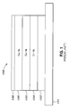
- a typical thin film stack for conventional magnetic recording media includes non-magnetic substrate base 101, seed layer 102, at least one non-magnetic, chromium-based underlayer 104, at least one slightly magnetic, cobalt-based interlayer 105, at least one magnetic data-storing layer 106, and lubricant layer 108.
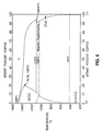
- FIG 2 illustrates a typical hysteresis loop of a data-storing thin film layer, obtained by the Vibrating Sample Magnetometer ("VSM") technique.
- VSM Vibrating Sample Magnetometer
- a VSM quasi-statically drives a magnet around its hysteresis loop using an applied field from an electromagnet. The sample is vibrated in this field, and the measurement system detects the applied field (H) and the sample's magnetization (M) in the applied field.
- Figure 2 depicts the variation of material magnetization (M) in the direction of the applied field (H).
- Zero field remnant magnetization (M r ) (or "remanence") is a measure of the remaining magnetization when the driving field is dropped to zero
- coercivity (H c ) is a measure of the reverse field needed to drive the magnetization to zero after being saturated.
- So read back signal
- the predominant materials presently used for conventional magnetic recording media are ferromagnetic, Co-Cr-Pt-B-based alloys, arranged as an array of nanoscale grains where each grain is typically 10 nm or less.
- the intergranular gap at those grain boundaries is generally very narrow, and the intergranular gap is often not sufficient to prevent magnetostatic and intergranular exchange.
- compositional segregation at grain boundaries there are three approaches to thin film noise reduction: compositional segregation at grain boundaries, multilayer application, and physical grain separation. Briefly, by applying magnetic multilayers in a stack of ferromagnetic films separated by nonmagnetic thin layers, or by sputtering a thin film at low temperatures and high pressures to generate a "voided grain structure, the noise in magnetic media can be decreased, and data storage capabilities increased.
- the sputtering parameters are very critical in tailoring the physical separation of media grains. Further study of microscopic properties, such as grain size, grain coupling, and grain crystallographic orientation is required to improve upon these techniques to improve the noise performance (N) of the thin films. Furthermore, to produce more optimal magnetic recording media, an optimization of both the macro-magnetics and micro-magnetics is warranted.
- alloys such as boron-containing alloys with improved compositional segregation, which can be used in sputter targets and sputtered into thin films with an enhanced composition.
- Preferred embodiments of the present invention solve the foregoing problems by providing a sputter target for sputtering a magnetic, data-storing thin film layer, where the sputter target is comprised of an alloy composition which effectuates the precipitation of a secondary grain boundary.
- the present invention is a sputter target, where the sputter target is comprised of Co, greater than 0 and as much as 24 atomic percent Cr, greater than 0 and as much as 20 atomic percent Pt, greater than 0 and as much as 20 atomic percent B, and greater than 0 and as much as 10 atomic percent X 1 , where X 1 is an element selected from the group consisting of Ag, Ce, Cu, Dy, Er, Eu, Gd, Ho, In, La, Lu, Mo, Nd, Pr, Sm, Tl, W, and Yb.
- the sputter target according to the present invention includes elements selected from transition, refractory and rare-earth groups. These elements are selected on their solid-state immiscibility in Co and/or Cr, and their tendency to combine with Pt to form a stoichiometrically favorable compound formula, in which the compound includes a low fraction of Pt atom and a predominant fraction of the additive element. This condition is critical for maintaining sufficient Pt atom fraction in the Co matrix in order not to sacrifice coercivity. By adding elements, which are insoluble in either cobalt or chromium, the added elements will be rejected from the Co-Pt phase, and will be forced to the grain boundaries, increasing grain separation and, consequently, improving the signal-to-noise ratio.
- the sputter target is further comprised of X 2 , wherein X 2 is selected from the group consisting of W, Y, Mn, and Mo. Moreover, the sputter target is further comprised of 0 to 7 atomic percent X 3 , wherein X 3 is an element selected from the group consisting of Ti, V, Zr, Nb, Ru, Rh, Pd, Hf, Ta, and Ir.
- the alloys forming the sputter target according to the present invention include compounds, which nucleate and grow at media grain boundaries, providing another type of physical separation of grains.
- Other additive elements with low diffusivity, such as W and Mo, are expected to provide new nucleation sites, which would allow further grain refinement and promote more Cr segregation to grain boundaries.
- the thin film sputtered by the sputter target has a coercivity value between 1000 Oersted and 4000 Oersted.
- the reverse field needed to drive the magnetization to zero after being saturated can be adjusted to fall within a user's desired parameters. Accordingly the signal-to-noise (S 0 /N) ratio will increase, and the overall magnetic properties of thin films intended at high-density magnetic recording will improve.
- the thin film layer sputtered from the sputter target has a gain of 0.5 dB to in excess of 1.5 dB in the signal-to-noise ratio over a corresponding quaternary CoCrPtB alloy, where a corresponding quaternary CoCrPtB alloy is defined as an alloy with the same atomic percentage for each of Co, Cr, Pt, and B as the Co-Cr-Pt-B- X 1 alloy, without the addition of any X 1 .
- the present invention is a magnetic recording medium including a substrate and a data-storing thin film layer formed over the substrate.
- the data-storing thin film layer is comprised of Co, greater than 0 and as much as 24 atomic percent Cr, greater than 0 and as much as 20 atomic percent Pt, greater than 0 and as much as 20 atomic percent B, and greater than 0 and as much as 10 atomic percent X 1 , wherein X 1 is an element selected from the group consisting of Ag, Ce, Cu, Dy, Er, Eu, Gd, Ho, In, La, Lu, Mo, Nd, Pr, Sm, Tl, W, and Yb.
- the present invention is a method for manufacturing a magnetic recording medium.
- the method includes the step of sputtering at least a first data-storing thin film layer over a substrate from a sputter target, where the sputter target is comprised of Co, greater than 0 and as much as 24 atomic percent Cr, greater than 0 and as much as 20 atomic percent Pt, greater than 0 and as much as 20 atomic percent B, and greater than 0 and as much as 10 atomic percent X 1 , where X 1 is an element selected from the group consisting of Ag, Ce, Cu, Dy, Er, Eu, Gd, Ho, In, La, Lu, Mo, Nd, Pr, Sm, Tl, W, and Yb.
- Embodiments of the present invention allow for increased data storage of a magnetic recording medium by adding selected fifth and/or sixth constituents to a base CoCrPtB, in order to achieve an optimal composition for the sputter target material.
- Figure 3 depicts a magnetic recording medium in which the data-storing thin film layer has been sputtered by a sputter target comprised of the enhanced composition according to one embodiment of the present invention.
- the magnetic recording medium includes a data-storing thin film layer comprised of Co, greater than 0 and as much as 24 atomic percent Cr, greater than 0 and as much as 20 atomic percent Pt, greater than 0 and as much as 20 atomic percent B, and greater than 0 and as much as 10 atomic percent X 1 , where X 1 is an element selected from the group consisting of Ag, Ce, Cu, Dy, Er, Eu, Gd, Ho, In, La, Lu, Mo, Nd, Pr, Sm, Tl, W, and Yb.
- magnetic recording medium 300 includes non-magnetic substrate base 101, seed layer 102, at least one non-magnetic, Cr-based underlayer 104, at least one slightly magnetic, Co-based interlayer 106, data-storing thin film layer 306, and lubricant layer 108.
- data-storing thin film layer on magnetic recording medium 300 is comprised of Co, greater than 0 and as much as 24 atomic percent Cr, greater than 0 and as much as 20 atomic percent Pt, greater than 0 and as much as 20 atomic percent B, and greater than 0 and as much as 10 atomic percent X 1 , where X 1 is an element selected from the group consisting of Ag, Ce, Cu, Dy, Er, Eu, Gd, Ho, In, La, Lu, Mo, Nd, Pr, Sm, Tl, W, and Yb.
- magnetic recording medium 300 omits seed layer 102, underlayer 104, interlayer 105, and/or lubricant layer 108.
- Magnetic recording medium 300 is manufactured by sputtering data-storing thin film layer 306 over a substrate 101 from a sputter target, where the sputter target is also comprised of Co, greater than 0 and as much as 24 atomic percent Cr, greater than 0 and as much as 20 atomic percent Pt, greater than 0 and as much as 20 atomic percent B, and greater than 0 and as much as 10 atomic percent X 1 , where X 1 is an element selected from the group consisting of Ag, Ce, Cu, Dy, Er, Eu, Gd, Ho, In, La, Lu, Mo, Nd, Pr, Sm, Tl, W, and Yb.
- the process of sputtering is well known in material science.
- the sputter target according to the present invention includes elements selected from transition, refractory and rare earth groups. These elements were selected on their solid-state immiscibility in Co and/or Cr, and their tendency to combine with Pt to form a stoichiometrically favorable compound formula, as discussed more fully below.
- the sputter target and corresponding data-storing thin film layer are further comprised of X 2 , wherein X 2 is selected from the group consisting of W, Y, Mn, and Mo. Moreover, the sputter target and corresponding data-storing thin film layer are further comprised of 0 to 7 atomic percent X 3 , wherein X 3 is an element selected from the group consisting of Ti, V, Zr, Nb, Ru, Rh, Pd, Hf, Ta, and Ir. In an additional alternate arrangement, elements X 2 and/or X 3 are omitted.
- the alloys forming the sputter target according to the present invention include compounds, which nucleate and grow at media grain boundaries, providing another type of physical separation of grains. Additive elements W and Mo further provide new nucleation sites which allow grain refinement and which promote more Cr segregation to grain boundaries.
- the magnetic data-storing thin film layer sputtered from the sputter target are tailored to have a coercivity value from 1000 Oersted to in excess of 4000 Oersted.
- the reverse field needed to drive the magnetization to zero after being saturated can be adjusted to fall within a user's desired parameters. Accordingly the signal-to-noise ratio will increase, and the overall magnetic properties of thin films intended at high-density magnetic recording will improve.
- Microscopic properties such as grain size, grain coupling, and grain crystallographic orientation, determine the noise performance (N) of thin films, and an optimization of the macro-magnetics and micro-magnetics is necessary to produce the optimum disk.
- the first element used in the sputter target according to one aspect of the present invention is cobalt.
- Cobalt a key element for most data storage applications, has a low coercivity, and requires the addition of large diameter transition elements such as Pt, Ta, Ir and Sm to form alloys with coercivity values from 1000 Oersted to in excess of 4000 Oersted.
- Chromium a second crucial element for data storage applications, serves two critical purposes within the alloy. First, chromium reduces the corrosion potential in the alloy by oxidizing and passivating the surface of the alloy from further oxidation. Second, the presence of chromium in the magnetic alloy allows for precipitation of other crystalline phases of other elements, such as boron, at grain boundaries or within grains, aiding in noise reduction.
- boron As discussed above, a third element, boron, has been previously used to reduce grain coupling.
- the boron content within a CoCrPtB alloy must be in excess of 12 atomic percent, rendering a material very brittle upon forming, even when processed at high temperatures, and making the target material unsuitable for subsequent thermo-mechanical processing.
- the sputter target according to the present invention therefore, includes alloy additives, which complement boron's beneficial inter-granular coupling reducing effect, while maintaining acceptable thermo-mechanical alloy workability.
- selected elements of transition, refractory and rare earth groups are used on the basis of their solid state immiscibility in Co and/or Cr and their possible tendency to combine with Pt to form a stoichiometrically favorable compound formula.
- These selected elements form a compound formula which comprises a low fraction of Pt atom and a predominant fraction of the additive element, a condition which is critical for maintaining a sufficient Pt atom fraction in the Co matrix, so as to not affect coercivity.
- the selected elements which fulfill those conditions Ag, Ce, Cu, Dy, Er, Eu, Gd, Ho, In, La, Lu, Mo, Nd, Pr, Sm, Tl, W and Yb.
- the above-listed elements form compounds which will nucleate and grow at media grain boundaries, and provide another type of physical separation of grains. Furthermore, other additive elements with low diffusivity, such as W and Mo, provide new nucleation sites, which would allow further grain refinement and promote more Cr segregation to grain boundaries.
- Figures 4 to 6 depict phase diagrams of binary Cu-Co, Cu-Cr and Cu-Pt alloys respectively, illustrating the effect of adding copper as the selected additive.
- the solvus lines which delimit the extent of ( ⁇ Co) ( Figure 4) and (Cr) ( Figure 5) solid solutions domain merges to the temperature axis, indicating that Cu has only a negligible solubility in those solid solutions.
- Figure 4 and Figure 5 illustrate how the copper additive is rejected by cobalt and chromium, respectively, at room temperatures, and is not absorbed into the Co-Cr grain. Consequentially, the copper additive is forced to the grain boundaries, increasing grain separation and improving the signal-to-noise ratio.
- Cu-Pt phase diagram data depicts the formation of two ordered phases, Cu 3 Pt and CuPt. Since Cu 3 Pt is a compound formula which comprises a low fraction of Pt atom and a predominant fraction of copper, the most stoichiometrically favorable phase would be Cu 3 Pt. If Cu 3 Pt is formed, a sufficient Pt atom fraction in the Co matrix is maintained, so as to not affect coercivity.
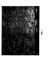
- Figure 7 depicts the as-cast microstructure of a Co-14Cr-12.5Pt-6Cu-12B atomic percent alloy.
- the microstructure consists of a primary dendritic phase (shown as light gray) surrounded by a eutectic matrix (shown as a lamellae-like phase).
- the dendritic phase is a CoPtCu rich phase with a minor amount of dissolved Cr.
- the eutectic matrix is substantially a CrCoB phase.
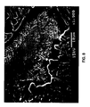
- Figure 8 is an SEM micrograph, or back-scattered electron image, of the grain. The contrast in such images originates from the differences in atomic weight of the various phases' constituents. While the dendritic phase appears to be a single phase, a chemically etched sample revealed the presence of another Cu rich phase. In this regard, Figure 8 shows a high magnification image of a dendrite in which "pits" can be distinguished at the grain boundaries, resulting from the preferential erosion of the Cu 3 Pt-rich phase upon etching.
- the present invention is a magnetic recording medium including a substrate and a data-storing thin film layer formed over the substrate.
- the data-storing thin film layer is comprised of Co, greater than 0 and as much as 24 atomic percent Cr, greater than 0 and as much as 20 atomic percent Pt, greater than 0 and as much as 20 atomic percent B, and greater than 0 and as much as 10 atomic percent X 1 , wherein X 1 is an element selected from the group consisting of Ag, Ce, Cu, Dy, Er, Eu, Gd, Ho, In, La, Lu, Mo, Nd, Pr, Sm, Tl, W, and Yb.
- the present invention is a method for manufacturing a magnetic recording medium.
- the method includes the step of sputtering at least a first data-storing thin film layer over a substrate from a sputter target, where the sputter target is comprised of Co, greater than 0 and as much as 24 atomic percent Cr, greater than 0 and as much as 20 atomic percent Pt, greater than 0 and as much as 20 atomic percent B, and greater than 0 and as much as 10 atomic percent X 1 , where X 1 is an element selected from the group consisting of Ag, Ce, Cu, Dy, Er, Eu, Gd, Ho, In, La, Lu, Mo, Nd, Pr, Sm, Tl, W, and Yb.
Landscapes
- Chemical & Material Sciences (AREA)
- Engineering & Computer Science (AREA)
- Metallurgy (AREA)
- Organic Chemistry (AREA)
- Mechanical Engineering (AREA)
- Materials Engineering (AREA)
- Chemical Kinetics & Catalysis (AREA)
- Physics & Mathematics (AREA)
- Plasma & Fusion (AREA)
- Analytical Chemistry (AREA)
- Manufacturing Of Magnetic Record Carriers (AREA)
- Physical Vapour Deposition (AREA)
- Powder Metallurgy (AREA)
- Magnetic Record Carriers (AREA)
- Thin Magnetic Films (AREA)
Applications Claiming Priority (2)
| Application Number | Priority Date | Filing Date | Title |
|---|---|---|---|
| US866795 | 2004-06-15 | ||
| US10/866,795 US20050277002A1 (en) | 2004-06-15 | 2004-06-15 | Enhanced sputter target alloy compositions |
Publications (2)
| Publication Number | Publication Date |
|---|---|
| EP1607940A2 true EP1607940A2 (fr) | 2005-12-21 |
| EP1607940A3 EP1607940A3 (fr) | 2006-02-15 |
Family
ID=34977102
Family Applications (1)
| Application Number | Title | Priority Date | Filing Date |
|---|---|---|---|
| EP05252880A Withdrawn EP1607940A3 (fr) | 2004-06-15 | 2005-05-11 | Compositions améliorées d'alliages d'un cible à pulvérisation |
Country Status (8)
| Country | Link |
|---|---|
| US (1) | US20050277002A1 (fr) |
| EP (1) | EP1607940A3 (fr) |
| JP (1) | JP2006004611A (fr) |
| KR (1) | KR100776383B1 (fr) |
| CN (1) | CN1712551A (fr) |
| CZ (1) | CZ2005343A3 (fr) |
| SG (1) | SG118324A1 (fr) |
| TW (1) | TW200604363A (fr) |
Cited By (4)
| Publication number | Priority date | Publication date | Assignee | Title |
|---|---|---|---|---|
| EP1637625A2 (fr) * | 2004-09-01 | 2006-03-22 | Heraeus, Inc. | Matériau de cible. |
| EP1715069A1 (fr) * | 2005-04-18 | 2006-10-25 | Heraeus, Inc. | Formulation améliorée d'un composite à matrice à base de cobalt |
| SG140517A1 (en) * | 2006-09-01 | 2008-03-28 | Heraeus Inc | Magnetic media and sputter targets with compositions of high anisotropy alloys and oxide compounds |
| WO2008050644A1 (fr) * | 2006-10-19 | 2008-05-02 | Asahi Glass Company, Limited | Cible de pulvérisation utilisée pour la production d'une ébauche de masque réfléchissant pour lithographie euv |
Families Citing this family (9)
| Publication number | Priority date | Publication date | Assignee | Title |
|---|---|---|---|---|
| JP4377906B2 (ja) | 2006-11-20 | 2009-12-02 | 株式会社コベルコ科研 | Al−Ni−La系Al基合金スパッタリングターゲット、およびその製造方法 |
| JP5139134B2 (ja) * | 2008-03-31 | 2013-02-06 | 株式会社コベルコ科研 | Al−Ni−La−Cu系Al基合金スパッタリングターゲットおよびその製造方法 |
| JP5394577B2 (ja) * | 2010-12-22 | 2014-01-22 | Jx日鉱日石金属株式会社 | 強磁性材スパッタリングターゲット |
| JP5863411B2 (ja) * | 2011-11-17 | 2016-02-16 | 田中貴金属工業株式会社 | マグネトロンスパッタリング用ターゲットおよびその製造方法 |
| JP5646757B2 (ja) * | 2012-01-25 | 2014-12-24 | Jx日鉱日石金属株式会社 | 強磁性材スパッタリングターゲット |
| JP5851582B2 (ja) * | 2012-02-23 | 2016-02-03 | Jx日鉱日石金属株式会社 | クロム酸化物を含有する強磁性材スパッタリングターゲット |
| US9970099B2 (en) | 2012-03-09 | 2018-05-15 | Jx Nippon Mining & Metals Corporation | Sputtering target for magnetic recording medium, and process for producing same |
| SG11201606737UA (en) * | 2014-09-04 | 2016-09-29 | Jx Nippon Mining & Metals Corp | Sputtering target |
| CN115132396B (zh) * | 2022-07-18 | 2025-06-13 | 同济大学 | 一种用于中子自旋翻转器的多层中子薄膜自旋翻转元件及其制作方法 |
Family Cites Families (36)
| Publication number | Priority date | Publication date | Assignee | Title |
|---|---|---|---|---|
| US3147112A (en) * | 1961-01-19 | 1964-09-01 | Du Pont | Ferromagnetic mn-ga alloy and method of production |
| JPH06104120A (ja) * | 1992-08-03 | 1994-04-15 | Hitachi Metals Ltd | 磁気記録媒体用スパッタリングターゲットおよびその製造方法 |
| US5846648A (en) * | 1994-01-28 | 1998-12-08 | Komag, Inc. | Magnetic alloy having a structured nucleation layer and method for manufacturing same |
| JPH0850715A (ja) * | 1994-01-28 | 1996-02-20 | Komag Inc | 低ノイズ,高い保磁力および優れた方形度を有する磁気記録媒体および磁気記録媒体形成方法 |
| US5523173A (en) * | 1994-12-27 | 1996-06-04 | International Business Machines Corporation | Magnetic recording medium with a CoPtCrB alloy thin film with a 1120 crystallographic orientation deposited on an underlayer with 100 orientation |
| JP3544293B2 (ja) * | 1997-07-31 | 2004-07-21 | 株式会社日鉱マテリアルズ | 磁性材用Mn合金材料、Mn合金スパッタリングタ−ゲット及び磁性薄膜 |
| JP3087715B2 (ja) * | 1998-02-19 | 2000-09-11 | 日本電気株式会社 | 磁気ディスク装置 |
| JP4082785B2 (ja) * | 1998-05-15 | 2008-04-30 | 富士通株式会社 | 磁気記録媒体及びその製造方法 |
| AU4431100A (en) * | 1999-05-11 | 2000-11-21 | Hitachi Maxell, Ltd. | Magnetic recording medium and its production method, and magnetic recorder |
| JP2000339635A (ja) * | 1999-05-31 | 2000-12-08 | Toshiba Corp | 磁気ヘッド及び磁気記録再生装置 |
| US6440589B1 (en) * | 1999-06-02 | 2002-08-27 | International Business Machines Corporation | Magnetic media with ferromagnetic overlay materials for improved thermal stability |
| JP2001026860A (ja) * | 1999-07-14 | 2001-01-30 | Hitachi Metals Ltd | Co−Pt−B系ターゲットおよびその製造方法 |
| US6740353B1 (en) * | 1999-09-10 | 2004-05-25 | Tdk Corporation | Process for producing magnetic recording medium |
| JP2001107226A (ja) * | 1999-10-01 | 2001-04-17 | Hitachi Metals Ltd | Co系ターゲットおよびその製造方法 |
| US6620531B1 (en) * | 1999-12-20 | 2003-09-16 | Seagate Technology Llc | Magnetic recording media with oxidized seedlayer for reduced grain size and reduced grain size distribution |
| US6524724B1 (en) * | 2000-02-11 | 2003-02-25 | Seagate Technology Llc | Control of magnetic film grain structure by modifying Ni-P plating of the substrate |
| JP2001236643A (ja) * | 2000-02-23 | 2001-08-31 | Fuji Electric Co Ltd | 磁気記録媒体製造用スパッタリングターゲット、それを用いた磁気記録媒体の製造方法および磁気記録媒体 |
| US6738234B1 (en) * | 2000-03-15 | 2004-05-18 | Tdk Corporation | Thin film magnetic head and magnetic transducer |
| SG91343A1 (en) * | 2000-07-19 | 2002-09-17 | Toshiba Kk | Perpendicular magnetic recording medium and magnetic recording apparatus |
| JP4309075B2 (ja) * | 2000-07-27 | 2009-08-05 | 株式会社東芝 | 磁気記憶装置 |
| US6821653B2 (en) * | 2000-09-12 | 2004-11-23 | Showa Denko Kabushiki Kaisha | Magnetic recording medium, process for producing the same, and magnetic recording and reproducing apparatus |
| JP2002100018A (ja) * | 2000-09-25 | 2002-04-05 | Fujitsu Ltd | 磁気記録媒体及びその製造方法並び磁気記憶装置 |
| US20020106297A1 (en) * | 2000-12-01 | 2002-08-08 | Hitachi Metals, Ltd. | Co-base target and method of producing the same |
| JP2002208125A (ja) * | 2001-01-05 | 2002-07-26 | Hitachi Metals Ltd | Co−Cr−Pt系ターゲット材および磁気記録媒体 |
| JP3993786B2 (ja) * | 2001-06-29 | 2007-10-17 | 富士通株式会社 | 磁気記録媒体 |
| US6723458B2 (en) * | 2001-08-17 | 2004-04-20 | Showa Denko K.K. | Magnetic recording medium, method of manufacture therefor, and magnetic read/write apparatus |
| US6818331B2 (en) * | 2001-08-28 | 2004-11-16 | Showa Denko Kabushiki Kaisha | Magnetic recording medium, production process thereof, and magnetic recording and reproducing apparatus |
| JP4626840B2 (ja) * | 2001-08-31 | 2011-02-09 | 富士電機デバイステクノロジー株式会社 | 垂直磁気記録媒体及びその製造方法 |
| JP2003099911A (ja) * | 2001-09-26 | 2003-04-04 | Fujitsu Ltd | 磁気記録媒体及びその製造方法 |
| US6926977B2 (en) * | 2001-10-22 | 2005-08-09 | Showa Denko Kabushiki Kaisha | Magnetic recording medium, production process thereof, and magnetic recording and reproducing apparatus |
| US6567236B1 (en) * | 2001-11-09 | 2003-05-20 | International Business Machnes Corporation | Antiferromagnetically coupled thin films for magnetic recording |
| JP4157707B2 (ja) * | 2002-01-16 | 2008-10-01 | 株式会社東芝 | 磁気メモリ |
| WO2003075263A1 (fr) * | 2002-02-28 | 2003-09-12 | Seagate Technology Llc | Alliages de cobalt-platine chimiquement ordonnes pour enregistrement magnetique |
| US6723450B2 (en) * | 2002-03-19 | 2004-04-20 | Hitachi Global Storage Technologies Netherlands B.V. | Magnetic recording medium with antiparallel coupled ferromagnetic films as the recording layer |
| US6882834B1 (en) * | 2002-04-26 | 2005-04-19 | Analog Devices, Inc. | Direct conversion receiver apparatus |
| AU2003291159A1 (en) * | 2002-12-09 | 2004-06-30 | Honeywell International Inc. | High purity nickel/vanadium sputtering components; and methods of making sputtering components |
-
2004
- 2004-06-15 US US10/866,795 patent/US20050277002A1/en not_active Abandoned
-
2005
- 2005-05-10 SG SG200502942A patent/SG118324A1/en unknown
- 2005-05-11 EP EP05252880A patent/EP1607940A3/fr not_active Withdrawn
- 2005-05-19 TW TW094116377A patent/TW200604363A/zh unknown
- 2005-05-27 CZ CZ20050343A patent/CZ2005343A3/cs unknown
- 2005-05-31 KR KR1020050046082A patent/KR100776383B1/ko not_active Expired - Fee Related
- 2005-06-10 JP JP2005170316A patent/JP2006004611A/ja active Pending
- 2005-06-15 CN CNA2005100764622A patent/CN1712551A/zh active Pending
Non-Patent Citations (1)
| Title |
|---|
| None * |
Cited By (7)
| Publication number | Priority date | Publication date | Assignee | Title |
|---|---|---|---|---|
| EP1637625A2 (fr) * | 2004-09-01 | 2006-03-22 | Heraeus, Inc. | Matériau de cible. |
| EP1715069A1 (fr) * | 2005-04-18 | 2006-10-25 | Heraeus, Inc. | Formulation améliorée d'un composite à matrice à base de cobalt |
| US7494617B2 (en) | 2005-04-18 | 2009-02-24 | Heraeus Inc. | Enhanced formulation of cobalt alloy matrix compositions |
| SG140517A1 (en) * | 2006-09-01 | 2008-03-28 | Heraeus Inc | Magnetic media and sputter targets with compositions of high anisotropy alloys and oxide compounds |
| WO2008050644A1 (fr) * | 2006-10-19 | 2008-05-02 | Asahi Glass Company, Limited | Cible de pulvérisation utilisée pour la production d'une ébauche de masque réfléchissant pour lithographie euv |
| US7855036B2 (en) | 2006-10-19 | 2010-12-21 | Asahi Glass Company, Limited | Sputtering target used for production of reflective mask blank for EUV lithography |
| KR101317981B1 (ko) | 2006-10-19 | 2013-10-14 | 아사히 가라스 가부시키가이샤 | Euv 리소그래피용 반사형 마스크 블랭크 제조에 사용되는 스퍼터링 타겟 |
Also Published As
| Publication number | Publication date |
|---|---|
| KR100776383B1 (ko) | 2007-11-16 |
| TW200604363A (en) | 2006-02-01 |
| KR20060046315A (ko) | 2006-05-17 |
| EP1607940A3 (fr) | 2006-02-15 |
| JP2006004611A (ja) | 2006-01-05 |
| CZ2005343A3 (cs) | 2006-02-15 |
| US20050277002A1 (en) | 2005-12-15 |
| CN1712551A (zh) | 2005-12-28 |
| SG118324A1 (en) | 2006-01-27 |
Similar Documents
| Publication | Publication Date | Title |
|---|---|---|
| US6846583B2 (en) | Magnetic recording medium and magnetic recording apparatus | |
| US20080131735A1 (en) | Ni-X, Ni-Y, and Ni-X-Y alloys with or without oxides as sputter targets for perpendicular magnetic recording | |
| US20060188743A1 (en) | Fept magnetic thin film having perpendicular magnetic anisotropy and method for preparation thereof | |
| EP1607940A2 (fr) | Compositions améliorées d'alliages d'un cible à pulvérisation | |
| JP2007087575A (ja) | 磁気記録媒体におけるチューニング交換結合 | |
| JP2002334424A (ja) | 磁気記録媒体、その製造方法、および磁気記録再生装置 | |
| EP1746586A1 (fr) | Compositions améliorées d' alliage pour cible de pulvérisation | |
| US7494617B2 (en) | Enhanced formulation of cobalt alloy matrix compositions | |
| Ariake et al. | Co-Pt-TiO/sub 2/composite film for perpendicular magnetic recording medium | |
| US7666529B2 (en) | Anti-ferromagnetically coupled soft underlayer | |
| US20070099032A1 (en) | Deposition of enhanced seed layer using tantalum alloy based sputter target | |
| US20110129692A1 (en) | Magnetic alloy materials with hcp stabilized microstructure, magnetic recording media comprising same, and fabrication method therefor | |
| EP1850334A1 (fr) | Souscouche magnétique douce dans moyen magnétique et cible de pulvérisation en alliage magnétique doux | |
| JP2005521980A (ja) | 磁気記録媒体及び磁気記憶装置 | |
| JP4171732B2 (ja) | 磁気記録媒体及び磁気記憶装置 | |
| JP2004227701A (ja) | 垂直磁気記録媒体 | |
| HK1080600A (en) | Enhanced sputter target alloy compositions | |
| HK1095417A (en) | Enhanced sputter target alloy compositions | |
| JP2007164941A (ja) | 垂直磁気記録媒体 | |
| Sato et al. | Grain diameter and coercivity of Fe, Ni, and Co metals | |
| JP5177407B2 (ja) | 磁気異方性垂直磁化膜及びその形成方法並びに磁気記録媒体及びその製造方法 | |
| JP2009070857A (ja) | 島状磁性薄膜及びその製造方法 | |
| JP3880000B2 (ja) | 高飽和磁束密度軟磁性材料 | |
| JP2011081873A (ja) | 垂直磁気記録媒体用記録層、垂直磁気記録媒体、及び強磁性金属膜の作製方法 | |
| HK1105712A (en) | Soft magnetic underlayer in magnetic media and soft magnetic alloy based sputter target |
Legal Events
| Date | Code | Title | Description |
|---|---|---|---|
| PUAI | Public reference made under article 153(3) epc to a published international application that has entered the european phase |
Free format text: ORIGINAL CODE: 0009012 |
|
| AK | Designated contracting states |
Kind code of ref document: A2 Designated state(s): AT BE BG CH CY CZ DE DK EE ES FI FR GB GR HU IE IS IT LI LT LU MC NL PL PT RO SE SI SK TR |
|
| AX | Request for extension of the european patent |
Extension state: AL BA HR LV MK YU |
|
| PUAL | Search report despatched |
Free format text: ORIGINAL CODE: 0009013 |
|
| AK | Designated contracting states |
Kind code of ref document: A3 Designated state(s): AT BE BG CH CY CZ DE DK EE ES FI FR GB GR HU IE IS IT LI LT LU MC NL PL PT RO SE SI SK TR |
|
| AX | Request for extension of the european patent |
Extension state: AL BA HR LV MK YU |
|
| RIC1 | Information provided on ipc code assigned before grant |
Ipc: C23C 14/34 20060101ALI20051229BHEP Ipc: C22C 19/07 20060101ALI20051229BHEP Ipc: G11B 5/851 20060101ALI20051229BHEP Ipc: G11B 5/64 20060101AFI20050928BHEP |
|
| REG | Reference to a national code |
Ref country code: HK Ref legal event code: DE Ref document number: 1080600 Country of ref document: HK |
|
| 17P | Request for examination filed |
Effective date: 20060411 |
|
| AKX | Designation fees paid |
Designated state(s): DE FR GB |
|
| 17Q | First examination report despatched |
Effective date: 20060602 |
|
| STAA | Information on the status of an ep patent application or granted ep patent |
Free format text: STATUS: THE APPLICATION IS DEEMED TO BE WITHDRAWN |
|
| 18D | Application deemed to be withdrawn |
Effective date: 20070710 |
|
| REG | Reference to a national code |
Ref country code: HK Ref legal event code: WD Ref document number: 1080600 Country of ref document: HK |