EP1608066A1 - Convertisseur continu-continu à haut rendement - Google Patents
Convertisseur continu-continu à haut rendement Download PDFInfo
- Publication number
- EP1608066A1 EP1608066A1 EP04392028A EP04392028A EP1608066A1 EP 1608066 A1 EP1608066 A1 EP 1608066A1 EP 04392028 A EP04392028 A EP 04392028A EP 04392028 A EP04392028 A EP 04392028A EP 1608066 A1 EP1608066 A1 EP 1608066A1
- Authority
- EP
- European Patent Office
- Prior art keywords
- converter
- size
- mosfet
- variable size
- output current
- Prior art date
- Legal status (The legal status is an assumption and is not a legal conclusion. Google has not performed a legal analysis and makes no representation as to the accuracy of the status listed.)
- Ceased
Links
- 238000000034 method Methods 0.000 claims description 13
- 230000007423 decrease Effects 0.000 claims description 4
- 230000003247 decreasing effect Effects 0.000 claims description 2
- 238000010586 diagram Methods 0.000 description 4
- 230000001276 controlling effect Effects 0.000 description 3
- 230000002349 favourable effect Effects 0.000 description 3
- 239000000523 sample Substances 0.000 description 2
- 230000000295 complement effect Effects 0.000 description 1
- 238000007599 discharging Methods 0.000 description 1
- 230000005669 field effect Effects 0.000 description 1
- 239000000463 material Substances 0.000 description 1
- 230000001105 regulatory effect Effects 0.000 description 1
Images



Classifications
-
- H—ELECTRICITY
- H02—GENERATION; CONVERSION OR DISTRIBUTION OF ELECTRIC POWER
- H02M—APPARATUS FOR CONVERSION BETWEEN AC AND AC, BETWEEN AC AND DC, OR BETWEEN DC AND DC, AND FOR USE WITH MAINS OR SIMILAR POWER SUPPLY SYSTEMS; CONVERSION OF DC OR AC INPUT POWER INTO SURGE OUTPUT POWER; CONTROL OR REGULATION THEREOF
- H02M3/00—Conversion of DC power input into DC power output
- H02M3/02—Conversion of DC power input into DC power output without intermediate conversion into AC
- H02M3/04—Conversion of DC power input into DC power output without intermediate conversion into AC by static converters
- H02M3/10—Conversion of DC power input into DC power output without intermediate conversion into AC by static converters using discharge tubes with control electrode or semiconductor devices with control electrode
- H02M3/145—Conversion of DC power input into DC power output without intermediate conversion into AC by static converters using discharge tubes with control electrode or semiconductor devices with control electrode using devices of a triode or transistor type requiring continuous application of a control signal
- H02M3/155—Conversion of DC power input into DC power output without intermediate conversion into AC by static converters using discharge tubes with control electrode or semiconductor devices with control electrode using devices of a triode or transistor type requiring continuous application of a control signal using semiconductor devices only
- H02M3/156—Conversion of DC power input into DC power output without intermediate conversion into AC by static converters using discharge tubes with control electrode or semiconductor devices with control electrode using devices of a triode or transistor type requiring continuous application of a control signal using semiconductor devices only with automatic control of output voltage or current, e.g. switching regulators
- H02M3/158—Conversion of DC power input into DC power output without intermediate conversion into AC by static converters using discharge tubes with control electrode or semiconductor devices with control electrode using devices of a triode or transistor type requiring continuous application of a control signal using semiconductor devices only with automatic control of output voltage or current, e.g. switching regulators including plural semiconductor devices as final control devices for a single load
- H02M3/1584—Conversion of DC power input into DC power output without intermediate conversion into AC by static converters using discharge tubes with control electrode or semiconductor devices with control electrode using devices of a triode or transistor type requiring continuous application of a control signal using semiconductor devices only with automatic control of output voltage or current, e.g. switching regulators including plural semiconductor devices as final control devices for a single load with a plurality of power processing stages connected in parallel
-
- H—ELECTRICITY
- H03—ELECTRONIC CIRCUITRY
- H03K—PULSE TECHNIQUE
- H03K17/00—Electronic switching or gating, i.e. not by contact-making and –breaking
- H03K17/12—Modifications for increasing the maximum permissible switched current
- H03K17/122—Modifications for increasing the maximum permissible switched current in field-effect transistor switches
-
- H—ELECTRICITY
- H02—GENERATION; CONVERSION OR DISTRIBUTION OF ELECTRIC POWER
- H02M—APPARATUS FOR CONVERSION BETWEEN AC AND AC, BETWEEN AC AND DC, OR BETWEEN DC AND DC, AND FOR USE WITH MAINS OR SIMILAR POWER SUPPLY SYSTEMS; CONVERSION OF DC OR AC INPUT POWER INTO SURGE OUTPUT POWER; CONTROL OR REGULATION THEREOF
- H02M1/00—Details of apparatus for conversion
- H02M1/0003—Details of control, feedback or regulation circuits
- H02M1/0032—Control circuits allowing low power mode operation, e.g. in standby mode
-
- H—ELECTRICITY
- H02—GENERATION; CONVERSION OR DISTRIBUTION OF ELECTRIC POWER
- H02M—APPARATUS FOR CONVERSION BETWEEN AC AND AC, BETWEEN AC AND DC, OR BETWEEN DC AND DC, AND FOR USE WITH MAINS OR SIMILAR POWER SUPPLY SYSTEMS; CONVERSION OF DC OR AC INPUT POWER INTO SURGE OUTPUT POWER; CONTROL OR REGULATION THEREOF
- H02M1/00—Details of apparatus for conversion
- H02M1/08—Circuits specially adapted for the generation of control voltages for semiconductor devices incorporated in static converters
- H02M1/088—Circuits specially adapted for the generation of control voltages for semiconductor devices incorporated in static converters for the simultaneous control of series or parallel connected semiconductor devices
-
- Y—GENERAL TAGGING OF NEW TECHNOLOGICAL DEVELOPMENTS; GENERAL TAGGING OF CROSS-SECTIONAL TECHNOLOGIES SPANNING OVER SEVERAL SECTIONS OF THE IPC; TECHNICAL SUBJECTS COVERED BY FORMER USPC CROSS-REFERENCE ART COLLECTIONS [XRACs] AND DIGESTS
- Y02—TECHNOLOGIES OR APPLICATIONS FOR MITIGATION OR ADAPTATION AGAINST CLIMATE CHANGE
- Y02B—CLIMATE CHANGE MITIGATION TECHNOLOGIES RELATED TO BUILDINGS, e.g. HOUSING, HOUSE APPLIANCES OR RELATED END-USER APPLICATIONS
- Y02B70/00—Technologies for an efficient end-user side electric power management and consumption
- Y02B70/10—Technologies improving the efficiency by using switched-mode power supplies [SMPS], i.e. efficient power electronics conversion e.g. power factor correction or reduction of losses in power supplies or efficient standby modes
Definitions
- the present invention relates to switching DC-DC converters, using CMOS switching transistors.
- Fig. 1 shows one conceptual circuit diagram of a buck converter out of a variety of possible implementations of DC-DC converters.
- U. S. Patent 6,462,962 (to Cuk) describes a circuit that implements a lossless switching DC-to-DC converter with lossless switching time control for up to four controllable switches, with each switch meeting the specific current-voltage switching characteristics.
- U. S. Patent 6,487,094 discloses a high efficiency DC-DC power converter, where the voltage across the main switch due to leakage inductance of the transformer is clamped and leakage energy of the transformer is recycled instead of being dissipated so as to improve operating efficiency.
- U. S. Patent 4,859,927 shows a highly efficient switching regulator for a field effect transistor employed in a regulated power supply as the switching element for an unregulated power source, using a pair of complementary control transistors.
- a principal object of the invention is to achieve high energy efficiency for a DC-DC converter at a wide range of converter load currents.
- the disclosed invention changes the size of the switching transistors according to the converter output current, thus combining the efficiency of small transistors at low output currents and of large transistors at high output currents.
- Key elements of the disclosed invention are the one or more means for MOSFET switching transistor arrangements, implementing variable size switching transistors.
- the implementation of said means for MOSFET switching transistor arrangements, implementing variable size switching transistors will allow to change said transistors size under control of a signal provided to each of said means for MOSFET switching transistor arrangement.
- Buck Converters have typically two switching transistors, whereas Boost Converters have typically only one switching transistor.
- Other DC-DC Converters may have one to four switching transistors providing their key power switching function.
- the MOSFET switching transistor arrangements can be of the NMOS or of the PMOS transistor type, i.e. there could be a NMOS switching transistor arrangement, implementing a variable size switching transistor and/or a PMOS switching transistor arrangement, implementing a variable size switching transistor, which shall hereafter be called variable size NMOS switching transistor and variable size PMOS switching transistor. If any type and/or any number of said variable size NMOS switching transistors or variable size PMOS switching transistors is considered, it shall hereafter be called variable size MOSFET switching transistors.
- variable size MOSFET switching transistors To control the size of said variable size MOSFET switching transistors, first appropriate means for sensing a current as a measure for the converter output current take a current probe to provide, with possibly the assistance of additional integrating means, a measure of the converter output current. Then a logical function in the means to generate a control signal, intended to select the desired size of said variable size MOSFET transistors will decide, based on said measure for the converter output current, what size of each of said variable size MOSFET switching transistors to select at a certain point in time. A selection mechanism will activate the appropriate transistor elements to finally realize said variable size MOSFET transistors with the desired size.
- variable size MOSFET switching transistor is to build a set of small transistors, either of the same or of different sizes, to connect them in parallel and to activate or deactivate each individual transistor element according to the desired total size by enabling or disabling them through a logic function placed at the inputs of their gates.
- one possible solution is to make all gates of equal size. Another solution is to produce gates with sizes stepping with binary values (i.e. 1, 2, 4, 8 etc.). A further solution could be to step said gate sizes in a way to provide a nonlinear curve, for example in steps along a logarithmic curve.
- variable size MOSFET transistors In general, it is desirable to provide a proportional relation between the DC-DC converter's output current and the size of said variable size MOSFET switching transistor. Nevertheless the size of said variable size MOSFET transistors will not change in a steady and linear way, it will change stepwise. Required size of the MOSFET transistor for the highest current will define the size and does not add additional area for the MOSFET transistor.
- the method of achieving the goal of improved efficiency of a DC-DC converter is to first provide a measure of the output current of said DC-DC converter; then generating a control signal, based on said output current of said DC-DC converter to change the sizes of said means for said variable size MOSFET transistors; and finally selecting the size of said variable size MOSFET transistors according to said converter output current, i.e. increasing the sizes of said means for variable size MOSFET transistors, when said measure of the output current indicates that said output current of said DC-DC converter increases and decreasing the sizes of said means for variable size MOSFET transistors, when said measure of the output current indicates that said output current of said DC-DC converter decreases.
- a principal object of the invention is to achieve high energy efficiency for a DC-DC converter at a wide range of converter load currents, which can be achieve by reducing the switching losses of the power switching transistors.
- the disclosed invention changes the size of the switching transistors according to the converter output current, thus combining the efficiency of small transistors at low output currents and of large transistors at high output currents.
- Key elements of the disclosed invention are the one or more means for MOSFET switching transistor arrangements, implementing variable size switching transistors.
- the implementation of said means for MOSFET switching transistor arrangements, implementing variable size switching transistors will allow to change said transistors size under control of a signal provided to each of said means for MOSFET switching transistor arrangement.
- Boost Converters have typically one switching transistor
- Buck Converters have typically two switching transistors.
- Other DC-DC Converters may have one to four switching transistors providing their key power switching function.
- MOSFET switching transistor arrangements described in this disclosure can be of the NMOS or of the PMOS transistor type, i.e. the variable size MOSFET switching transistors could be a variable size NMOS switching transistor and/or a variable size PMOS switching transistor.
- an appropriate current sensor takes a current probe to provide, with possibly with the assistance of additional integrating means, a measure of the converter output current. Then a logical control function will decide what size of each of said variable size MOSFET switching transistors to select at a certain point of time.
- variable size MOSFET switching transistor is to build a set of small transistors, either of the same or of different sizes, to connect them in parallel and to activate or deactivate each individual transistor element according to the desired total size by enabling or disabling them through a logic function placed at the inputs of their gates.
- one possible solution is to make all gates of equal size. Another solution is to produce gates with sizes stepping with binary values (i.e. 1, 2, 4, 8 etc.). A further solution could be to step said gate sizes in a way to provide a nonlinear curve, for example in steps along a logarithmic curve.
- the comparator takes the signal from preamplifier (PreAmp), the current sensor (CurrSens) and the error amplifier (ErrAmp), and feeds the result to the switch control (SwContr), which then drives the power switching transistors (Sw 11) and (Sw 12).
- PreAmp preamplifier
- Current sensor Current sensor
- ErrAmp error amplifier
- SwContr switch control
- Sw 11 power switching transistors
- Sw 11 power switching transistors
- Sw 12 power switching transistors
- Essential element is always the power switching transistors, typically with one or two such switches.
- each of the power switching transistors are replaced by a MOSFET switching transistor arrangements, implementing variable size switching transistors, as presented in the basic concept drawing of Fig. 2.
- the variable size MOSFET switching transistors are represented by the variable size NMOS switching transistor (Sw 21) and the variable size PMOS switching transistor (Sw 22).
- the actual size of said variable size MOSFET switching transistors is controlled through a size controlling function (SizeCtrl), based on said measure of the converter output current, taken from the current sensor (CurrSens).
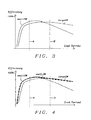
- Fig. 3 shows the efficiency depending on the converter output current. For small switching transistors, the efficiency follows the curve small SW, for large transistors, efficiency follows the large SW line. Below the dotted line (A), efficiency primarily depends on the quiescent current of the switching transistor, between lines (A) and (B), charging/discharging the gate is most important and above line (B) the ohmic loss in the power switching transistor is the dominant factor.
- Fig 5 and Fig 6 show the principal concept of a variety of possible implementations on chip level.
- Fig. 5a visualizes the concept of the parallel connection of individual transistors with equal gate sizes.
- Fig. 5b is similar, but demonstrates different gate sizes, realizing steps in a binary fashion.
- S11 to S14 are the source contacts and D11 to D14 are the drain contacts.
- G11 to G14 are the gates with equal size of the variable size MOSFET switching transistor in Fig. 5a;
- G21 to G24 are the gates in Fig. 5b with sizes of the variable size MOSFET switching transistor, stepping in a binary fashion.
- Fig. 6a and 6b combine the parallel transistors in a single source region and single drain region, to reduce the space requirement on chip.
- S21 to S24 are the source contacts and D21 to D24 are the drain contacts.
- G11 to G14 are the gates with equal size of the variable size MOSFET switching transistor in Fig. 6a; G21 to G24 are the gates in Fig. 6b with sizes of the variable size MOSFET switching transistor, stepping in a binary fashion.
- the total size of all portions of said MOSFET switching transistor arrangement is the same size, as it would be for a single MOSFET transistor, designed for the highest output current of said DC-DC converter; the size controlling mechanism either selects the total size of said MOSFET switching transistor arrangement or a fraction thereof.
- variable size switching transistors variable size switching transistors
- the combined gate (cGate), combined source (cSource) and combined drain (cDrain) build the equivalent gate, source and drain connections.
- the active size of said variable size MOSFET switching transistor is controlled by a selection mechanism, the size control function (SizeCtrl 7), selecting the desired active size of said MOSFET switching transistor arrangement through the control inputs (S-sel).
- the method to improve the efficiency of a DC-DC converter provides the means for the basic circuit functions for a DC-DC converter, for example for a buck converter, the means for a NMOS transistor with variable size; means for a PMOS transistor with variable size; means for a current sensor; means to provide a size selecting control signal, based on the current sensor's result; and means for a controlling function, to change the size of the NMOS/PMOS switching transistors, depending on the actual converter output current (80).
- the method first senses the switching transistor's current (81) as an indirect measure for the converter output current and then integrates (82) the switching transistor's current over several switching cycles, typically over 1 to 50 cycles.
- the selecting mechanism decides on the best switching transistor size (85) to get higher efficiency at a lower converter output current and generates a control signal to decrease the switching transistor size. Or, if said output current significantly increases (84), the selecting mechanism decides on the best switching transistor size (87) to get higher efficiency at a higher converter output current and generates a control signal to increase the switching transistor size. Finally, the optimized size of said MOSFET switching transistor arrangement is selected and activated (86)(88).
Landscapes
- Engineering & Computer Science (AREA)
- Power Engineering (AREA)
- Dc-Dc Converters (AREA)
Priority Applications (1)
| Application Number | Priority Date | Filing Date | Title |
|---|---|---|---|
| EP04392028A EP1608066A1 (fr) | 2004-06-14 | 2004-06-14 | Convertisseur continu-continu à haut rendement |
Applications Claiming Priority (1)
| Application Number | Priority Date | Filing Date | Title |
|---|---|---|---|
| EP04392028A EP1608066A1 (fr) | 2004-06-14 | 2004-06-14 | Convertisseur continu-continu à haut rendement |
Publications (1)
| Publication Number | Publication Date |
|---|---|
| EP1608066A1 true EP1608066A1 (fr) | 2005-12-21 |
Family
ID=34931984
Family Applications (1)
| Application Number | Title | Priority Date | Filing Date |
|---|---|---|---|
| EP04392028A Ceased EP1608066A1 (fr) | 2004-06-14 | 2004-06-14 | Convertisseur continu-continu à haut rendement |
Country Status (1)
| Country | Link |
|---|---|
| EP (1) | EP1608066A1 (fr) |
Cited By (7)
| Publication number | Priority date | Publication date | Assignee | Title |
|---|---|---|---|---|
| EP2309629A1 (fr) * | 2009-10-09 | 2011-04-13 | Dialog Semiconductor GmbH | Pompe à charge fractionnelle VDD/5 ou VDD/6 |
| EP2615731A1 (fr) * | 2012-01-11 | 2013-07-17 | Research In Motion Limited | Convertisseur CC/CC avec modules de convertisseur pouvant être activés ou désactivés dynamiquement |
| US8786264B2 (en) | 2012-01-11 | 2014-07-22 | Blackberry Limited | DCDC converter with converter modules that can be dynamically enabled or disabled |
| WO2014116867A1 (fr) * | 2013-01-28 | 2014-07-31 | Qualcomm Incorporated | Mise à l'échelle de commutateur dynamique pour des convertisseurs de puissance en mode commuté |
| EP2892140A1 (fr) * | 2014-01-03 | 2015-07-08 | Apple Inc. | Chargeur de batterie à efficacité élevée |
| US9550421B2 (en) | 2014-03-17 | 2017-01-24 | Denso International America, Inc. | DC-to-DC converter with variable set-point control |
| WO2019217372A1 (fr) * | 2018-05-07 | 2019-11-14 | The Regents Of The University Of Colorado, A Body Corporate | Modulation d'alimentation d'amplificateur de puissance rf multiniveau à alimentation unique |
Citations (5)
| Publication number | Priority date | Publication date | Assignee | Title |
|---|---|---|---|---|
| JPH1094246A (ja) | 1996-08-28 | 1998-04-10 | Samsung Electron Co Ltd | 力率補償電源装置 |
| US5801572A (en) | 1995-02-24 | 1998-09-01 | Nec Corporation | Power MOSFET |
| US5969514A (en) | 1997-11-24 | 1999-10-19 | National Semiconductor Corporation | Digital feedback power supply |
| US6353543B2 (en) | 1999-09-16 | 2002-03-05 | Tdk Corporation | Switching circuit of power conversion apparatus |
| US20030038615A1 (en) | 2001-08-23 | 2003-02-27 | Fairchild Semiconductor Corporation | Method and circuit for reducing losses in DC-DC converters |
-
2004
- 2004-06-14 EP EP04392028A patent/EP1608066A1/fr not_active Ceased
Patent Citations (5)
| Publication number | Priority date | Publication date | Assignee | Title |
|---|---|---|---|---|
| US5801572A (en) | 1995-02-24 | 1998-09-01 | Nec Corporation | Power MOSFET |
| JPH1094246A (ja) | 1996-08-28 | 1998-04-10 | Samsung Electron Co Ltd | 力率補償電源装置 |
| US5969514A (en) | 1997-11-24 | 1999-10-19 | National Semiconductor Corporation | Digital feedback power supply |
| US6353543B2 (en) | 1999-09-16 | 2002-03-05 | Tdk Corporation | Switching circuit of power conversion apparatus |
| US20030038615A1 (en) | 2001-08-23 | 2003-02-27 | Fairchild Semiconductor Corporation | Method and circuit for reducing losses in DC-DC converters |
Non-Patent Citations (1)
| Title |
|---|
| PATENT ABSTRACTS OF JAPAN vol. 1998, no. 09 31 July 1998 (1998-07-31) * |
Cited By (13)
| Publication number | Priority date | Publication date | Assignee | Title |
|---|---|---|---|---|
| US8044707B2 (en) | 2009-10-09 | 2011-10-25 | Dialog Semiconductor Gmbh | VDD/5 or VDD/6 charge-pump |
| EP2309629A1 (fr) * | 2009-10-09 | 2011-04-13 | Dialog Semiconductor GmbH | Pompe à charge fractionnelle VDD/5 ou VDD/6 |
| EP2615731A1 (fr) * | 2012-01-11 | 2013-07-17 | Research In Motion Limited | Convertisseur CC/CC avec modules de convertisseur pouvant être activés ou désactivés dynamiquement |
| US8786264B2 (en) | 2012-01-11 | 2014-07-22 | Blackberry Limited | DCDC converter with converter modules that can be dynamically enabled or disabled |
| US9601999B2 (en) | 2013-01-28 | 2017-03-21 | Qualcomm Incorporated | Dynamic switch scaling for switched-mode power converters |
| WO2014116867A1 (fr) * | 2013-01-28 | 2014-07-31 | Qualcomm Incorporated | Mise à l'échelle de commutateur dynamique pour des convertisseurs de puissance en mode commuté |
| US8988059B2 (en) | 2013-01-28 | 2015-03-24 | Qualcomm Incorporated | Dynamic switch scaling for switched-mode power converters |
| EP2892140A1 (fr) * | 2014-01-03 | 2015-07-08 | Apple Inc. | Chargeur de batterie à efficacité élevée |
| US9444281B2 (en) | 2014-01-03 | 2016-09-13 | Apple Inc. | Unified high power and low power battery charger |
| CN104779659A (zh) * | 2014-01-03 | 2015-07-15 | 苹果公司 | 统一的高电力和低电力电池充电器 |
| US10305305B2 (en) | 2014-01-03 | 2019-05-28 | Apple Inc. | Unified high power and low power battery charger |
| US9550421B2 (en) | 2014-03-17 | 2017-01-24 | Denso International America, Inc. | DC-to-DC converter with variable set-point control |
| WO2019217372A1 (fr) * | 2018-05-07 | 2019-11-14 | The Regents Of The University Of Colorado, A Body Corporate | Modulation d'alimentation d'amplificateur de puissance rf multiniveau à alimentation unique |
Similar Documents
| Publication | Publication Date | Title |
|---|---|---|
| US10594215B2 (en) | Circuits and methods to linearize conversion gain in a DC-DC converter | |
| CN110365208B (zh) | 高效降压-升压电荷泵及其方法 | |
| US9742266B2 (en) | Charge pump timing control | |
| US7808299B2 (en) | Switching power converter with reduced switching losses | |
| US7411379B2 (en) | Apparatus and method for over-voltage and over-current protection for a step-up current-mode converter | |
| US8000113B2 (en) | Efficient power regulation for class-E amplifiers | |
| US7876080B2 (en) | Power converter with monotonic turn-on for pre-charged output capacitor | |
| US7701189B2 (en) | Dynamic gate drive voltage adjustment | |
| US7679342B2 (en) | Power converter with power switch operable in controlled current mode | |
| KR20170068514A (ko) | 펄스식 선형 전력 컨버터 | |
| KR101443583B1 (ko) | 출력 전압을 조절하는 방법 | |
| US7015678B2 (en) | Efficiency improvement of DC-DC converter | |
| GB2311629A (en) | Constant on-time architecture for switching voltage regulator | |
| CN110875686B (zh) | 电子转换器和操作电子转换器的方法 | |
| JP2004096982A (ja) | Dc−dcコンバータ | |
| EP2343794B1 (fr) | Limiteur de courant variable, alimentation électrique et convertisseur de point de charge utilisant le limiteur et procédé de fonctionnement d'un convertisseur de tension non isolé | |
| US20080061757A1 (en) | Output load adaptable mosfet gate drive voltage level in a dc-dc controller | |
| US20120098514A1 (en) | Current mode switching regulator and control circuit and control method thereof | |
| JPH06168043A (ja) | ハイブリッドリニアスイッチング電源 | |
| CN108306489A (zh) | 升降压开关变换器的驱动电路、控制电路及驱动方法 | |
| US20080238380A1 (en) | Hierarchical control for an integrated voltage regulator | |
| US20080238382A1 (en) | Anti-ringing switching regulator and control method therefor | |
| JP2004289993A (ja) | スイッチ・モード電源の制御方法 | |
| EP1952213B1 (fr) | Convertisseur c.c.-c.c. simple | |
| EP1608066A1 (fr) | Convertisseur continu-continu à haut rendement |
Legal Events
| Date | Code | Title | Description |
|---|---|---|---|
| PUAI | Public reference made under article 153(3) epc to a published international application that has entered the european phase |
Free format text: ORIGINAL CODE: 0009012 |
|
| AK | Designated contracting states |
Kind code of ref document: A1 Designated state(s): AT BE BG CH CY CZ DE DK EE ES FI FR GB GR HU IE IT LI LU MC NL PL PT RO SE SI SK TR |
|
| AX | Request for extension of the european patent |
Extension state: AL HR LT LV MK |
|
| 17P | Request for examination filed |
Effective date: 20060621 |
|
| AKX | Designation fees paid |
Designated state(s): AT BE BG CH CY CZ DE DK EE ES FI FR GB GR HU IE IT LI LU MC NL PL PT RO SE SI SK TR |
|
| 17Q | First examination report despatched |
Effective date: 20070820 |
|
| STAA | Information on the status of an ep patent application or granted ep patent |
Free format text: STATUS: THE APPLICATION HAS BEEN REFUSED |
|
| 18R | Application refused |
Effective date: 20141130 |