EP1608069A2 - Verfahren zur Steuerung eines Analogschalters - Google Patents
Verfahren zur Steuerung eines Analogschalters Download PDFInfo
- Publication number
- EP1608069A2 EP1608069A2 EP05105121A EP05105121A EP1608069A2 EP 1608069 A2 EP1608069 A2 EP 1608069A2 EP 05105121 A EP05105121 A EP 05105121A EP 05105121 A EP05105121 A EP 05105121A EP 1608069 A2 EP1608069 A2 EP 1608069A2
- Authority
- EP
- European Patent Office
- Prior art keywords
- voltage
- transistor
- gate
- vin
- vdd
- Prior art date
- Legal status (The legal status is an assumption and is not a legal conclusion. Google has not performed a legal analysis and makes no representation as to the accuracy of the status listed.)
- Granted
Links
Images


Classifications
-
- H—ELECTRICITY
- H03—ELECTRONIC CIRCUITRY
- H03K—PULSE TECHNIQUE
- H03K17/00—Electronic switching or gating, i.e. not by contact-making and –breaking
- H03K17/16—Modifications for eliminating interference voltages or currents
- H03K17/161—Modifications for eliminating interference voltages or currents in field-effect transistor switches
- H03K17/165—Modifications for eliminating interference voltages or currents in field-effect transistor switches by feedback from the output circuit to the control circuit
-
- G—PHYSICS
- G11—INFORMATION STORAGE
- G11C—STATIC STORES
- G11C27/00—Electric analogue stores, e.g. for storing instantaneous values
- G11C27/02—Sample-and-hold arrangements
- G11C27/024—Sample-and-hold arrangements using a capacitive memory element
Definitions
- the invention relates to the field of analog electronics, and in particular a method of control of an analog switch for reduction the harmonic distortion error due to the injection loads.
- This signal distortion is quantified by its harmonic distortion.
- the conductance (and therefore the dimensions) of the input switches is based on the time on the maximum value of the input signal and on its frequency as opposed to internal switches whose conductance is based on the sole value maximum signal.
- the "Clock-doubling”, or technique of doubling the clock which doubles the value of the voltage clock, to mitigate the end of charge error by increasing the conductance of the switches input.
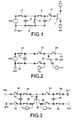
- Such a device implements abilities 2, 4.
- these two Capacities are loaded at Vdd by closing switches 6, 8, 12.
- the reinforcement bottom of one is connected to the armature superior of the other, by closing the switch 10, thereby forming a loaded serial capacitance at a voltage 2Vdd.
- a capacity 20 is charged during a first phase (by closing switches 24 and 26) and is applied to the gate / source terminals of a transistor 22 during a second phase (by closing switches 32 and 34), during which it acts like a battery.
- the transistor 28 is closed: the gate of transistor 22 is at ground or GND potential.
- CMOS complementary polarities
- the proposed invention reduces the harmonic distortion introduced by a switch analogue, including a transistor, for example example of MOS type.
- the first voltage can be equal to Vin + V1
- the second voltage can be equal to Vin + V2.
- the first voltage can be equal to Vin - V1, while the second voltage may be equal to Vin - V2.
- the first potential and the second potential can be fixed potentials or constant.
- the first potential V1 can be higher at the threshold voltage of said transistor.
- the first potential V1 can be also positive.
- the second potential V2 can be less than the threshold voltage of said transistor.
- Vdd can be a voltage greater than the threshold voltage of the transistor.
- the voltage Vdd can to be a bias voltage or a voltage authorized by the technological sector of the transistor.
- the invention also relates to a method of controlling an analog switch having a transistor, to which a Vin input voltage, in which method is applied to the transistor a clock signal, or a signal of grid or control, symmetrical with respect to the input voltage.
- the first voltage Vin + Vdd can be applied, during the first phase, by application a first capacitor charged to Vdd, between the gate and a Vin input voltage or a potential node Wine.
- the second voltage Vin-Vdd can be applied, during the second phase, by applying a second capacitor charged at -Vdd, between the gate and the input voltage Vin, or a node at the potential Vin, or the output voltage V ST .
- the second capacitor can recharge during the first phase, the first capacitor recharging during the second phase.
- the first voltage can be applied by switching of at least one switch.
- the second voltage can be applied by switching of at least one switch.
- the first capacitor can be charged to from a voltage source Vdd from which it is isolated, being discharged, by a transistor whose gate is connected to the transistor gate of the switch analog.
- This transistor can be in the off state when the transistor gate of the switch analog is in the high state and in the on state when the transistor gate of the switch analog is in the low state.
- the second tension is preferably applied via a floating-body or n-type transistor (n> 2) caissons.
- the second capacitor can be connected to the mass from which it is isolated, being discharged, by a transistor whose gate is connected to the gate of the transistor of the analog switch.
- the transistor can be in the off state when the transistor gate of the switch analogue is in the low state and in the on state when the transistor gate of the switch analog is in the high state.
- the first voltage can be equal to Vin + V1
- the second voltage can be equal to Vin + V2.
- the first voltage can be equal to Vin - V1
- the second voltage can be equal to Vin - V2.
- the first potential V1 and the second potential V2 can be fixed potentials or constant.
- the first potential V1 can be positive and greater than the threshold voltage of said transistor.
- the second potential V2 can be less than the threshold voltage of said transistor.
- the voltage Vdd may be greater than the threshold voltage of the transistor.
- the voltage Vdd can to be a bias voltage or a voltage authorized by the technological sector of the transistor.
- a first capacitor can allow to apply the first voltage Vin + Vdd, during the first phase, between the gate and the input voltage Wine.
- a second capacitor can make it possible to apply the second voltage Vin-Vdd, during the second phase, between the gate and the input voltage Vin, or the output voltage V ST .
- Means can reload the second capacitor during the first phase and other means can be used to recharge the first capacitor during the second phase.
- the device comprises at least a switch to apply the first voltage.
- it comprises a source of voltages Vdd to charge the first capacitor and means for isolating, in the course of discharge, the voltage source of the first capacitor.
- Means can be provided to isolate, being discharged, the voltage source of the first capacitor.
- These means comprise for example a transistor whose gate is connected to the gate of the transistor of the analog switch.
- Said transistor can be in the off state when the transistor gate of the switch analogue is in the high state and in the on state when the transistor gate of the switch analog is in the low state.
- a transistor with a body floating or n (n> 2) boxes allows to apply the second voltage.
- the second capacitor can be connected to the mass from which it is isolated, being discharged, by a transistor whose gate is connected to the gate of the transistor of the analog switch.
- Said transistor can be in the off state when the transistor gate of the switch analogue is in the low state and in the on state when the transistor gate of the analog switch is in the high state.
- This circuit improves linearity switches, despite the injection error of charge, thanks to a new clock principle, more symmetrical with respect to the signal.
- gate of a transistor 50 in particular of the MOS type: during a first phase, a first voltage, dependent or function of a Vin input voltage and of a first potential V1, the first voltage being adapted to make said transistor passing. Then, we applied to the transistor gate, during a second phase, a second voltage, dependent or function of the input voltage Vin and a second potential V2, the second voltage being able to block said transistor, the difference between the first voltage and the second voltage being independent of the Vin input voltage.
- the charge injection at the level of the transistor can be made thus more independent of the input signal.
- the transistor 50 can be for example a N-type transistor.
- the first voltage can be equal to wine + V1, while the second voltage can to be equal to wine + V2.
- the first potential V1 and the second potential V2 can be fixed potentials or constant.
- the first potential V1 can be higher at the threshold voltage of said transistor.
- the first potential V1 can be also positive.
- the second potential V2 may be lower than the threshold voltage said transistor.
- a transistor 50 for example of the NMOS type, symmetrical voltages, with respect to a voltage Vin input of a transistor switch, during a first phase and then during a second phase.
- the Vin input voltage comes through example of a microphone, a telephone line type ADSL or a radio frequency reception channel.
- a voltage equal to Vin + Vdd is applied during a first phase, or "on” state, and a voltage equal to Vin - Vdd is applied during a second phase, or “off” state.
- a capacitor 42 originally charged to Vdd, (by closing switches 46 and 62) is applied between the grid 51 of transistor 50 and Vin (by closing switches 48 and 60).
- a voltage equal to Vdd + Vin is then applied to this grid 51.
- a second capacitor 44 is charging at the voltage -Vdd (by closing switches 54 and 56).
- the first capacitor recharges (the switches 48 and 60 are open and the switches 46 and 62 closed) while the capacitor 44 is applied between the gate and the drain of the transistor 50, but with a voltage of opposite sign at first.
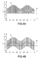
- Figures 4A and 4B show several cycles of charging and discharging a capacitance by a analog switch by a sinusoidal signal, the bottom graph ( Figure 4B) corresponding to a case symmetrical, according to the invention, that of the top (FIG. 4A) in the known "clock-boosting" case.
- Figure 5 illustrates an embodiment of a circuit according to the invention.
- This circuit makes it possible to generate clocks up to + 2Vdd and -Vdd from a Vdd power supply.
- a capacity 70 is applied between the input 72 and the gate 74 via transistors 76, and 78, 80 which form a switch in MOS structures with complementary polarities.
- the negative armature of the capacity 70 is connected to input 72 (at voltage Vin) and its positive frame to grid 74.
- the transistor 82 which, with the transistor 83, allows the capacity 90 to be loaded at Vdd, could start to drive since its source goes up to a voltage higher than its gate.
- a transistor 84 is put in series on this node.
- This transistor whose gate is connected at the gate 74, isolates the voltage source at Vdd of the gate 74, when the latter is in the state high. It is passing when the gate 74 is in the state low.
- transistors 86 and 88 charge the capacitor 90 to a voltage Vdd.
- transistors 76, and 78, 80 are cut and thus isolate the capacity of the grid 74.
- the transistors 92, 94 become passing and connect the positive armature of the capacity 90 to Vin signal.
- the transistor 86 can be found with a positive gate-source voltage, start drive and thus unload capacity 90 in the mass.
- the transistors 82 and 83 are passers to recharge the losses of capacity 70.
- the transistors 96 and 92, 94 are cut, thus insulating the capacity 90 of the grid 74.
- the negative armature of the capacity 90 is connected to the gate 74 by the transistor 96.
- This voltage can be close to -Vdd in the case where Vin is close to 0; in this case, the source / substrate diode of the transistor 96 can be in direct contact, which prevents the node 74 from going below -V diode .
- SOI technologies solve this problem because of the complete isolation of the body and thus make possible this generation of tensions negative orders.
- a transistor 96 with floating body In particular, a transistor 96 with floating body.
- Figures 7 and 8 illustrate the principle source / substrate isolation, respectively for SOI and triple box technologies.
- any voltage less than the mass minus a threshold of diode makes one of these diodes pass.
- This external box contains another 155 P-doped caisson allowing the constitution of a N-type MOS transistor.
- This construction makes it possible to obtain reverse diode box / substrate that prevents the effusion of a negative voltage in the mass of the substrate.
- Figures 9A-9C summarize the different gate voltage principles of the transistor switch: from left to right are represented on principle of a standard gate voltage (FIG. 9A), the principle of a gate voltage with a clock-boosting (Figure 9B) and finally the principle of gate voltage with symmetrical clock-boosting (Figure 9C).
- the voltage Vin is represented in dashed.
- the signal or the gate or gate voltage command constitutes the clock signal.
- Figure 10 shows results of a simulation respectively for a process according to the invention, in symmetrical clock-boosting (curve I) and that of non-symmetrical clock-boosting (curve II).
- the minimum of distortion is also improved, about 10dB.
- the invention allows the improvement of the linearity of analog switches and thus allows improving the performance of these components used in many areas including, in particular, telecommunication applications, analog digital converters and circuits to switched capabilities.
- the invention is not limited to control of N-type transistors and can apply to P-type transistors, in particular to PMOS type transistors.
Landscapes
- Electronic Switches (AREA)
- Oscillators With Electromechanical Resonators (AREA)
- Keying Circuit Devices (AREA)
- Vehicle Waterproofing, Decoration, And Sanitation Devices (AREA)
Applications Claiming Priority (2)
| Application Number | Priority Date | Filing Date | Title |
|---|---|---|---|
| FR0451266A FR2871630B1 (fr) | 2004-06-11 | 2004-06-11 | Procede de commande d'un interrupteur analogique |
| FR0451266 | 2004-06-11 |
Publications (3)
| Publication Number | Publication Date |
|---|---|
| EP1608069A2 true EP1608069A2 (de) | 2005-12-21 |
| EP1608069A3 EP1608069A3 (de) | 2006-04-26 |
| EP1608069B1 EP1608069B1 (de) | 2007-08-08 |
Family
ID=34940145
Family Applications (1)
| Application Number | Title | Priority Date | Filing Date |
|---|---|---|---|
| EP05105121A Expired - Lifetime EP1608069B1 (de) | 2004-06-11 | 2005-06-10 | Verfahren zur Steuerung eines Analogschalters |
Country Status (5)
| Country | Link |
|---|---|
| US (1) | US7274222B2 (de) |
| EP (1) | EP1608069B1 (de) |
| AT (1) | ATE369658T1 (de) |
| DE (1) | DE602005001896T2 (de) |
| FR (1) | FR2871630B1 (de) |
Cited By (1)
| Publication number | Priority date | Publication date | Assignee | Title |
|---|---|---|---|---|
| ES2478791A1 (es) * | 2013-01-22 | 2014-07-22 | Universitat De Les Illes Balears | Interruptor con resistencia modificable |
Families Citing this family (12)
| Publication number | Priority date | Publication date | Assignee | Title |
|---|---|---|---|---|
| EP2080273B1 (de) * | 2006-11-10 | 2018-09-05 | Skyworks Solutions, Inc. | Kompakter verlustarmer hochfrequenzschalter mit verbesserter linearitäts-performance |
| US7710164B1 (en) * | 2007-06-18 | 2010-05-04 | Intersil Americas Inc. | Highly linear bootstrapped switch with improved reliability |
| US20090039924A1 (en) * | 2007-08-09 | 2009-02-12 | Alfio Zanchi | Systems and methods for reducing distortion in semiconductor based sampling systems |
| US8183890B1 (en) | 2008-09-10 | 2012-05-22 | Marvell International Ltd. | Method and apparatus for sampling |
| US8030974B1 (en) | 2008-09-10 | 2011-10-04 | Marvell International, Ltd. | Method and apparatus for sampling |
| US7940091B1 (en) * | 2009-03-02 | 2011-05-10 | Linear Technology Corporation | Bootstrapped switch for sampling voltages beyond the supply voltage |
| US8289066B2 (en) * | 2009-12-30 | 2012-10-16 | Stmicroelectronics Asia Pacific Pte Ltd. | Gate control circuit for high bandwidth switch design |
| FR2968808A1 (fr) * | 2010-12-08 | 2012-06-15 | Commissariat Energie Atomique | Circuit électronique a architecture neuromorphique |
| US8593181B2 (en) * | 2011-08-04 | 2013-11-26 | Analog Devices, Inc. | Input switches in sampling circuits |
| US8525574B1 (en) * | 2012-05-15 | 2013-09-03 | Lsi Corporation | Bootstrap switch circuit with over-voltage prevention |
| EP3429080A1 (de) * | 2017-07-14 | 2019-01-16 | Fraunhofer-Gesellschaft zur Förderung der angewandten Forschung e.V. | Schaltvorrichtung zum schalten eines analogen elektrischen eingangssignals |
| TWI774564B (zh) * | 2021-09-23 | 2022-08-11 | 瑞昱半導體股份有限公司 | 靴帶式開關 |
Family Cites Families (16)
| Publication number | Priority date | Publication date | Assignee | Title |
|---|---|---|---|---|
| US6064872A (en) * | 1991-03-12 | 2000-05-16 | Watkins-Johnson Company | Totem pole mixer having grounded serially connected stacked FET pair |
| US6072353A (en) * | 1995-04-26 | 2000-06-06 | Matsushita Electric Industrial Co., Ltd. | Logic circuit with overdriven off-state switching |
| US6052000A (en) * | 1997-04-30 | 2000-04-18 | Texas Instruments Incorporated | MOS sample and hold circuit |
| JP3613940B2 (ja) * | 1997-08-29 | 2005-01-26 | ソニー株式会社 | ソースフォロワ回路、液晶表示装置および液晶表示装置の出力回路 |
| US5945872A (en) * | 1997-11-06 | 1999-08-31 | Analog Devices, Inc. | Two-phase boosted CMOS switch drive technique and circuit |
| FR2793970B1 (fr) * | 1999-05-20 | 2001-08-31 | St Microelectronics Sa | Procede de commande d'un commutateur d'un dispositif de capacite commutee, et dispositif de capacite commutee correspondant |
| US6310565B1 (en) * | 2000-02-03 | 2001-10-30 | Lucent Technologies Inc. | Sampling switch having an independent “on” impedance |
| US6323697B1 (en) * | 2000-06-06 | 2001-11-27 | Texas Instruments Incorporated | Low distortion sample and hold circuit |
| EP1168619A1 (de) * | 2000-06-19 | 2002-01-02 | STMicroelectronics S.r.l. | Schaltvorrichtung mit erhöhter Steuerung für einen Abtaster eines Analog/Digital-Wandlers, und dessen Betriebsverfahren |
| US6522187B1 (en) * | 2001-03-12 | 2003-02-18 | Linear Technology Corporation | CMOS switch with linearized gate capacitance |
| US6833753B2 (en) * | 2002-11-27 | 2004-12-21 | Texas Instruments Incorporated | Method and system for signal dependent boosting in sampling circuits |
| US7053692B2 (en) * | 2002-12-19 | 2006-05-30 | United Memories, Inc. | Powergate control using boosted and negative voltages |
| US6956411B1 (en) * | 2003-03-27 | 2005-10-18 | National Semiconductor Corporation | Constant RON switch circuit with low distortion and reduction of pedestal errors |
| DE60308346D1 (de) * | 2003-07-03 | 2006-10-26 | St Microelectronics Srl | Mit Spannungserhöhung betriebene Abtastschaltung und zugehöriges Ansteuerverfahren |
| JP2007501483A (ja) * | 2003-08-04 | 2007-01-25 | コーニンクレッカ フィリップス エレクトロニクス エヌ ヴィ | トラック/ホールド回路 |
| JP4128545B2 (ja) * | 2004-05-20 | 2008-07-30 | 富士通株式会社 | サンプリングスイッチ |
-
2004
- 2004-06-11 FR FR0451266A patent/FR2871630B1/fr not_active Expired - Fee Related
-
2005
- 2005-06-10 AT AT05105121T patent/ATE369658T1/de not_active IP Right Cessation
- 2005-06-10 DE DE602005001896T patent/DE602005001896T2/de not_active Expired - Lifetime
- 2005-06-10 US US11/149,216 patent/US7274222B2/en not_active Expired - Fee Related
- 2005-06-10 EP EP05105121A patent/EP1608069B1/de not_active Expired - Lifetime
Cited By (1)
| Publication number | Priority date | Publication date | Assignee | Title |
|---|---|---|---|---|
| ES2478791A1 (es) * | 2013-01-22 | 2014-07-22 | Universitat De Les Illes Balears | Interruptor con resistencia modificable |
Also Published As
| Publication number | Publication date |
|---|---|
| ATE369658T1 (de) | 2007-08-15 |
| US7274222B2 (en) | 2007-09-25 |
| DE602005001896T2 (de) | 2008-05-15 |
| EP1608069A3 (de) | 2006-04-26 |
| FR2871630B1 (fr) | 2007-02-09 |
| FR2871630A1 (fr) | 2005-12-16 |
| DE602005001896D1 (de) | 2007-09-20 |
| EP1608069B1 (de) | 2007-08-08 |
| US20050275448A1 (en) | 2005-12-15 |
Similar Documents
| Publication | Publication Date | Title |
|---|---|---|
| EP2047476B1 (de) | Ladungszurückhaltungsschaltung zur zeitmessung | |
| EP2047475B1 (de) | Schaltung zur auslesung eines ladungszurückhaltungselements zur zeitmessung | |
| EP2050098B1 (de) | Eeprom-ladungserhaltungsschaltung für zeitmessung | |
| EP1608069B1 (de) | Verfahren zur Steuerung eines Analogschalters | |
| EP2047477B1 (de) | Programmierung einer ladungszurückhaltungsschaltung zur zeitmessung | |
| TW201135921A (en) | Pseudo-inverter circuit on SeOI | |
| EP2240956B1 (de) | EEPROM-Zelle mit Ladungsverlust und Herstellungsverfahren derselben, sowie Verfahren zum Messen einer Zeit-Information | |
| FR2739719A1 (fr) | Circuits de memorisation de tension | |
| EP0581702A1 (de) | Kondensator in CMOS Technologie | |
| EP3832430A1 (de) | Elektronische spannungsteilerschaltung in fdsoi technologie | |
| EP0011694B1 (de) | Verfahren und Vorrichtung zum reversiblen Einstellen elektrischer Parameter eines Stromkreises | |
| EP2966687A1 (de) | Cmos-bilderfassungssensor | |
| WO2014057112A1 (fr) | Circuit integre comportant des transistors avec des tensions de seuil differentes | |
| EP0958545B1 (de) | Integratorschaltung von photoerzeugten ladungen mit verbesserter linearität | |
| FR3058857A1 (fr) | Capteur d'images cmos a bruit reduit | |
| FR3075407A1 (fr) | Circuit de commande pour la polarisation de transistors | |
| EP4030621A1 (de) | Dynamischer komparator | |
| EP1895596A1 (de) | Kapazitätsfreie DRAM-Speicherzelle, die aus einer zum Teil leeren Vorrichtung vom MOSFET-Typ besteht, die einen Gate-Isolator aus zwei Teilen umfasst | |
| EP1835374A1 (de) | Vorrichtung und Verfahren zur Anpassung des Potenzials des Substrats eines MOS-Transistors | |
| EP3651363A1 (de) | Adiabatische logische zelle | |
| FR3117288A1 (fr) | Comparateur dynamique | |
| FR2529703A1 (fr) | Circuit dynamique generateur d'impulsions de source d'entree d'un dispositif a couplage de charge | |
| FR2499766A1 (en) | NMOS integrated circuit capacitors using poly-silicon gates - uses auxiliary ion implant for capacitors and auto alignment diffusion for telephone analogue=to=digital converter | |
| EP1318599B1 (de) | Komplementär aufgebautes elektronisches System für einen geringen elektrischen Verbrauch | |
| EP0021908A1 (de) | Phasenumkehrschaltung mit Ladungsübertragung und Differenzverstärker mit solch einer Schaltung |
Legal Events
| Date | Code | Title | Description |
|---|---|---|---|
| PUAI | Public reference made under article 153(3) epc to a published international application that has entered the european phase |
Free format text: ORIGINAL CODE: 0009012 |
|
| AK | Designated contracting states |
Kind code of ref document: A2 Designated state(s): AT BE BG CH CY CZ DE DK EE ES FI FR GB GR HU IE IS IT LI LT LU MC NL PL PT RO SE SI SK TR |
|
| AX | Request for extension of the european patent |
Extension state: AL BA HR LV MK YU |
|
| PUAL | Search report despatched |
Free format text: ORIGINAL CODE: 0009013 |
|
| AK | Designated contracting states |
Kind code of ref document: A3 Designated state(s): AT BE BG CH CY CZ DE DK EE ES FI FR GB GR HU IE IS IT LI LT LU MC NL PL PT RO SE SI SK TR |
|
| AX | Request for extension of the european patent |
Extension state: AL BA HR LV MK YU |
|
| RAP1 | Party data changed (applicant data changed or rights of an application transferred) |
Owner name: COMMISSARIAT A L'ENERGIE ATOMIQUE |
|
| 17P | Request for examination filed |
Effective date: 20061020 |
|
| GRAP | Despatch of communication of intention to grant a patent |
Free format text: ORIGINAL CODE: EPIDOSNIGR1 |
|
| AKX | Designation fees paid |
Designated state(s): AT BE BG CH CY CZ DE DK EE ES FI FR GB GR HU IE IS IT LI LT LU MC NL PL PT RO SE SI SK TR |
|
| GRAS | Grant fee paid |
Free format text: ORIGINAL CODE: EPIDOSNIGR3 |
|
| GRAA | (expected) grant |
Free format text: ORIGINAL CODE: 0009210 |
|
| AK | Designated contracting states |
Kind code of ref document: B1 Designated state(s): AT BE BG CH CY CZ DE DK EE ES FI FR GB GR HU IE IS IT LI LT LU MC NL PL PT RO SE SI SK TR |
|
| REG | Reference to a national code |
Ref country code: GB Ref legal event code: FG4D Free format text: NOT ENGLISH |
|
| REG | Reference to a national code |
Ref country code: CH Ref legal event code: EP |
|
| REG | Reference to a national code |
Ref country code: IE Ref legal event code: FG4D Free format text: LANGUAGE OF EP DOCUMENT: FRENCH |
|
| REF | Corresponds to: |
Ref document number: 602005001896 Country of ref document: DE Date of ref document: 20070920 Kind code of ref document: P |
|
| GBT | Gb: translation of ep patent filed (gb section 77(6)(a)/1977) |
Effective date: 20071017 |
|
| PG25 | Lapsed in a contracting state [announced via postgrant information from national office to epo] |
Ref country code: ES Free format text: LAPSE BECAUSE OF FAILURE TO SUBMIT A TRANSLATION OF THE DESCRIPTION OR TO PAY THE FEE WITHIN THE PRESCRIBED TIME-LIMIT Effective date: 20071119 Ref country code: FI Free format text: LAPSE BECAUSE OF FAILURE TO SUBMIT A TRANSLATION OF THE DESCRIPTION OR TO PAY THE FEE WITHIN THE PRESCRIBED TIME-LIMIT Effective date: 20070808 Ref country code: IS Free format text: LAPSE BECAUSE OF FAILURE TO SUBMIT A TRANSLATION OF THE DESCRIPTION OR TO PAY THE FEE WITHIN THE PRESCRIBED TIME-LIMIT Effective date: 20071208 Ref country code: NL Free format text: LAPSE BECAUSE OF FAILURE TO SUBMIT A TRANSLATION OF THE DESCRIPTION OR TO PAY THE FEE WITHIN THE PRESCRIBED TIME-LIMIT Effective date: 20070808 Ref country code: LT Free format text: LAPSE BECAUSE OF FAILURE TO SUBMIT A TRANSLATION OF THE DESCRIPTION OR TO PAY THE FEE WITHIN THE PRESCRIBED TIME-LIMIT Effective date: 20070808 Ref country code: BG Free format text: LAPSE BECAUSE OF FAILURE TO SUBMIT A TRANSLATION OF THE DESCRIPTION OR TO PAY THE FEE WITHIN THE PRESCRIBED TIME-LIMIT Effective date: 20071108 |
|
| NLV1 | Nl: lapsed or annulled due to failure to fulfill the requirements of art. 29p and 29m of the patents act | ||
| PG25 | Lapsed in a contracting state [announced via postgrant information from national office to epo] |
Ref country code: AT Free format text: LAPSE BECAUSE OF FAILURE TO SUBMIT A TRANSLATION OF THE DESCRIPTION OR TO PAY THE FEE WITHIN THE PRESCRIBED TIME-LIMIT Effective date: 20070808 Ref country code: PL Free format text: LAPSE BECAUSE OF FAILURE TO SUBMIT A TRANSLATION OF THE DESCRIPTION OR TO PAY THE FEE WITHIN THE PRESCRIBED TIME-LIMIT Effective date: 20070808 |
|
| REG | Reference to a national code |
Ref country code: IE Ref legal event code: FD4D |
|
| PG25 | Lapsed in a contracting state [announced via postgrant information from national office to epo] |
Ref country code: GR Free format text: LAPSE BECAUSE OF FAILURE TO SUBMIT A TRANSLATION OF THE DESCRIPTION OR TO PAY THE FEE WITHIN THE PRESCRIBED TIME-LIMIT Effective date: 20071109 Ref country code: DK Free format text: LAPSE BECAUSE OF FAILURE TO SUBMIT A TRANSLATION OF THE DESCRIPTION OR TO PAY THE FEE WITHIN THE PRESCRIBED TIME-LIMIT Effective date: 20070808 |
|
| PG25 | Lapsed in a contracting state [announced via postgrant information from national office to epo] |
Ref country code: IE Free format text: LAPSE BECAUSE OF FAILURE TO SUBMIT A TRANSLATION OF THE DESCRIPTION OR TO PAY THE FEE WITHIN THE PRESCRIBED TIME-LIMIT Effective date: 20070808 Ref country code: CZ Free format text: LAPSE BECAUSE OF FAILURE TO SUBMIT A TRANSLATION OF THE DESCRIPTION OR TO PAY THE FEE WITHIN THE PRESCRIBED TIME-LIMIT Effective date: 20070808 Ref country code: SK Free format text: LAPSE BECAUSE OF FAILURE TO SUBMIT A TRANSLATION OF THE DESCRIPTION OR TO PAY THE FEE WITHIN THE PRESCRIBED TIME-LIMIT Effective date: 20070808 Ref country code: PT Free format text: LAPSE BECAUSE OF FAILURE TO SUBMIT A TRANSLATION OF THE DESCRIPTION OR TO PAY THE FEE WITHIN THE PRESCRIBED TIME-LIMIT Effective date: 20080108 |
|
| PLBE | No opposition filed within time limit |
Free format text: ORIGINAL CODE: 0009261 |
|
| STAA | Information on the status of an ep patent application or granted ep patent |
Free format text: STATUS: NO OPPOSITION FILED WITHIN TIME LIMIT |
|
| PG25 | Lapsed in a contracting state [announced via postgrant information from national office to epo] |
Ref country code: RO Free format text: LAPSE BECAUSE OF FAILURE TO SUBMIT A TRANSLATION OF THE DESCRIPTION OR TO PAY THE FEE WITHIN THE PRESCRIBED TIME-LIMIT Effective date: 20070808 Ref country code: SE Free format text: LAPSE BECAUSE OF FAILURE TO SUBMIT A TRANSLATION OF THE DESCRIPTION OR TO PAY THE FEE WITHIN THE PRESCRIBED TIME-LIMIT Effective date: 20071108 |
|
| 26N | No opposition filed |
Effective date: 20080509 |
|
| BERE | Be: lapsed |
Owner name: COMMISSARIAT A L'ENERGIE ATOMIQUE Effective date: 20080630 |
|
| PG25 | Lapsed in a contracting state [announced via postgrant information from national office to epo] |
Ref country code: MC Free format text: LAPSE BECAUSE OF NON-PAYMENT OF DUE FEES Effective date: 20080630 |
|
| PG25 | Lapsed in a contracting state [announced via postgrant information from national office to epo] |
Ref country code: BE Free format text: LAPSE BECAUSE OF NON-PAYMENT OF DUE FEES Effective date: 20080630 |
|
| PG25 | Lapsed in a contracting state [announced via postgrant information from national office to epo] |
Ref country code: EE Free format text: LAPSE BECAUSE OF FAILURE TO SUBMIT A TRANSLATION OF THE DESCRIPTION OR TO PAY THE FEE WITHIN THE PRESCRIBED TIME-LIMIT Effective date: 20070808 |
|
| PG25 | Lapsed in a contracting state [announced via postgrant information from national office to epo] |
Ref country code: SI Free format text: LAPSE BECAUSE OF FAILURE TO SUBMIT A TRANSLATION OF THE DESCRIPTION OR TO PAY THE FEE WITHIN THE PRESCRIBED TIME-LIMIT Effective date: 20070808 |
|
| PG25 | Lapsed in a contracting state [announced via postgrant information from national office to epo] |
Ref country code: CY Free format text: LAPSE BECAUSE OF FAILURE TO SUBMIT A TRANSLATION OF THE DESCRIPTION OR TO PAY THE FEE WITHIN THE PRESCRIBED TIME-LIMIT Effective date: 20070808 |
|
| REG | Reference to a national code |
Ref country code: CH Ref legal event code: PL |
|
| PG25 | Lapsed in a contracting state [announced via postgrant information from national office to epo] |
Ref country code: LI Free format text: LAPSE BECAUSE OF NON-PAYMENT OF DUE FEES Effective date: 20090630 Ref country code: CH Free format text: LAPSE BECAUSE OF NON-PAYMENT OF DUE FEES Effective date: 20090630 |
|
| PG25 | Lapsed in a contracting state [announced via postgrant information from national office to epo] |
Ref country code: LU Free format text: LAPSE BECAUSE OF NON-PAYMENT OF DUE FEES Effective date: 20080610 Ref country code: HU Free format text: LAPSE BECAUSE OF FAILURE TO SUBMIT A TRANSLATION OF THE DESCRIPTION OR TO PAY THE FEE WITHIN THE PRESCRIBED TIME-LIMIT Effective date: 20080209 |
|
| PG25 | Lapsed in a contracting state [announced via postgrant information from national office to epo] |
Ref country code: TR Free format text: LAPSE BECAUSE OF FAILURE TO SUBMIT A TRANSLATION OF THE DESCRIPTION OR TO PAY THE FEE WITHIN THE PRESCRIBED TIME-LIMIT Effective date: 20070808 |
|
| REG | Reference to a national code |
Ref country code: FR Ref legal event code: PLFP Year of fee payment: 12 |
|
| REG | Reference to a national code |
Ref country code: FR Ref legal event code: PLFP Year of fee payment: 13 |
|
| PGFP | Annual fee paid to national office [announced via postgrant information from national office to epo] |
Ref country code: DE Payment date: 20170614 Year of fee payment: 13 Ref country code: GB Payment date: 20170616 Year of fee payment: 13 Ref country code: FR Payment date: 20170630 Year of fee payment: 13 |
|
| PGFP | Annual fee paid to national office [announced via postgrant information from national office to epo] |
Ref country code: IT Payment date: 20170619 Year of fee payment: 13 |
|
| REG | Reference to a national code |
Ref country code: DE Ref legal event code: R119 Ref document number: 602005001896 Country of ref document: DE |
|
| GBPC | Gb: european patent ceased through non-payment of renewal fee |
Effective date: 20180610 |
|
| PG25 | Lapsed in a contracting state [announced via postgrant information from national office to epo] |
Ref country code: DE Free format text: LAPSE BECAUSE OF NON-PAYMENT OF DUE FEES Effective date: 20190101 Ref country code: IT Free format text: LAPSE BECAUSE OF NON-PAYMENT OF DUE FEES Effective date: 20180610 Ref country code: GB Free format text: LAPSE BECAUSE OF NON-PAYMENT OF DUE FEES Effective date: 20180610 Ref country code: FR Free format text: LAPSE BECAUSE OF NON-PAYMENT OF DUE FEES Effective date: 20180630 |