EP1612606A2 - Beleuchtungsoptimierung für spezifische Maskenmuster - Google Patents
Beleuchtungsoptimierung für spezifische Maskenmuster Download PDFInfo
- Publication number
- EP1612606A2 EP1612606A2 EP05021788A EP05021788A EP1612606A2 EP 1612606 A2 EP1612606 A2 EP 1612606A2 EP 05021788 A EP05021788 A EP 05021788A EP 05021788 A EP05021788 A EP 05021788A EP 1612606 A2 EP1612606 A2 EP 1612606A2
- Authority
- EP
- European Patent Office
- Prior art keywords
- illumination
- equation
- pattern
- mask
- illumination configuration
- Prior art date
- Legal status (The legal status is an assumption and is not a legal conclusion. Google has not performed a legal analysis and makes no representation as to the accuracy of the status listed.)
- Withdrawn
Links
Images







Classifications
-
- G—PHYSICS
- G03—PHOTOGRAPHY; CINEMATOGRAPHY; ANALOGOUS TECHNIQUES USING WAVES OTHER THAN OPTICAL WAVES; ELECTROGRAPHY; HOLOGRAPHY
- G03F—PHOTOMECHANICAL PRODUCTION OF TEXTURED OR PATTERNED SURFACES, e.g. FOR PRINTING, FOR PROCESSING OF SEMICONDUCTOR DEVICES; MATERIALS THEREFOR; ORIGINALS THEREFOR; APPARATUS SPECIALLY ADAPTED THEREFOR
- G03F7/00—Photomechanical, e.g. photolithographic, production of textured or patterned surfaces, e.g. printing surfaces; Materials therefor, e.g. comprising photoresists; Apparatus specially adapted therefor
- G03F7/70—Microphotolithographic exposure; Apparatus therefor
- G03F7/70483—Information management; Active and passive control; Testing; Wafer monitoring, e.g. pattern monitoring
- G03F7/70491—Information management, e.g. software; Active and passive control, e.g. details of controlling exposure processes or exposure tool monitoring processes
- G03F7/705—Modelling or simulating from physical phenomena up to complete wafer processes or whole workflow in wafer productions
-
- G—PHYSICS
- G03—PHOTOGRAPHY; CINEMATOGRAPHY; ANALOGOUS TECHNIQUES USING WAVES OTHER THAN OPTICAL WAVES; ELECTROGRAPHY; HOLOGRAPHY
- G03F—PHOTOMECHANICAL PRODUCTION OF TEXTURED OR PATTERNED SURFACES, e.g. FOR PRINTING, FOR PROCESSING OF SEMICONDUCTOR DEVICES; MATERIALS THEREFOR; ORIGINALS THEREFOR; APPARATUS SPECIALLY ADAPTED THEREFOR
- G03F1/00—Originals for photomechanical production of textured or patterned surfaces, e.g., masks, photo-masks, reticles; Mask blanks or pellicles therefor; Containers specially adapted therefor; Preparation thereof
- G03F1/36—Masks having proximity correction features; Preparation thereof, e.g. optical proximity correction [OPC] design processes
-
- G—PHYSICS
- G03—PHOTOGRAPHY; CINEMATOGRAPHY; ANALOGOUS TECHNIQUES USING WAVES OTHER THAN OPTICAL WAVES; ELECTROGRAPHY; HOLOGRAPHY
- G03F—PHOTOMECHANICAL PRODUCTION OF TEXTURED OR PATTERNED SURFACES, e.g. FOR PRINTING, FOR PROCESSING OF SEMICONDUCTOR DEVICES; MATERIALS THEREFOR; ORIGINALS THEREFOR; APPARATUS SPECIALLY ADAPTED THEREFOR
- G03F7/00—Photomechanical, e.g. photolithographic, production of textured or patterned surfaces, e.g. printing surfaces; Materials therefor, e.g. comprising photoresists; Apparatus specially adapted therefor
- G03F7/70—Microphotolithographic exposure; Apparatus therefor
- G03F7/70058—Mask illumination systems
- G03F7/70125—Use of illumination settings tailored to particular mask patterns
Definitions
- a lithography apparatus includes an illumination system which provides a projection beam of radiation, a support structure which holds a patterning means, a substrate table which holds a substrate, and a projection system (lens) for imaging the patterned beam onto a target portion of the substrate.
- patterning means should be broadly interpreted as referring to devices and structures that can be used to endow an incoming radiation beam with a patterned cross-section, corresponding to a pattern that is to be created in a target portion of a substrate; the term "light valve" has also been used in this context.
- the pattern will correspond to a particular functional layer in a device being created in the target portion, such as an integrated circuit or other device.
- a mask which is generally held by a (movable) mask table.
- the concept of a mask is well known in lithography, and it includes mask types such as binary, alternating phase-shift, and attenuated phase-shift, as well as various hybrid mask types. Placement of such a mask in the projection beam causes selective transmission (in the case of a transmissive mask) or reflection (in the case of a reflective mask) of the radiation impinging on the mask, according to the pattern on the mask.
- the mask table ensures that the mask can be held at a desired position in the incoming projection beam, and that it can be moved relative to the beam if so desired.
- Such a device is a matrix-addressable surface having a viscoelastic control layer and a reflective surface.
- the basic principle behind such an apparatus is that (for example) addressed areas of the reflective surface reflect incident light as diffracted light, whereas unaddressed areas reflect incident light as undiffracted light.
- the said undiffracted light can be filtered out of the reflected beam, leaving only the diffracted light behind; in this manner, the beam becomes patterned according to the addressing pattern of the matrix-addressable surface.
- An alternative embodiment of a programmable mirror array employs a matrix arrangement of tiny mirrors, each of which can be individually tilted about an axis by applying a suitable localized electric field, or by employing piezoelectric actuation means.
- the mirrors are matrix-addressable, such that addressed mirrors will reflect an incoming radiation beam in a different direction to unaddressed mirrors; in this manner, the reflected beam is patterned according to the addressing pattern of the matrix-addressable mirrors.
- the required matrix addressing can be performed using suitable electronic means.
- the patterning means can comprise one or more programmable mirror arrays.
- mirror arrays as here referred to can be gleaned, for example, from United States Patents US 5,296,891 and US 5,523,193, and PCT patent applications WO 98/38597 and WO 98/33096, which are incorporated herein by reference.
- the said support structure may be embodied as a frame or table, for example, which may be fixed or movable as required.
- FIG. 1 Another example is a programmable LCD array, in which case the support structure can again be a frame or table, for example.
- FIG. 1 Another example is a programmable LCD array, in which case the support structure can again be a frame or table, for example.
- An example of such a construction is given in United States Patent US 5,229,872, which is incorporated herein by reference.
- projection system encompasses various types of projection systems. Though "lens" in a layperson's understanding usually connotes only refractive optics, herein this term is used broadly to include catoptric and catadioptric systems, for example.
- the illumination system may also include elements operating according to any of these principles for directing, shaping or controlling the projection beam, and such elements may also be referred to below, collectively or singularly, as a "lens”.
- wafer table may be used without implying that the substrate receiving the image is a silicon wafer, but may rather indicate a stage suited for support of any substrate to be processed by the lithography apparatus.
- Lithographic projection apparatus can be used, for example, in the manufacture of integrated circuits (ICs).
- the patterning means may generate a circuit pattern corresponding to an individual layer of the IC, and this pattern can be imaged onto a target portion (comprising one or more dies) on a substrate (silicon wafer) that has been coated with a layer of radiation-sensitive material (resist).
- a target portion comprising one or more dies
- a substrate silicon wafer
- a layer of radiation-sensitive material resist
- a single wafer will contain a network of adjacent target portions that are successively irradiated via the projection system, one at a time.
- employing patterning by a mask on a mask table a distinction can be made between two different types of machine.
- each target portion is irradiated by exposing the entire mask pattern onto the target portion at once; such an apparatus is commonly referred to as a wafer stepper.
- an alternative apparatus ⁇ commonly referred to as a step-and-scan apparatus ⁇ each target portion is irradiated by progressively scanning the mask pattern under the projection beam in a given reference direction (the "scanning" direction) while synchronously scanning the substrate table parallel or anti-parallel to this direction. Since, in general, the projection system will have a magnification factor M (generally ⁇ 1), the speed V at which the substrate table is scanned will be a factor M times that at which the mask table is scanned. More information with regard to lithographic devices as here described can be gleaned, for example, from US 6,046,792, incorporated herein by reference.
- a pattern (e.g. in a mask) is imaged onto a substrate that is at least partially covered by a layer of radiation-sensitive material (resist).
- the substrate Prior to this imaging step, the substrate may undergo various procedures, such as priming, resist coating and a soft bake. After exposure, the substrate may be subjected to other procedures, such as a post-exposure bake (PEB), development, a hard bake and measurement/inspection of the imaged features.
- PEB post-exposure bake
- This array of procedures is used as a basis to pattern an individual layer of a device, e.g. an IC.
- Such a patterned layer may then undergo various processes such as etching, ion-implantation (doping), metallization, oxidation, chemo-mechanical polishing, etc., all intended to finish off an individual layer. If several layers are required, then the whole procedure, or a variant thereof, will have to be repeated for each new layer. Eventually, an array of devices will be present on the substrate (wafer). These devices are then separated from one another by a technique such as dicing or sawing, whence the individual devices can be mounted on a carrier, connected to pins, etc.
- the projection system may hereinafter be referred to as the "lens"; however, this term should be broadly interpreted as encompassing various types of projection system, including refractive optics, reflective optics, and catadioptric systems, for example.
- the radiation system may also include components operating according to any of these design types for directing, shaping or controlling the projection beam of radiation, and such components may also be referred to below, collectively or singularly, as a "lens".
- the lithographic apparatus may be of a type having two or more substrate tables (and/or two or more mask tables). In such "multiple stage” devices the additional tables may be used in parallel, or preparatory steps may be carried out on one or more tables while one or more other tables are being used for exposures. Dual stage lithographic apparatus are described, for example, in US 5,969,441 and WO 98/40791, incorporated herein by reference.
- phase-shifted masks have given way to phase-shifted masks and other advanced designs. While a binary mask simply transmits, reflects or blocks imaging radiation at a given point, a phase-shifted mask may attenuate some radiation or it may transmit or reflect the light after imparting a phase shift, or both. Phase-shifted masks have been used in order to image features which are on the order of the imaging radiation's wavelength or smaller, since diffraction effects at these resolutions can cause poor contrast and end-of-line errors, among other problems.
- each illumination type has certain tradeoffs. For example, improved contrast may come at the expense of depth of focus; each type of mask has a performance which is dependent on the pattern to be imaged as well.
- the present invention provides a method of optimizing an illumination profile for a selected patterning means pattern, comprising the steps of:
- a device manufacturing method comprising the steps of:
- a lithographic projection apparatus comprising:
- the present invention further provides computer programs for carrying out the methods described above.
- the present invention involves first mathematically modeling the imaging of the pattern onto the substrate (e.g. from a mask), taking into account the illumination source and the pattern details.
- each point source in the illumination configuration produces a plane wave incident onto the pattern, and each of these point sources is imaged onto the wafer. Since the source is spatially incoherent, the total intensity at the wafer is the summation of the intensity produced by each of these point sources. Therefore, in Abbe's formulation, the integration over the illumination configuration is performed after the integration over the pattern.
- In Hopkins's formulation the order of integration is switched, i.e., the integration over the source is performed first.
- In Hopkins's formulation a four dimensional transmission cross coefficient (TCC) is defined, and the image intensity is the inverse Fourier transform of the TCC.
- TCC transmission cross coefficient
- a derivation of the TCC is described, for example, in Born and Wolf, Principles of Optics , 6 th Ed., pp. 528-532, herein incorporated by reference.
- the TCC is the autocorrelation of the projection pupil multiplied by the illumination pupil.
- the TCC is shown in Figure 1 as a set of three overlapping circles. From left to right, the first circle represents the illumination pupil J s ( ⁇ , ⁇ ) where ⁇ and ⁇ are coordinates of the illumination configuration.
- the radius of J s may be, for example, set to the maximum allowable outer ⁇ r for the lithography apparatus which will be used for imaging. It is also possible to set ⁇ r to 1.0 or larger in order to perform feasibility studies and to determine the benefits of a larger ⁇ r .
- the central circle represents the projection pupil, K( ⁇ , ⁇ ) that is centered at (-m ⁇ /P x NA, -n ⁇ /P y NA).
- the coordinate systems are normalized by a factor of ⁇ /NA so that the radius of K is 1.0.
- the circle on the right likewise represents the projection pupil; however, it is centered at (p ⁇ /P x NA, q ⁇ /P y NA).
- m,n,p, and q correspond to discrete diffraction orders and it becomes clear that the TCC is a four dimensional (4-D) equation as described above.
- diffraction orders in the x-direction are represented by m and p and the diffraction orders in the y-direction are represented by n and q.
- x and y coordinates are used, one skilled in the art understands that alternate coordinate systems could be used with appropriate changes of coordinate systems in the following equations.
- the TCC for a 4-D discrete point (m,n,p,q) is the integral of the shaded area where all three circles overlap. Since the structure is assumed to be periodic, the Fourier transform of the pattern is discrete and the TCC is discrete. For a continuous pattern image, the pitch can be increased until an adjacent feature has no influence on the Fourier transform of the pattern of interest.
- the TCC in Figure 1 is described mathematically in Equation 1.
- TCC ( m , n , p , q ) ⁇ ⁇ ⁇ 2 + ⁇ 2 ⁇ ⁇ J s ( ⁇ , ⁇ ) K ( ⁇ + m ⁇ P x NA , ⁇ + n ⁇ P y NA ) K * ( ⁇ - p ⁇ P x NA , ⁇ - q ⁇ P y NA ) d ⁇ d ⁇
- the TCC may be expanded to include the effects of the pattern by defining diffraction order cross coefficients (DOCC).
- the radiation intensity at the wafer may be calculated by the inverse Fourier transform of the DOCC, as shown in Eqn. 3.
- I ( x , y ) ⁇ m ⁇ n ⁇ p ⁇ q e ix [ 2 ⁇ P x ( m + p ) ] e iy [ 2 ⁇ P y ( n + q ) ] DOCC ( m , n , p , q )
- the projection optical system acts in part as a low pass filter, which reduces the diffraction orders so that only a few of the diffraction orders are important to the calculated image intensity.
- the TCC is a band limited function.
- the maximum necessary x and y orders can be calculated according to Equations 4 and 5 respectively. In each case, both the negative and positive orders are necessary, for example m extends from negative m max to positive m max (-m max ⁇ m ⁇ +m mmax ). Since both negative and positive orders are needed, the size of the TCC is 2m max +1 by 2n max +1 by 2p max +1 by 2q max +1.
- Equation 6 for the radiation intensity at the wafer.
- Equation 7 that is, by using Abbe's formulation rather than Hopkins's, the portions of the illumination pupil which are most influential on imaging may be determined. Note that each of Equations 6 and 7 extends across two lines.
- Equation 8 a new function, J opt , may be defined.
- the new function J opt indicates which part of the illumination configuration ( ⁇ , ⁇ ) is being used for a given diffraction order (m,n,p,q) and is expressed in Equation 8. From Equation 8, the image intensity can be calculated by multiplying it by the inverse Fourier coefficient (e ikx ) and summing over all 6 variables (m,n,p,q, ⁇ , ⁇ ) as shown in Equation 9.
- J opt is a six dimensional function and it is therefore difficult to apply it to the illumination configuration. In order to best determine which portions of the illumination configuration are significant to image formation, it is desirable to eliminate a few of the six variables.
- Equation 12 may be derived.
- J opt-2D can be seen to be the summation of J opt over m and n after the transformation of variables according to Equations 10 and 11.
- Equation 8 By further substituting Equation 8 into Equation 12, J opt-2D may be expressed as in Equation 13 and the intensity, I(x,y), can be written as a function of J opt-2D as in Equation 14.
- J opt-2D when evaluated, shows those portions of the illumination configuration that are important for each diffraction order. Since J opt-2D is weighted by each diffraction order, T(m,n), large diffraction orders will have a greater influence on the aerial image.
- J tot A starting point for the best illumination configuration for a particular pattern
- J tot can be used to show which parts of the illuminator are more significant (or less significant) to image formation.
- optical proximity correction changes influence the diffraction orders, which therefore influences J tot . Consequently, modifications to the starting illumination configuration, J tot , and the pattern should be performed a few times using iterations of processing with an OPC engine and an illumination engine, as will be understood by one skilled in the art. Furthermore, the pattern and illumination configuration also need to be adjusted to optimize a particular imaging criteria (depth of focus (DOF), end of line (EOL), aberration sensitivity, etc.) which may be performed with optimization software. However, since the pattern as a whole, rather than the OPC features, has the largest impact on the optimal illumination configuration, J tot is the best initial illumination configuration to lead to the fastest convergence for optimizing iterations over the illumination configuration and pattern.
- DOF depth of focus
- EOL end of line
- aberration sensitivity etc.
- the starting illumination configuration, J tot may be represented by a gray scale illumination configuration having continuous values of intensity over a 0 to 1 range. It is possible to create such a gray scale illumination configuration with a diffractive optical element (DOE) or by using a quartz plate with dithered chromium plating. If a gray scale illumination configuration is not possible or preferred, the illuminator profile can be forced to be only 0 and 1 by applying a threshold to the gray scale, in which values above the threshold are rounded up to 1 and values below the threshold are rounded down to 0. An arbitrary threshold can be applied, or an optimal threshold may be found through simulating the process window, or by repeated test runs.
- DOE diffractive optical element
- Example 1 The technique for calculating J tot outlined above was applied to a brick wall isolation pattern.
- a 150nm pattern was shrunk to 130nm and 110nm design rules and imaged with a step and scan lithography system having a numerical aperture (NA) of 0.8.
- NA numerical aperture
- the isolation pattern for the 130nm design rule is shown in Figure 2.
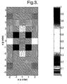
- the magnitudes of the diffraction orders of this mask feature are plotted in Figure 3.
- the largest order is the (0,0) order or the DC background light.
- the orders that contribute the most to imaging are the ( ⁇ 2,0) orders and represent the vertical bricks in the brick wall pattern.
- the other significant order is the ( ⁇ 1, ⁇ 1) which represents the clear areas and defines the end of the isolation pattern.
- the higher orders also help to define two dimensional structures such as the end of each line. Since the diffraction orders are not constant, the orders change the weighting coefficients in the DOCC, which implies that the mask pattern influences the illumination strategy.
- the diffraction order coefficients T(m,n) in Figure 3 can be substituted into Equation 13 to calculate J opt-2D and are plotted in Figure 4.
- the (0,0) order does not contribute to imaging and decreases the DOF.
- this (0,0) order can be subtracted from the total illumination, J tot .
- the DOCC approach shows how the illumination pupil is sampled for improved image formation and is an effective method for understanding imaging of the brick wall isolation pattern.
- the illumination pupil of the brick wall pattern for the 130nm design rule can be calculated and is shown in Figure 5.
- Figure 5 shows that the most significant areas for image formation are the outer portions of the illumination configuration along the x-axis. These outer portions form an elliptical dipole. In addition to these elliptical dipole elements, the center of the illumination pupil has a large contribution to image formulation.
- the illumination pupil can be implemented in gray scale or binary illumination profiles.
- gray scale illumination may be possible.
- controllable illumination intensity for which a normalized level ranging from 0 to 1 may be selected for at least given portions of the illumination configuration.
- control over illumination intensity may be produced by use of a diffractive optical element (DOE) in the illumination system.
- DOE diffractive optical element
- the illumination configuration can be implemented as shown in Figure 5.
- some of the local spikes which are calculated in theory and seen in Figure 5 will be removed after low pass filtering of the illumination information as a result of the projection optics, as discussed above. Therefore, when designing an illumination configuration, spikes which will be filtered should be ignored.
- a threshold value should be chosen as a basis for assigning values of 0 or 1 to each point on the illumination configuration. For example, if a threshold of 0.8 is chosen, illuminator intensity values above 0.8 are rounded up to 1 and values below 0.8 are rounded down to 0. Other threshold values may be applied as desired.
- Example 2 Using the gray scale to binary approach, a binary illumination configuration for the same brick wall isolation pattern was designed assuming a maximum outer ⁇ of 0.88 and is shown in Figure 6.
- the vector (thin-film) imaging resist model was used since the numerical aperture was above 0.7.
- This annular setting has approximately 0.4 ⁇ m of DOF from -0.4 ⁇ m to 0.0 ⁇ m focus.
- the contrast of the resist is low through focus, and can be imaged with a low contrast resist.
- MEEF mask error enhancement factor
- EL exposure latitude
- the top down images in Figure 7 also show that there is approximately 20nm of end of line (EOL) shortening, which can be fixed by extending the line slightly for the 130nm design rule.
- EOL end of line
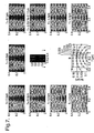
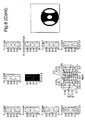
- simulation results for the 130nm design rule brick wall isolation pattern are plotted for a binary mask feature with NA of 0.8 and using the optimized binary illumination configuration in FIG. 6.
- the optimal illumination configuration has approximately 0.6 ⁇ m DOF from -0.45 ⁇ m to +0.15 ⁇ m focus.
- the optimized illumination configuration has a larger contrast through focus as compared to annular illumination. This larger contrast implies that the MEEF for the optimized illumination configuration is lower compared to annular illumination and that the exposure latitude for the optimized illumination configuration is higher.
- Another benefit of the optimized illumination configuration is the improved line end performance as compared to annular illumination.
- the top down images in Figure 8 show that the optimized illumination configuration is capable of maintaining the EOL without extending the line on the pattern, which is advantageous for more aggressive design rule shrinks.
- Example 3 The results in Figures 7 and 8 for binary mask (BIM) were compared to simulation results for chromeless mask (CLM).
- a chromeless brick wall isolation pattern was designed from experimental results of software simulation in a manner known to those skilled in the art.
- the chromeless technology requires (0,0) order light so as to fully benefit from the DOF improvement produced by off axis illumination.
- Experimental results from the simulation confirm the need for (0,0) order light for which purpose the isolation layer should be dithered or half toned.
- the half tone pitch may be chosen such that the first order in the dithered direction does not fall into the projection pupil.
- the lines were dithered in the vertical direction with pitch less than ⁇ /[NA(1+ ⁇ out )].
- the dithering duty cycle should be tuned to optimize the amount of (0,0) order light for best DOF and pattern fidelity.
- the half tone pitch was 155nm with 50% duty cycle (77.5nm chrome islands). This pitch substantially prevented the (0, ⁇ 1) orders from entering the projection pupil; however, this duty cycle should be tuned to maximum DOF with computer aided design tools.
- Example 4 Simulation results for the 130nm design rule layer were plotted for a CLM with 155nm halftone pitch and 50% duty cycle.
- the CLM with this annular setting had 0.5 ⁇ m DOF (-0.4 ⁇ m focus to +0.1 ⁇ m focus).
- the CLM with annular illumination had greater DOF and better contrast through focus as compared to BIM with annular illumination. This indicates that the CLM performed better than the BIM mask.
- the top down simulation results indicated that the EOL performance with CLM is theoretically better than the EOL performance with BIM and that the CLM was also able to better define the contact hole landing area as compared to BIM.
- the linewidth may be corrected, for example, by biasing and by modifying the half tone duty cycle.
- the top down simulation results indicated that CLM was able to define the contact landing region and was able to maintain CD uniformity. Necking and other linewidth inconsistencies were reduced with this elliptical illumination configuration. Furthermore, the CLM reticle could be biased to improve the DOF, and consequently the EOL performance should improve. Furthermore, model based OPC should be able to correct the EOL further.
- Example 6 Using the mask pattern of Figure 2 for a 110nm design rule isolation layer, an optimized illumination configuration was generated with Equations 13 and 15.
- Figure 9 also shows that the ( ⁇ 1, ⁇ 1) orders are the largest contributors to the illumination configuration optimization rather than the ( ⁇ 2,0) order.
- the orders that contribute most to defining the isolation linewidth are the ( ⁇ 2,0) orders.
- the ( ⁇ 2,0) orders are at the far edge of the illumination configuration (0.8 ⁇ a ⁇ 1.0), which indicates that ⁇ of 1 may provide improvement to implement the 110nm design rule at this wavelength.
- the optimized illumination configuration for the 110nm brick wall isolation layer is shown in Figure 10.
- Figure 10 shows that the illumination configuration areas that contribute most to image formation are a small portion in the center and far edges of the illumination configuration.
- One possible implementation of this illumination configuration is plotted in Figure 11a.
- an illumination configuration with ⁇ of 1.0, as shown in Figure 11b, and with small sectors ( ⁇ ring width of 0.2) may be used.
- An implementation of the present invention includes selection of cells or particular gates that are critical. These critical features are then processed to determine J tot as described above.
- Section 1 it was shown that the illumination configuration is pattern dependent. Therefore, if the pitch does not differ significantly for the critical features, it is possible to create a single illumination configuration which optimizes the process window for all the critical features.
- Figure 12 an example of a circuit with critical gates g 1 , g 2 , g 3 and a critical cell cc is shown. The diffraction orders of these tagged critical features can be calculated, and by using the theory already described, the optimized illumination configuration can be calculated. After calculating the optimized illumination configuration the process window can be calculated and compared to the process window with other illumination configurations.
- Another method of optimizing illumination/pattern interaction is to modify the pattern design with scattering bars.
- Scattering bars discretize the pitch from a semi-continuous function for an ASIC or logic design. After placing scattering bars, there are fewer pitches. This can be demonstrated in simulation software by placing the scattering bars with an edge-to-edge separation of 0.61 ⁇ /NA.
- the design in Figure 12 has been modified by adding a plurality of scattering bars.
- the illumination configuration can then be optimized for the modified design.
- the process window performance of an illumination configuration optimized for a design with scattering bars can then be compared to the process window of an illumination configuration optimized without scattering bars. Since a design with scattering bars discretizes the pitch, the combination of scattering bars with optimized off axis illumination (OAI) will have the largest possible DOF process window.
- OAI off axis illumination
- Another concept for implementing illumination configuration optimization is through the placing of scattering bars based on space width (SW) considerations.
- a scattering bar is placed through rule based OPC which rules may be defined by the space width.
- PDF probability density function
- the illumination can than be optimized by considering the pdf by modifying J opt-2D as shown in Equation 16. Assuming that the vertical lines and horizontal lines are infinite, it is also possible to calculate the diffraction orders T(m,n).
- T ( m , n ) ⁇ 1 - w ( 1 + ⁇ ) ( 1 P x + 1 P y ) + w 2 P x P y ( 1 + ⁇ ) 2 [ 1 - w P x ( 1 + ⁇ ) ] ( 1 + ⁇ ) ( P y ⁇ n ) sin ( n ⁇ w P y ) [ 1 - w P y ( 1 + ⁇ ) ] ( 1 + ⁇ ) ( P x ⁇ m ) sin ( m ⁇ w P x ) ( 1 + ⁇ ) 2 ( P x ⁇ m ) sin ( m ⁇ w P x ) ( P y ⁇ n ) sin ( n
- FIG 14 is an example pdf for a logic pattern with features oriented in the y-direction (i.e. "vertical" direction) in which scattering bars have and have not been applied.
- Figure 14 shows vertical gate space widths ( ⁇ m) on the x (horizontal) axis.
- D without scattering bars
- D+SB the number of pitches has been reduced such that most of the space widths are at dense pitches of 0.2 ⁇ m. With this change to the pdf, it is more likely that an illumination configuration can be optimized.
- the total illumination configuration for a design with both horizontal (x-direction) and vertical features is the sum of horizontal and vertical illumination configurations. If the illumination configuration is concentrated at ⁇ cx for the vertical features and is concentrated at ⁇ cy for the horizontal features, the optimal illumination configuration will be a "conventional" quadrupole illumination configuration provided that 2 ⁇ cx ⁇ 1 and that 2 ⁇ cy ⁇ 1 . Otherwise, this type of analysis will result in a four pole illumination configuration that has been rotated 45°
- the illumination technique presented herein may be extended to account for aberrations. Including aberrations allows an operator to determine which part of the illumination configuration couples to the aberration. The amount of coupling is directly related to sensitivity of the image intensity to the aberration. By understanding this coupling, it may be possible to modify the illumination configuration to minimize the aberration sensitivity of a design.
- the projection pupil, K( ⁇ , ⁇ ), for scalar imaging contains the obliquity factor, defocus, and the exponential of the wavefront represented by the Zernike polynomials.
- This scalar imaging pupil is shown in Equation 18.
- This pupil can further be divided into two parts, the unaberrated pupil K 0 ( ⁇ , ⁇ ) and the aberrated pupil (the exponential of the wavefront); these two parts are multiplied together as shown in Equation 19.
- Equation 23 the wavefront can be written as a linear approximation, which is shown in Equation 23.
- Equation 23 the linear approximation for the projection pupil, K( ⁇ , ⁇ )
- Equation 24 Since the TCC is a function of the projection pupil, K( ⁇ , ⁇ ), the linear approximation to the pupil in Equation 24 implies that the TCC can be represented by a linear approximation. This is accomplished by substituting Equation 24 into Equation 1, which results in Equation 25. Once again by neglecting the terms of power 2 or greater, the TCC in Equation 25 can be simplified as shown in Equation 26.
- Equation 21 The wavefront, W( ⁇ , ⁇ ), is most often denoted by the summation of Zernike fringe polynomials as shown in Equation 21.
- the exponential, e x can be represented by a Taylor series expansion.
- the Taylor series expansion is valid for small x, and previous work has shown good agreement for aerial images when Z v is less than 0.04 ⁇ .
- the TCC can be represented by a linear function of TCC 0 and TCC v as shown in Equation 29.
- Equation 30 The linear approximation to J opt is derived in Equation 30 by using Equation 8 for J opt and by following the methodology for the linear approximation of the TCC as outlined in Equations 18 through 29.
- Equation 30 for J opt can then be divided into a summation of the unaberrated J opt0 with the aberrated J opt v as shown in Equation 33.
- the definition of J opt0 and J opt v are shown in Equations 31 and 32, respectively.
- J opt ( ⁇ , ⁇ , m , n , p , q ) J s ( ⁇ , ⁇ ) K 0 ( ⁇ + m ⁇ P x NA , ⁇ + n ⁇ P y NA ) K 0 * ( ⁇ - p ⁇ P x NA , ⁇ - q ⁇ P y NA )
- J opt ( ⁇ , ⁇ , m , n , p , q ) - i 2 ⁇ ⁇ J s ( ⁇ , ⁇ ) K 0 ( ⁇ + m ⁇ P x NA , ⁇ + n ⁇ P y NA ) ⁇ K 0 *
- Equation 32 describes the portion of the illumination configuration which couples to a particular aberration. The amount of coupling affects the image intensity and helps to provide an understanding of aberration sensitivity to illumination.
- J opt can be written as a linear approximation.
- weighting factors can be introduced to maximize or to minimize a response to a particular metric including, for example, depth of focus (DOF), image log slope (ILS), image slope (IS), or aberration sensitivity.
- the optimal J tot of Equation 15 can be modified to include these weighting factors as shown in Equation 34.
- J tot ( ⁇ , ⁇ ) ⁇ m ⁇ n ⁇ p ⁇ w w ( ⁇ , ⁇ , m , n , p , q ) J opt ( ⁇ , ⁇ , m , n , p , q )
- ILS logarithmic change in intensity
- Equation 35 Since the derivative of the intensity changes faster than the inverse of intensity, Equation 35 will increase more by increasing the derivative of the intensity.
- the intensity can be calculated from Equation 3 and the derivative of the intensity with respect to x is defined in Equation 36.
- the derivative with respect to x results in the weighting function, w x , as shown in Equation 37.
- a weighting function w y can be defined with respect to y as shown in Equation 38.
- Equation 39 This allows us to define a weighting function to calculate J tot in Equation 34.
- 2 w ILS ( m , n , p , q ) 2 ⁇ ( m + p P x ) 2 + ( n + q P y ) 2
- Equation 41 The pupil, K( ⁇ , ⁇ ), is shown in Equation 41, where focus is denoted z. Equation 41 can be divided into two terms, terms dependant on z (the defocus term) and terms independent of z (the non-defocus term), as shown in Equation 42.
- Equation 43 K d ( ⁇ + m ⁇ P x NA , ⁇ + n ⁇ P y NA ) K d * ( ⁇ - p ⁇ P x NA , ⁇ - q ⁇ P y NA )
- Equation 44 The cost function, f( ⁇ , ⁇ ,z), is in turn minimized when g( ⁇ , ⁇ ,m,n,p,q) equals zero (see Equation 44, below).
- Equation 44 the phase terms have been removed as the derivative with respect to z equals zero only when the magnitude terms equal zero.
- g( ⁇ , ⁇ ,m,n,p,q) is zero, the areas ( ⁇ , ⁇ ) of the pupil for a given order (m,n,p,q) are minimally sensitive to focus. These are the most desired areas of the pupil for constructing the illumination configuration.
- a weighting function, w focus ( ⁇ , ⁇ ,m,n,p,q) is defined in Equation 45.
- This weighting function is equal to 1 for areas least sensitive to focus and is equal 0 for areas most sensitive to focus.
- a new weighting function which maximizes ILS through focus can then be defined by Equation 46 and used to modify the illumination configuration.
- w focus ( ⁇ , ⁇ , m , n , p , q ) 1 -
- the above methodology allows the sensitivity of the intensity to be minimized to the influence of focus, an aberration. Since the impact of focus on intensity can be minimized, the impact of intensity can be minimized to a specific aberration. This is desirable for certain patterns which demonstrate a high sensitivity to a particular aberration.
- the projection pupil in Equation 19 can be written as an unaberrated term, K 0 ( ⁇ , ⁇ ), multiplied by an aberrated term, K a ( ⁇ , ⁇ ) as shown in Equation 47.
- K ( ⁇ , ⁇ ) K 0 ( ⁇ , ⁇ ) K a ( ⁇ , ⁇ )
- the sensitivity of the intensity to a particular aberration Z i can be minimized by setting the derivative of the intensity with respect to Z i to zero.
- the aberration sensitivity is minimized when h( ⁇ , ⁇ ,m,n,p,q) in Equation 48 is equal to zero.
- Equation 48 may be simplified and written as Equation 49.
- a weighting function w ab ( ⁇ , ⁇ ,m,n,p,q) is defined in Equation 50, which equates to 1 for areas ( ⁇ , ⁇ ) of the pupil that are least sensitive to Z i and to 0 for areas most sensitive to Z i .
- w ab ( ⁇ , ⁇ , m , n , p , q ) 1 - 1 2
- Equation 51 The weighting function to minimize ILS sensitivity to a particular aberration, Z i , can then be defined in Equation 51.
- a weighting function to minimize ILS sensitivity to a particular aberration, Z i , and to maximize ILS through focus can also be defined in Equation 52. Either of these equations can be substituted into Equation 34 to calculate the illuminator with the optimal response to a given metric.
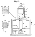
- FIG 15 is a schematic representation of an example of a lithography apparatus for use according to the present invention.
- the apparatus includes a radiation system.
- the radiation system is made up of a lamp LA (which may be an excimer laser, for example) and an illumination system which may comprise beam shaping optics EX, an integrator IN, and a condenser lens CO, for example.
- the radiation system supplies a projection beam PB of radiation.
- the radiation system may provide ultraviolet, deep ultraviolet or extreme ultraviolet radiation. In general, the radiation system may also provide soft x-ray or other forms of radiation.
- a first object table, or mask table MT holds a mask MA.
- the mask MA includes a pattern area C which contains the mask pattern to be imaged.
- the mask table MT is movable relative to the projection beam PB so that different portions of the mask may be irradiated.
- Alignment marks M 1 and M 2 are used for determining whether the mask is properly aligned with the substrate, or wafer, W.
- a projection system PL projects the projection beam PB onto the wafer W.
- the wafer W includes two alignment marks P 1 and P 2 which are aligned with the marks M 1 and M 2 prior to beginning imaging.
- the wafer W is supported by a substrate table WT which is moveable relative to the projection beam for exposing different parts of the wafer W; in this way, the mask pattern C may be imaged onto different target portions c of the wafer W.
- An interferometric position monitor IF is used to insure that the wafer table WT is in the correct position relative to the position of the mask table MT.
Landscapes
- Physics & Mathematics (AREA)
- General Physics & Mathematics (AREA)
- Exposure And Positioning Against Photoresist Photosensitive Materials (AREA)
Applications Claiming Priority (2)
| Application Number | Priority Date | Filing Date | Title |
|---|---|---|---|
| US27130501P | 2001-02-23 | 2001-02-23 | |
| EP02251203A EP1239331B1 (de) | 2001-02-23 | 2002-02-22 | Beleuchtungsoptimierung für spezifische Maskenmuster |
Related Parent Applications (1)
| Application Number | Title | Priority Date | Filing Date |
|---|---|---|---|
| EP02251203A Division EP1239331B1 (de) | 2001-02-23 | 2002-02-22 | Beleuchtungsoptimierung für spezifische Maskenmuster |
Publications (2)
| Publication Number | Publication Date |
|---|---|
| EP1612606A2 true EP1612606A2 (de) | 2006-01-04 |
| EP1612606A3 EP1612606A3 (de) | 2009-03-25 |
Family
ID=35464038
Family Applications (1)
| Application Number | Title | Priority Date | Filing Date |
|---|---|---|---|
| EP05021788A Withdrawn EP1612606A3 (de) | 2001-02-23 | 2002-02-22 | Beleuchtungsoptimierung für spezifische Maskenmuster |
Country Status (1)
| Country | Link |
|---|---|
| EP (1) | EP1612606A3 (de) |
Cited By (1)
| Publication number | Priority date | Publication date | Assignee | Title |
|---|---|---|---|---|
| CN108931883A (zh) * | 2017-05-17 | 2018-12-04 | 东方晶源微电子科技(北京)有限公司 | 一种优化掩模版图的方法 |
Family Cites Families (3)
| Publication number | Priority date | Publication date | Assignee | Title |
|---|---|---|---|---|
| KR960002536A (de) * | 1994-06-29 | 1996-01-26 | ||
| JP2910716B2 (ja) * | 1997-01-16 | 1999-06-23 | 日本電気株式会社 | 光強度計算のパラメトリック解析方法 |
| US5821014A (en) * | 1997-02-28 | 1998-10-13 | Microunity Systems Engineering, Inc. | Optical proximity correction method for intermediate-pitch features using sub-resolution scattering bars on a mask |
-
2002
- 2002-02-22 EP EP05021788A patent/EP1612606A3/de not_active Withdrawn
Cited By (2)
| Publication number | Priority date | Publication date | Assignee | Title |
|---|---|---|---|---|
| CN108931883A (zh) * | 2017-05-17 | 2018-12-04 | 东方晶源微电子科技(北京)有限公司 | 一种优化掩模版图的方法 |
| CN108931883B (zh) * | 2017-05-17 | 2022-06-21 | 东方晶源微电子科技(北京)有限公司 | 一种优化掩模版图的方法 |
Also Published As
| Publication number | Publication date |
|---|---|
| EP1612606A3 (de) | 2009-03-25 |
Similar Documents
| Publication | Publication Date | Title |
|---|---|---|
| EP1239331B1 (de) | Beleuchtungsoptimierung für spezifische Maskenmuster | |
| CN102224459B (zh) | 用于优化光刻过程的方法及设备 | |
| KR100839972B1 (ko) | 리소그래피 장치 및 디바이스 제조 방법 | |
| KR100457839B1 (ko) | 규정된 래더바를 서브-해상도 어시스트피처로 활용하는광근접성교정방법 | |
| KR100617909B1 (ko) | 리소그래피장치 및 포토리소그래피 시뮬레이션을 이용하여조명소스를 최적화시키는 방법 | |
| EP1237046B1 (de) | Verfahren zur identifizierung von Regionen extremer Wechselwirkung, Verfahren zum Entwerfen von Maskenmustern und zur Herstellung von Masken, Verfahren zur Herstellung von Elementen und Computerprogramme | |
| JP3992688B2 (ja) | コンタクト・ホール・マスクの光学的近接補正設計の方法 | |
| US7506299B2 (en) | Feature optimization using interference mapping lithography | |
| US10657641B2 (en) | Source and mask optimization by changing intensity and shape of the illumination source and magnitude and phase of mask diffraction orders | |
| EP1630614B1 (de) | Verfahren zum Entwurf einer Beleuchtungsquelle, Verfahren zum Entwurf einer Maskenstruktur, Verfahren zur Herstellung einer Photomaske, Verfahren zur Herstellung eines Halbleiterbauelements und Computerprogrammprodukt | |
| CN100576066C (zh) | 优化图案强度轮廓的方法 | |
| EP1513012B1 (de) | Methode und Vorrichtung für modellgestützte Plazierung phasenbalancierter Hilfsstrukturen für optische Lithographie mit Auflösungsgrenzen unterhalb der Belichtungswellenlänge | |
| EP1530083A2 (de) | Korrektur optischer Naheffekte basiert auf Zerlegung in Eigenfunktionen | |
| US20040142251A1 (en) | Method and apparatus for performing model-based layout conversion for use with dipole illumination | |
| JP4056462B2 (ja) | リソグラフィ投影用パラメータを決める方法、そのためのコンピュータシステムおよびコンピュータプログラム、デバイス製造方法並びにそれによって製造したデバイス | |
| JP2004133426A (ja) | 自動光近接補正(opc)ルール作成 | |
| EP1544680A2 (de) | Maskenstrukturoptimierung mittels lithographischer Interferenzabbildung | |
| US20050136340A1 (en) | Lithographic apparatus and methods, patterning structure and method for making a patterning structure, device manufacturing method, and device manufactured thereby | |
| EP1420301A2 (de) | Kompensation von Linsenaberrationen durch Beleuchtungsoptimierung | |
| US8043797B2 (en) | Lithographic apparatus and device manufacturing method | |
| EP1248154A1 (de) | Lithographisches Herstellungsverfahren und lithographischer Projektionsapparat | |
| EP1429191B1 (de) | Verfahren zur Parameterbestimmung für lithographische Projektion |
Legal Events
| Date | Code | Title | Description |
|---|---|---|---|
| PUAI | Public reference made under article 153(3) epc to a published international application that has entered the european phase |
Free format text: ORIGINAL CODE: 0009012 |
|
| AC | Divisional application: reference to earlier application |
Ref document number: 1239331 Country of ref document: EP Kind code of ref document: P |
|
| AK | Designated contracting states |
Kind code of ref document: A2 Designated state(s): DE FR GB IT NL |
|
| PUAL | Search report despatched |
Free format text: ORIGINAL CODE: 0009013 |
|
| AK | Designated contracting states |
Kind code of ref document: A3 Designated state(s): DE FR GB IT NL |
|
| AKX | Designation fees paid | ||
| REG | Reference to a national code |
Ref country code: DE Ref legal event code: 8566 |
|
| STAA | Information on the status of an ep patent application or granted ep patent |
Free format text: STATUS: THE APPLICATION IS DEEMED TO BE WITHDRAWN |
|
| 18D | Application deemed to be withdrawn |
Effective date: 20090901 |