EP1614765A2 - Niedertemperaturwachstum orientierter Kohlenstoff-Nanoröhrchen - Google Patents
Niedertemperaturwachstum orientierter Kohlenstoff-Nanoröhrchen Download PDFInfo
- Publication number
- EP1614765A2 EP1614765A2 EP05106104A EP05106104A EP1614765A2 EP 1614765 A2 EP1614765 A2 EP 1614765A2 EP 05106104 A EP05106104 A EP 05106104A EP 05106104 A EP05106104 A EP 05106104A EP 1614765 A2 EP1614765 A2 EP 1614765A2
- Authority
- EP
- European Patent Office
- Prior art keywords
- sample
- process according
- plasma
- carbon
- carbon nanotubes
- Prior art date
- Legal status (The legal status is an assumption and is not a legal conclusion. Google has not performed a legal analysis and makes no representation as to the accuracy of the status listed.)
- Granted
Links
- OKTJSMMVPCPJKN-UHFFFAOYSA-N Carbon Chemical compound [C] OKTJSMMVPCPJKN-UHFFFAOYSA-N 0.000 title claims abstract description 53
- 229910021393 carbon nanotube Inorganic materials 0.000 title claims abstract description 29
- 239000002041 carbon nanotube Substances 0.000 title claims abstract description 28
- 238000000034 method Methods 0.000 claims abstract description 29
- UFHFLCQGNIYNRP-UHFFFAOYSA-N Hydrogen Chemical compound [H][H] UFHFLCQGNIYNRP-UHFFFAOYSA-N 0.000 claims abstract description 16
- 229910052799 carbon Inorganic materials 0.000 claims abstract description 16
- 239000007789 gas Substances 0.000 claims abstract description 16
- 239000001257 hydrogen Substances 0.000 claims abstract description 16
- 229910052739 hydrogen Inorganic materials 0.000 claims abstract description 16
- XKRFYHLGVUSROY-UHFFFAOYSA-N Argon Chemical compound [Ar] XKRFYHLGVUSROY-UHFFFAOYSA-N 0.000 claims abstract description 12
- QGZKDVFQNNGYKY-UHFFFAOYSA-N Ammonia Chemical compound N QGZKDVFQNNGYKY-UHFFFAOYSA-N 0.000 claims abstract description 8
- IJGRMHOSHXDMSA-UHFFFAOYSA-N Atomic nitrogen Chemical compound N#N IJGRMHOSHXDMSA-UHFFFAOYSA-N 0.000 claims abstract description 8
- 229910052786 argon Inorganic materials 0.000 claims abstract description 6
- HSFWRNGVRCDJHI-UHFFFAOYSA-N alpha-acetylene Natural products C#C HSFWRNGVRCDJHI-UHFFFAOYSA-N 0.000 claims abstract description 5
- 125000002534 ethynyl group Chemical group [H]C#C* 0.000 claims abstract description 5
- 229910052743 krypton Inorganic materials 0.000 claims abstract description 5
- DNNSSWSSYDEUBZ-UHFFFAOYSA-N krypton atom Chemical compound [Kr] DNNSSWSSYDEUBZ-UHFFFAOYSA-N 0.000 claims abstract description 5
- 229910052724 xenon Inorganic materials 0.000 claims abstract description 5
- FHNFHKCVQCLJFQ-UHFFFAOYSA-N xenon atom Chemical compound [Xe] FHNFHKCVQCLJFQ-UHFFFAOYSA-N 0.000 claims abstract description 5
- 229910021529 ammonia Inorganic materials 0.000 claims abstract description 4
- 229910052757 nitrogen Inorganic materials 0.000 claims abstract description 4
- 230000008021 deposition Effects 0.000 claims description 10
- 239000000758 substrate Substances 0.000 claims description 9
- 239000008246 gaseous mixture Substances 0.000 claims description 7
- 239000000463 material Substances 0.000 claims description 5
- 230000003197 catalytic effect Effects 0.000 claims description 3
- 239000011521 glass Substances 0.000 claims description 2
- 239000004065 semiconductor Substances 0.000 claims description 2
- 239000002071 nanotube Substances 0.000 abstract description 15
- 239000000203 mixture Substances 0.000 abstract description 3
- UGFAIRIUMAVXCW-UHFFFAOYSA-N Carbon monoxide Chemical compound [O+]#[C-] UGFAIRIUMAVXCW-UHFFFAOYSA-N 0.000 abstract description 2
- 229910002091 carbon monoxide Inorganic materials 0.000 abstract description 2
- CURLTUGMZLYLDI-UHFFFAOYSA-N Carbon dioxide Chemical compound O=C=O CURLTUGMZLYLDI-UHFFFAOYSA-N 0.000 abstract 1
- 230000000977 initiatory effect Effects 0.000 abstract 1
- 238000000151 deposition Methods 0.000 description 9
- PXHVJJICTQNCMI-UHFFFAOYSA-N Nickel Chemical compound [Ni] PXHVJJICTQNCMI-UHFFFAOYSA-N 0.000 description 8
- 229910002804 graphite Inorganic materials 0.000 description 7
- 239000010439 graphite Substances 0.000 description 7
- ATJFFYVFTNAWJD-UHFFFAOYSA-N Tin Chemical compound [Sn] ATJFFYVFTNAWJD-UHFFFAOYSA-N 0.000 description 5
- 239000003054 catalyst Substances 0.000 description 4
- 238000006243 chemical reaction Methods 0.000 description 4
- 229910052759 nickel Inorganic materials 0.000 description 4
- 238000004626 scanning electron microscopy Methods 0.000 description 4
- 238000003786 synthesis reaction Methods 0.000 description 4
- XUIMIQQOPSSXEZ-UHFFFAOYSA-N Silicon Chemical compound [Si] XUIMIQQOPSSXEZ-UHFFFAOYSA-N 0.000 description 3
- 239000003990 capacitor Substances 0.000 description 3
- 229910052710 silicon Inorganic materials 0.000 description 3
- 239000010703 silicon Substances 0.000 description 3
- XMWRBQBLMFGWIX-UHFFFAOYSA-N C60 fullerene Chemical class C12=C3C(C4=C56)=C7C8=C5C5=C9C%10=C6C6=C4C1=C1C4=C6C6=C%10C%10=C9C9=C%11C5=C8C5=C8C7=C3C3=C7C2=C1C1=C2C4=C6C4=C%10C6=C9C9=C%11C5=C5C8=C3C3=C7C1=C1C2=C4C6=C2C9=C5C3=C12 XMWRBQBLMFGWIX-UHFFFAOYSA-N 0.000 description 2
- XEEYBQQBJWHFJM-UHFFFAOYSA-N Iron Chemical compound [Fe] XEEYBQQBJWHFJM-UHFFFAOYSA-N 0.000 description 2
- 102000029749 Microtubule Human genes 0.000 description 2
- 108091022875 Microtubule Proteins 0.000 description 2
- ZOKXTWBITQBERF-UHFFFAOYSA-N Molybdenum Chemical compound [Mo] ZOKXTWBITQBERF-UHFFFAOYSA-N 0.000 description 2
- RTAQQCXQSZGOHL-UHFFFAOYSA-N Titanium Chemical compound [Ti] RTAQQCXQSZGOHL-UHFFFAOYSA-N 0.000 description 2
- 239000002134 carbon nanofiber Substances 0.000 description 2
- 239000004020 conductor Substances 0.000 description 2
- 238000005520 cutting process Methods 0.000 description 2
- 238000010586 diagram Methods 0.000 description 2
- 229910003472 fullerene Inorganic materials 0.000 description 2
- 238000010438 heat treatment Methods 0.000 description 2
- 210000004688 microtubule Anatomy 0.000 description 2
- 229910052750 molybdenum Inorganic materials 0.000 description 2
- 239000011733 molybdenum Substances 0.000 description 2
- 238000000623 plasma-assisted chemical vapour deposition Methods 0.000 description 2
- BASFCYQUMIYNBI-UHFFFAOYSA-N platinum Chemical compound [Pt] BASFCYQUMIYNBI-UHFFFAOYSA-N 0.000 description 2
- 239000002296 pyrolytic carbon Substances 0.000 description 2
- 238000001552 radio frequency sputter deposition Methods 0.000 description 2
- 238000001338 self-assembly Methods 0.000 description 2
- VYPSYNLAJGMNEJ-UHFFFAOYSA-N silicon dioxide Inorganic materials O=[Si]=O VYPSYNLAJGMNEJ-UHFFFAOYSA-N 0.000 description 2
- 241000894007 species Species 0.000 description 2
- 239000010936 titanium Substances 0.000 description 2
- 229910052719 titanium Inorganic materials 0.000 description 2
- 235000017166 Bambusa arundinacea Nutrition 0.000 description 1
- 235000017491 Bambusa tulda Nutrition 0.000 description 1
- 241001330002 Bambuseae Species 0.000 description 1
- 239000004215 Carbon black (E152) Substances 0.000 description 1
- 235000015334 Phyllostachys viridis Nutrition 0.000 description 1
- 229910021417 amorphous silicon Inorganic materials 0.000 description 1
- 239000011425 bamboo Substances 0.000 description 1
- 239000005388 borosilicate glass Substances 0.000 description 1
- 239000013590 bulk material Substances 0.000 description 1
- 238000007036 catalytic synthesis reaction Methods 0.000 description 1
- 239000010941 cobalt Substances 0.000 description 1
- 229910017052 cobalt Inorganic materials 0.000 description 1
- GUTLYIVDDKVIGB-UHFFFAOYSA-N cobalt atom Chemical compound [Co] GUTLYIVDDKVIGB-UHFFFAOYSA-N 0.000 description 1
- 238000005336 cracking Methods 0.000 description 1
- 239000013078 crystal Substances 0.000 description 1
- 238000005530 etching Methods 0.000 description 1
- 238000000605 extraction Methods 0.000 description 1
- 229930195733 hydrocarbon Natural products 0.000 description 1
- 150000002430 hydrocarbons Chemical class 0.000 description 1
- 238000009413 insulation Methods 0.000 description 1
- 238000010849 ion bombardment Methods 0.000 description 1
- 229910052742 iron Inorganic materials 0.000 description 1
- 238000001755 magnetron sputter deposition Methods 0.000 description 1
- 238000004519 manufacturing process Methods 0.000 description 1
- 230000003071 parasitic effect Effects 0.000 description 1
- 239000008188 pellet Substances 0.000 description 1
- 238000000206 photolithography Methods 0.000 description 1
- 229910052697 platinum Inorganic materials 0.000 description 1
- 239000010453 quartz Substances 0.000 description 1
- 229910052814 silicon oxide Inorganic materials 0.000 description 1
- 239000007787 solid Substances 0.000 description 1
- 238000005507 spraying Methods 0.000 description 1
- 238000004544 sputter deposition Methods 0.000 description 1
- 239000013077 target material Substances 0.000 description 1
- 238000002230 thermal chemical vapour deposition Methods 0.000 description 1
Images

Classifications
-
- B—PERFORMING OPERATIONS; TRANSPORTING
- B82—NANOTECHNOLOGY
- B82Y—SPECIFIC USES OR APPLICATIONS OF NANOSTRUCTURES; MEASUREMENT OR ANALYSIS OF NANOSTRUCTURES; MANUFACTURE OR TREATMENT OF NANOSTRUCTURES
- B82Y40/00—Manufacture or treatment of nanostructures
-
- B—PERFORMING OPERATIONS; TRANSPORTING
- B82—NANOTECHNOLOGY
- B82Y—SPECIFIC USES OR APPLICATIONS OF NANOSTRUCTURES; MEASUREMENT OR ANALYSIS OF NANOSTRUCTURES; MANUFACTURE OR TREATMENT OF NANOSTRUCTURES
- B82Y30/00—Nanotechnology for materials or surface science, e.g. nanocomposites
-
- C—CHEMISTRY; METALLURGY
- C01—INORGANIC CHEMISTRY
- C01B—NON-METALLIC ELEMENTS; COMPOUNDS THEREOF; METALLOIDS OR COMPOUNDS THEREOF NOT COVERED BY SUBCLASS C01C
- C01B32/00—Carbon; Compounds thereof
- C01B32/15—Nano-sized carbon materials
- C01B32/158—Carbon nanotubes
- C01B32/16—Preparation
- C01B32/162—Preparation characterised by catalysts
-
- C—CHEMISTRY; METALLURGY
- C03—GLASS; MINERAL OR SLAG WOOL
- C03C—CHEMICAL COMPOSITION OF GLASSES, GLAZES OR VITREOUS ENAMELS; SURFACE TREATMENT OF GLASS; SURFACE TREATMENT OF FIBRES OR FILAMENTS MADE FROM GLASS, MINERALS OR SLAGS; JOINING GLASS TO GLASS OR OTHER MATERIALS
- C03C17/00—Surface treatment of glass, not in the form of fibres or filaments, by coating
- C03C17/34—Surface treatment of glass, not in the form of fibres or filaments, by coating with at least two coatings having different compositions
- C03C17/36—Surface treatment of glass, not in the form of fibres or filaments, by coating with at least two coatings having different compositions at least one coating being a metal
-
- C—CHEMISTRY; METALLURGY
- C03—GLASS; MINERAL OR SLAG WOOL
- C03C—CHEMICAL COMPOSITION OF GLASSES, GLAZES OR VITREOUS ENAMELS; SURFACE TREATMENT OF GLASS; SURFACE TREATMENT OF FIBRES OR FILAMENTS MADE FROM GLASS, MINERALS OR SLAGS; JOINING GLASS TO GLASS OR OTHER MATERIALS
- C03C17/00—Surface treatment of glass, not in the form of fibres or filaments, by coating
- C03C17/34—Surface treatment of glass, not in the form of fibres or filaments, by coating with at least two coatings having different compositions
- C03C17/36—Surface treatment of glass, not in the form of fibres or filaments, by coating with at least two coatings having different compositions at least one coating being a metal
- C03C17/3602—Surface treatment of glass, not in the form of fibres or filaments, by coating with at least two coatings having different compositions at least one coating being a metal the metal being present as a layer
- C03C17/3615—Coatings of the type glass/metal/other inorganic layers, at least one layer being non-metallic
-
- C—CHEMISTRY; METALLURGY
- C03—GLASS; MINERAL OR SLAG WOOL
- C03C—CHEMICAL COMPOSITION OF GLASSES, GLAZES OR VITREOUS ENAMELS; SURFACE TREATMENT OF GLASS; SURFACE TREATMENT OF FIBRES OR FILAMENTS MADE FROM GLASS, MINERALS OR SLAGS; JOINING GLASS TO GLASS OR OTHER MATERIALS
- C03C17/00—Surface treatment of glass, not in the form of fibres or filaments, by coating
- C03C17/34—Surface treatment of glass, not in the form of fibres or filaments, by coating with at least two coatings having different compositions
- C03C17/36—Surface treatment of glass, not in the form of fibres or filaments, by coating with at least two coatings having different compositions at least one coating being a metal
- C03C17/3602—Surface treatment of glass, not in the form of fibres or filaments, by coating with at least two coatings having different compositions at least one coating being a metal the metal being present as a layer
- C03C17/3626—Surface treatment of glass, not in the form of fibres or filaments, by coating with at least two coatings having different compositions at least one coating being a metal the metal being present as a layer one layer at least containing a nitride, oxynitride, boronitride or carbonitride
-
- C—CHEMISTRY; METALLURGY
- C03—GLASS; MINERAL OR SLAG WOOL
- C03C—CHEMICAL COMPOSITION OF GLASSES, GLAZES OR VITREOUS ENAMELS; SURFACE TREATMENT OF GLASS; SURFACE TREATMENT OF FIBRES OR FILAMENTS MADE FROM GLASS, MINERALS OR SLAGS; JOINING GLASS TO GLASS OR OTHER MATERIALS
- C03C17/00—Surface treatment of glass, not in the form of fibres or filaments, by coating
- C03C17/34—Surface treatment of glass, not in the form of fibres or filaments, by coating with at least two coatings having different compositions
- C03C17/36—Surface treatment of glass, not in the form of fibres or filaments, by coating with at least two coatings having different compositions at least one coating being a metal
- C03C17/3602—Surface treatment of glass, not in the form of fibres or filaments, by coating with at least two coatings having different compositions at least one coating being a metal the metal being present as a layer
- C03C17/3634—Surface treatment of glass, not in the form of fibres or filaments, by coating with at least two coatings having different compositions at least one coating being a metal the metal being present as a layer one layer at least containing carbon, a carbide or oxycarbide
-
- C—CHEMISTRY; METALLURGY
- C03—GLASS; MINERAL OR SLAG WOOL
- C03C—CHEMICAL COMPOSITION OF GLASSES, GLAZES OR VITREOUS ENAMELS; SURFACE TREATMENT OF GLASS; SURFACE TREATMENT OF FIBRES OR FILAMENTS MADE FROM GLASS, MINERALS OR SLAGS; JOINING GLASS TO GLASS OR OTHER MATERIALS
- C03C17/00—Surface treatment of glass, not in the form of fibres or filaments, by coating
- C03C17/34—Surface treatment of glass, not in the form of fibres or filaments, by coating with at least two coatings having different compositions
- C03C17/36—Surface treatment of glass, not in the form of fibres or filaments, by coating with at least two coatings having different compositions at least one coating being a metal
- C03C17/3602—Surface treatment of glass, not in the form of fibres or filaments, by coating with at least two coatings having different compositions at least one coating being a metal the metal being present as a layer
- C03C17/3636—Surface treatment of glass, not in the form of fibres or filaments, by coating with at least two coatings having different compositions at least one coating being a metal the metal being present as a layer one layer at least containing silicon, hydrogenated silicon or a silicide
-
- C—CHEMISTRY; METALLURGY
- C03—GLASS; MINERAL OR SLAG WOOL
- C03C—CHEMICAL COMPOSITION OF GLASSES, GLAZES OR VITREOUS ENAMELS; SURFACE TREATMENT OF GLASS; SURFACE TREATMENT OF FIBRES OR FILAMENTS MADE FROM GLASS, MINERALS OR SLAGS; JOINING GLASS TO GLASS OR OTHER MATERIALS
- C03C17/00—Surface treatment of glass, not in the form of fibres or filaments, by coating
- C03C17/34—Surface treatment of glass, not in the form of fibres or filaments, by coating with at least two coatings having different compositions
- C03C17/36—Surface treatment of glass, not in the form of fibres or filaments, by coating with at least two coatings having different compositions at least one coating being a metal
- C03C17/3602—Surface treatment of glass, not in the form of fibres or filaments, by coating with at least two coatings having different compositions at least one coating being a metal the metal being present as a layer
- C03C17/3649—Surface treatment of glass, not in the form of fibres or filaments, by coating with at least two coatings having different compositions at least one coating being a metal the metal being present as a layer made of metals other than silver
-
- C—CHEMISTRY; METALLURGY
- C23—COATING METALLIC MATERIAL; COATING MATERIAL WITH METALLIC MATERIAL; CHEMICAL SURFACE TREATMENT; DIFFUSION TREATMENT OF METALLIC MATERIAL; COATING BY VACUUM EVAPORATION, BY SPUTTERING, BY ION IMPLANTATION OR BY CHEMICAL VAPOUR DEPOSITION, IN GENERAL; INHIBITING CORROSION OF METALLIC MATERIAL OR INCRUSTATION IN GENERAL
- C23C—COATING METALLIC MATERIAL; COATING MATERIAL WITH METALLIC MATERIAL; SURFACE TREATMENT OF METALLIC MATERIAL BY DIFFUSION INTO THE SURFACE, BY CHEMICAL CONVERSION OR SUBSTITUTION; COATING BY VACUUM EVAPORATION, BY SPUTTERING, BY ION IMPLANTATION OR BY CHEMICAL VAPOUR DEPOSITION, IN GENERAL
- C23C14/00—Coating by vacuum evaporation, by sputtering or by ion implantation of the coating forming material
- C23C14/22—Coating by vacuum evaporation, by sputtering or by ion implantation of the coating forming material characterised by the process of coating
- C23C14/34—Sputtering
-
- C—CHEMISTRY; METALLURGY
- C30—CRYSTAL GROWTH
- C30B—SINGLE-CRYSTAL GROWTH; UNIDIRECTIONAL SOLIDIFICATION OF EUTECTIC MATERIAL OR UNIDIRECTIONAL DEMIXING OF EUTECTOID MATERIAL; REFINING BY ZONE-MELTING OF MATERIAL; PRODUCTION OF A HOMOGENEOUS POLYCRYSTALLINE MATERIAL WITH DEFINED STRUCTURE; SINGLE CRYSTALS OR HOMOGENEOUS POLYCRYSTALLINE MATERIAL WITH DEFINED STRUCTURE; AFTER-TREATMENT OF SINGLE CRYSTALS OR A HOMOGENEOUS POLYCRYSTALLINE MATERIAL WITH DEFINED STRUCTURE; APPARATUS THEREFOR
- C30B23/00—Single-crystal growth by condensing evaporated or sublimed materials
-
- C—CHEMISTRY; METALLURGY
- C30—CRYSTAL GROWTH
- C30B—SINGLE-CRYSTAL GROWTH; UNIDIRECTIONAL SOLIDIFICATION OF EUTECTIC MATERIAL OR UNIDIRECTIONAL DEMIXING OF EUTECTOID MATERIAL; REFINING BY ZONE-MELTING OF MATERIAL; PRODUCTION OF A HOMOGENEOUS POLYCRYSTALLINE MATERIAL WITH DEFINED STRUCTURE; SINGLE CRYSTALS OR HOMOGENEOUS POLYCRYSTALLINE MATERIAL WITH DEFINED STRUCTURE; AFTER-TREATMENT OF SINGLE CRYSTALS OR A HOMOGENEOUS POLYCRYSTALLINE MATERIAL WITH DEFINED STRUCTURE; APPARATUS THEREFOR
- C30B29/00—Single crystals or homogeneous polycrystalline material with defined structure characterised by the material or by their shape
- C30B29/02—Elements
-
- C—CHEMISTRY; METALLURGY
- C30—CRYSTAL GROWTH
- C30B—SINGLE-CRYSTAL GROWTH; UNIDIRECTIONAL SOLIDIFICATION OF EUTECTIC MATERIAL OR UNIDIRECTIONAL DEMIXING OF EUTECTOID MATERIAL; REFINING BY ZONE-MELTING OF MATERIAL; PRODUCTION OF A HOMOGENEOUS POLYCRYSTALLINE MATERIAL WITH DEFINED STRUCTURE; SINGLE CRYSTALS OR HOMOGENEOUS POLYCRYSTALLINE MATERIAL WITH DEFINED STRUCTURE; AFTER-TREATMENT OF SINGLE CRYSTALS OR A HOMOGENEOUS POLYCRYSTALLINE MATERIAL WITH DEFINED STRUCTURE; APPARATUS THEREFOR
- C30B29/00—Single crystals or homogeneous polycrystalline material with defined structure characterised by the material or by their shape
- C30B29/60—Single crystals or homogeneous polycrystalline material with defined structure characterised by the material or by their shape characterised by shape
- C30B29/605—Products containing multiple oriented crystallites, e.g. columnar crystallites
-
- C—CHEMISTRY; METALLURGY
- C01—INORGANIC CHEMISTRY
- C01B—NON-METALLIC ELEMENTS; COMPOUNDS THEREOF; METALLOIDS OR COMPOUNDS THEREOF NOT COVERED BY SUBCLASS C01C
- C01B2202/00—Structure or properties of carbon nanotubes
- C01B2202/08—Aligned nanotubes
-
- C—CHEMISTRY; METALLURGY
- C01—INORGANIC CHEMISTRY
- C01B—NON-METALLIC ELEMENTS; COMPOUNDS THEREOF; METALLOIDS OR COMPOUNDS THEREOF NOT COVERED BY SUBCLASS C01C
- C01B2202/00—Structure or properties of carbon nanotubes
- C01B2202/20—Nanotubes characterized by their properties
- C01B2202/34—Length
-
- C—CHEMISTRY; METALLURGY
- C01—INORGANIC CHEMISTRY
- C01B—NON-METALLIC ELEMENTS; COMPOUNDS THEREOF; METALLOIDS OR COMPOUNDS THEREOF NOT COVERED BY SUBCLASS C01C
- C01B2202/00—Structure or properties of carbon nanotubes
- C01B2202/20—Nanotubes characterized by their properties
- C01B2202/36—Diameter
-
- C—CHEMISTRY; METALLURGY
- C03—GLASS; MINERAL OR SLAG WOOL
- C03C—CHEMICAL COMPOSITION OF GLASSES, GLAZES OR VITREOUS ENAMELS; SURFACE TREATMENT OF GLASS; SURFACE TREATMENT OF FIBRES OR FILAMENTS MADE FROM GLASS, MINERALS OR SLAGS; JOINING GLASS TO GLASS OR OTHER MATERIALS
- C03C2218/00—Methods for coating glass
- C03C2218/10—Deposition methods
- C03C2218/15—Deposition methods from the vapour phase
- C03C2218/152—Deposition methods from the vapour phase by cvd
- C03C2218/153—Deposition methods from the vapour phase by cvd by plasma-enhanced cvd
-
- C—CHEMISTRY; METALLURGY
- C03—GLASS; MINERAL OR SLAG WOOL
- C03C—CHEMICAL COMPOSITION OF GLASSES, GLAZES OR VITREOUS ENAMELS; SURFACE TREATMENT OF GLASS; SURFACE TREATMENT OF FIBRES OR FILAMENTS MADE FROM GLASS, MINERALS OR SLAGS; JOINING GLASS TO GLASS OR OTHER MATERIALS
- C03C2218/00—Methods for coating glass
- C03C2218/30—Aspects of methods for coating glass not covered above
- C03C2218/32—After-treatment
Definitions
- the invention relates to the low temperature growth of oriented carbon nanotubes.
- CNTs carbon nanotubes
- the methods using radiofrequency sputtering of a graphite target do not work without the addition of a filament heated to 2000 ° C.
- the species coming from the target do not make it possible to obtain the growth of nanotubes.
- the addition of a hot filament causes cracking of the species and renders them effective for reacting on a catalyst (K. LEE et al., "Method for aligned bamboo carbon nanotubes using RF magnetron sputtering", Jpn J. Appl. Phys. Vol 42 (2003): 713-715).
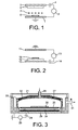
- FIG. 1 is a schematic view of an RF sputtering device according to the known art, for the growth of carbon nanotubes.
- the device comprises, in a deposition chamber, a first electrode 1 (cathode) acting as a sample holder and a second electrode 2 (anode) placed opposite.
- the electrode 2 supports, on its face facing the electrode 1, a graphite target 5.
- the electrode 1 supports, on its face facing the electrode 2, a sample 6 for receiving a deposit of nanotubes. Between the target 5 and the sample 6 is disposed near the sample, a filament 7 brought to temperature required to crack the graphite from the target.
- the present invention allows the growth of vertical carbon nanotubes on surfaces or devices using a solid carbon target, without the addition of hot filament.
- the subject of the invention is therefore a process for the growth of carbon nanotubes oriented on a sample using a target of carbon or a variety of carbon in a deposition chamber where a plasma is present, characterized in that the sample is disposed in contact of the target, so that the target has a free surface and the sample has a free surface, the plasma causing the growth of carbon nanotubes on the free surface of the sample.
- the plasma can be a hydrogen plasma. It may be a plasma of a gaseous mixture comprising hydrogen.
- the gaseous mixture may comprise at least one rare gas chosen, for example, from argon, krypton and xenon. It can include nitrogen or ammonia. It may include a carbonaceous gas such as CO or acetylene.
- the free surface offered by the sample supports, at least partially, a catalytic layer.
- the process can be carried out at a temperature above 300 ° C.
- the free surface of the target has a grid shape.
- the target may consist of a deposit made on the sample.
- the process according to the invention can be applied to the growth of carbon nanotubes on a substrate made of semiconductor material or glass. It can also be used to obtain the growth of carbon nanotubes oriented at the bottom of triode cavities of a field emission emitter plate, the carbon nanotubes then constituting electron emitting sources.
- FIG. 2 is a schematic view of a device for the growth of carbon nanotubes according to the invention.
- the device comprises, in a deposition chamber, a first electrode 11 (cathode) and a second electrode 12 (anode) placed vis-à-vis.
- the electrode 12 supports in stacking, on its face facing the electrode 11, a graphite target And a sample 16 for receiving a deposit of nanotubes.
- the target 15 has a free surface, that is to say not covered by the sample and the sample 16 provides a free surface for the growth of the nanotubes. In the enclosure reigns hydrogen plasma.
- Target 15 provides carbon input via plasma ion bombardment.
- the sample comprises, on its free surface, a catalytic deposit.
- a catalytic deposit Among the catalysts known to those skilled in the art, mention may be made of iron, cobalt, nickel, platinum and molybdenum.
- the growth of the nanotubes is then localized on the catalyst. Deposition is at a temperature typically greater than 300 ° C.
- the gas used to obtain the plasma may be pure hydrogen. It may also be a gaseous mixture comprising hydrogen and one or more rare gases chosen for example from argon, krypton and xenon. The mixture may also contain nitrogen or ammonia known to act at the carbon-crystal level. It may also contain a carbonaceous gas such as CO or acetylene.
- FIG. 3 is a cross-sectional diagram of a deposition chamber for carrying out the method according to the invention.
- This enclosure allows the realization of a secondary vacuum.
- a quartz bell 27 limits the reaction zone where the plasma is produced.
- This bell 27 allows the introduction of gas by a gas inlet 28.
- the bell rests on a sole 29 electrically isolated from the frame 21.
- a gas outlet 31 makes it possible to pump the inside of the frame 21.
- a first heating device 32 is disposed above the bell 27 and under a thermal reflector 33.
- a second heating device 34 placed in the lower position, heats the graphite target 25.
- the target 25 rests on the sole 29 and supports a sample 26 (or more samples). The target and the sample are therefore at the same electrical potential.
- FIG. 4 is a sectional view of a particular arrangement of a graphite target 45, in the form of a grid disposed on a sample 46.
- the sample 46 is, for example, a silicon wafer of 200 or 300 mm in diameter. This wafer includes active areas 47 to receive carbon nanotubes and separated by cutting paths 48 (typically 0.5 mm wide).
- the samples comprise a multilayer of materials deposited on a silicon substrate.
- a silicon substrate On the substrate, there is successively a titanium layer 60 nm thick, a TiN layer 65 nm thick and a nickel layer 3 nm thick.
- the sample is placed in the reaction chamber shown in FIG. 3. In this chamber, the sample is subjected to a temperature of 500 ° C, under a pressure of 150 mTorr (20 Pa) of hydrogen and for 20 minutes. A pure hydrogen plasma is then produced with a power of 300 W at a pressure of 150 mTorr (20 Pa). The deposition phase of the carbon nanotubes is carried out for 1 hour.
- FIG. 5 is a photograph, obtained by scanning electron microscopy, of the nanotubes obtained. These nanotubes are vertical. They have an average diameter of 36 nm and a height of 400 nm. The selectivity of the deposit is excellent. No parasitic carbon deposit is observed outside the catalyst grains.
- the samples comprise a multilayer of materials deposited on a silicon substrate. Triode structures are produced on this substrate in the following manner, with reference to FIG. 6.
- cavities are opened up to the layer 52 of TiN which plays the role of cathode conductor.
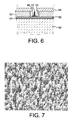
- FIG. 6 shows only one cavity 55.
- a nickel pellet 56 having a thickness of 3 nm is then localized by photolithography at the bottom of the cavity 55 and at its center.
- the sample is placed in the reaction chamber shown in FIG. 3.
- the sample is subjected to a temperature of 500 ° C. under a pressure of 150 mTorr (20 Pa) of pure hydrogen and for 20 minutes. minutes.
- a plasma containing 25% of argon and 75% of hydrogen is then produced with a power of 300 W.
- the deposition phase of the carbon nanotubes is carried out for 1 hour.
- a rod-shaped element 57 is thus formed, obtained by vertical growth of carbon nanotubes.
- the element 57 constitutes an electron-emitting source, the layers 51 and 52 acting as cathode conductors and the layer 54 acting as an extraction grid.
- argon with another gas known to promote spraying such as xenon or krypton for example.
- the samples comprise a multilayer of materials deposited on a borosilicate glass substrate.
- a borosilicate glass substrate On this substrate, there is successively a 200 nm thick layer of molybdenum, an amorphous silicon layer 1.4 ⁇ m thick, a TiN layer 65 nm thick and a 3 nm nickel layer. thick.
- the sample is placed in the reaction chamber shown in FIG. 3. In this chamber, the sample is subjected to a temperature of 500 ° C, under a pressure of 150 mTorr (20 Pa) of hydrogen and for 20 minutes. A pure hydrogen plasma is then produced at the same pressure with a power of 300 W for 10 minutes. Then, a plasma containing 95% hydrogen and 5% acetylene is produced for 15 minutes.
- FIG. 7 is a photograph, obtained by scanning electron microscopy, of the nanotubes obtained.
Landscapes
- Chemical & Material Sciences (AREA)
- Engineering & Computer Science (AREA)
- Materials Engineering (AREA)
- Organic Chemistry (AREA)
- Chemical Kinetics & Catalysis (AREA)
- Nanotechnology (AREA)
- Life Sciences & Earth Sciences (AREA)
- General Chemical & Material Sciences (AREA)
- Geochemistry & Mineralogy (AREA)
- Crystallography & Structural Chemistry (AREA)
- Metallurgy (AREA)
- Physics & Mathematics (AREA)
- Condensed Matter Physics & Semiconductors (AREA)
- General Physics & Mathematics (AREA)
- Composite Materials (AREA)
- Manufacturing & Machinery (AREA)
- Inorganic Chemistry (AREA)
- Mechanical Engineering (AREA)
- Carbon And Carbon Compounds (AREA)
- Cold Cathode And The Manufacture (AREA)
Applications Claiming Priority (1)
| Application Number | Priority Date | Filing Date | Title |
|---|---|---|---|
| FR0407529A FR2872826B1 (fr) | 2004-07-07 | 2004-07-07 | Croissance a basse temperature de nanotubes de carbone orientes |
Publications (3)
| Publication Number | Publication Date |
|---|---|
| EP1614765A2 true EP1614765A2 (de) | 2006-01-11 |
| EP1614765A3 EP1614765A3 (de) | 2006-05-03 |
| EP1614765B1 EP1614765B1 (de) | 2008-10-01 |
Family
ID=34947916
Family Applications (1)
| Application Number | Title | Priority Date | Filing Date |
|---|---|---|---|
| EP05106104A Expired - Lifetime EP1614765B1 (de) | 2004-07-07 | 2005-07-05 | Niedertemperaturwachstum orientierter Kohlenstoff-Nanoröhrchen |
Country Status (6)
| Country | Link |
|---|---|
| US (1) | US8034218B2 (de) |
| EP (1) | EP1614765B1 (de) |
| JP (1) | JP5014600B2 (de) |
| AT (1) | ATE409755T1 (de) |
| DE (1) | DE602005010003D1 (de) |
| FR (1) | FR2872826B1 (de) |
Families Citing this family (32)
| Publication number | Priority date | Publication date | Assignee | Title |
|---|---|---|---|---|
| FR2873852B1 (fr) * | 2004-07-28 | 2011-06-24 | Commissariat Energie Atomique | Structure de cathode a haute resolution |
| FR2897718B1 (fr) | 2006-02-22 | 2008-10-17 | Commissariat Energie Atomique | Structure de cathode a nanotubes pour ecran emissif |
| JP2007314391A (ja) * | 2006-05-29 | 2007-12-06 | Ulvac Japan Ltd | カーボンナノチューブ成長用基板及びその基板を用いたカーボンナノチューブの作製方法 |
| US9005755B2 (en) | 2007-01-03 | 2015-04-14 | Applied Nanostructured Solutions, Llc | CNS-infused carbon nanomaterials and process therefor |
| US8951631B2 (en) | 2007-01-03 | 2015-02-10 | Applied Nanostructured Solutions, Llc | CNT-infused metal fiber materials and process therefor |
| US8951632B2 (en) | 2007-01-03 | 2015-02-10 | Applied Nanostructured Solutions, Llc | CNT-infused carbon fiber materials and process therefor |
| US8158217B2 (en) | 2007-01-03 | 2012-04-17 | Applied Nanostructured Solutions, Llc | CNT-infused fiber and method therefor |
| US7847273B2 (en) * | 2007-03-30 | 2010-12-07 | Eloret Corporation | Carbon nanotube electron gun |
| JP5577356B2 (ja) | 2009-02-17 | 2014-08-20 | アプライド ナノストラクチャード ソリューションズ リミテッド ライアビリティー カンパニー | カーボン・ナノチューブを繊維上に含んで構成された複合材料 |
| CN102333906B (zh) | 2009-02-27 | 2015-03-11 | 应用纳米结构方案公司 | 使用气体预热法的低温cnt生长 |
| US20100227134A1 (en) | 2009-03-03 | 2010-09-09 | Lockheed Martin Corporation | Method for the prevention of nanoparticle agglomeration at high temperatures |
| US9111658B2 (en) | 2009-04-24 | 2015-08-18 | Applied Nanostructured Solutions, Llc | CNS-shielded wires |
| AU2010259173B2 (en) | 2009-04-24 | 2015-03-19 | Applied Nanostructured Solutions Llc | CNT-based signature control material |
| BRPI1014711A2 (pt) | 2009-04-27 | 2016-04-12 | Applied Nanostrctured Solutions Llc | aquecimento de resistência com base em cnt para descongelar estruturas de compósito |
| WO2011017200A1 (en) | 2009-08-03 | 2011-02-10 | Lockheed Martin Corporation | Incorporation of nanoparticles in composite fibers |
| EP2504164A4 (de) | 2009-11-23 | 2013-07-17 | Applied Nanostructured Sols | Keramikverbundmaterialien mit kohlenstoffnanoröhreninfundierten fasermaterialien sowie herstellungsverfahren dafür |
| CN102596715A (zh) | 2009-11-23 | 2012-07-18 | 应用纳米结构方案公司 | Cnt特制复合材料地面基结构 |
| KR20120104600A (ko) | 2009-12-14 | 2012-09-21 | 어플라이드 나노스트럭처드 솔루션스, 엘엘씨. | 탄소 나노튜브 주입된 섬유 물질을 포함하는 방염 복합재 물질 및 물품 |
| US9167736B2 (en) | 2010-01-15 | 2015-10-20 | Applied Nanostructured Solutions, Llc | CNT-infused fiber as a self shielding wire for enhanced power transmission line |
| AU2011256789A1 (en) | 2010-02-02 | 2012-07-12 | Applied Nanostructured Solutions, Llc | Fiber containing parallel-aligned carbon nanotubes |
| KR101818640B1 (ko) | 2010-03-02 | 2018-01-15 | 어플라이드 나노스트럭처드 솔루션스, 엘엘씨. | 카본 나노튜브 주입된 섬유를 포함하는 전기 장치 및 그의 제조 방법 |
| CA2790205A1 (en) | 2010-03-02 | 2011-09-09 | Applied Nanostructured Solutions, Llc | Spiral wound electrical devices containing carbon nanotube-infused electrode materials and methods and apparatuses for production thereof |
| US8780526B2 (en) | 2010-06-15 | 2014-07-15 | Applied Nanostructured Solutions, Llc | Electrical devices containing carbon nanotube-infused fibers and methods for production thereof |
| US9017854B2 (en) | 2010-08-30 | 2015-04-28 | Applied Nanostructured Solutions, Llc | Structural energy storage assemblies and methods for production thereof |
| BR112013005802A2 (pt) | 2010-09-14 | 2016-05-10 | Applied Nanostructured Sols | substratos de vidro com nanotubos de carbono crescidos sobre os mesmos e métodos para sua produção |
| AU2011305809A1 (en) | 2010-09-22 | 2013-02-28 | Applied Nanostructured Solutions, Llc | Carbon fiber substrates having carbon nanotubes grown thereon and processes for production thereof |
| EP2629595A2 (de) | 2010-09-23 | 2013-08-21 | Applied NanoStructured Solutions, LLC | CNT-infundierte Faser als selbstabschirmendes Kabel für eine Übertragungsleitung mit erhöhter Leistung |
| US9085464B2 (en) | 2012-03-07 | 2015-07-21 | Applied Nanostructured Solutions, Llc | Resistance measurement system and method of using the same |
| US10920085B2 (en) | 2016-01-20 | 2021-02-16 | Honda Motor Co., Ltd. | Alteration of carbon fiber surface properties via growing of carbon nanotubes |
| KR102652116B1 (ko) * | 2018-06-18 | 2024-03-29 | 어플라이드 머티어리얼스, 인코포레이티드 | 쌍을 이룬 동적 평행판 용량성 결합된 플라즈마들 |
| US10336618B1 (en) * | 2018-06-29 | 2019-07-02 | The Florida International University Board Of Trustees | Apparatus and method for synthesizing vertically aligned carbon nanotubes |
| US11476464B1 (en) | 2021-09-10 | 2022-10-18 | The Florida International University Board Of Trustees | Coated vertically aligned carbon nanotubes on nickel foam |
Family Cites Families (22)
| Publication number | Priority date | Publication date | Assignee | Title |
|---|---|---|---|---|
| US3708418A (en) * | 1970-03-05 | 1973-01-02 | Rca Corp | Apparatus for etching of thin layers of material by ion bombardment |
| AU664995B2 (en) * | 1991-04-19 | 1995-12-14 | Surface Solutions, Incorporated | Method and apparatus for linear magnetron sputtering |
| US5334199A (en) * | 1992-08-17 | 1994-08-02 | Inbae Yoon | Ligating instrument and methods of ligating tissue in endoscopic operative procedures |
| JP2526408B2 (ja) * | 1994-01-28 | 1996-08-21 | 工業技術院長 | カ―ボンナノチュ―ブの連続製造方法及び装置 |
| DE4405768A1 (de) * | 1994-02-23 | 1995-08-24 | Till Keesmann | Feldemissionskathodeneinrichtung und Verfahren zu ihrer Herstellung |
| JP3360415B2 (ja) * | 1994-05-24 | 2002-12-24 | 松下電工株式会社 | 回路パターン形成方法 |
| US5704943A (en) * | 1995-09-25 | 1998-01-06 | Yoon; Inbae | Ligating instrument with multiple loop ligature supply and methods therefor |
| JP3441923B2 (ja) * | 1997-06-18 | 2003-09-02 | キヤノン株式会社 | カーボンナノチューブの製法 |
| JP2001048512A (ja) * | 1999-08-04 | 2001-02-20 | Ulvac Japan Ltd | 垂直配向カーボンナノチューブの作製方法 |
| DE19946182C2 (de) * | 1999-09-21 | 2003-07-03 | Forschungsverbund Berlin Ev | Verfahren zur Herstellung von Kohlenstoff Nanoröhren |
| US6923946B2 (en) * | 1999-11-26 | 2005-08-02 | Ut-Battelle, Llc | Condensed phase conversion and growth of nanorods instead of from vapor |
| KR100480773B1 (ko) * | 2000-01-07 | 2005-04-06 | 삼성에스디아이 주식회사 | 카본 나노 튜브를 이용한 3극 전계방출소자의 제작방법 |
| EP1129990A1 (de) * | 2000-02-25 | 2001-09-05 | Lucent Technologies Inc. | Verfahren zum kontrolliertem Wachstum von Kohlenstoffnanoröhren |
| DE10103340A1 (de) * | 2001-01-25 | 2002-08-22 | Infineon Technologies Ag | Verfahren zum Wachsen von Kohlenstoff-Nanoröhren oberhalb einer elektrisch zu kontaktierenden Unterlage sowie Bauelement |
| US20020160111A1 (en) * | 2001-04-25 | 2002-10-31 | Yi Sun | Method for fabrication of field emission devices using carbon nanotube film as a cathode |
| JP2003137521A (ja) * | 2001-10-31 | 2003-05-14 | Ulvac Japan Ltd | 成膜方法 |
| SG106651A1 (en) * | 2001-11-27 | 2004-10-29 | Univ Nanyang | Field emission device and method of fabricating same |
| US7918867B2 (en) * | 2001-12-07 | 2011-04-05 | Abbott Laboratories | Suture trimmer |
| JP2003204966A (ja) * | 2002-01-16 | 2003-07-22 | Olympus Optical Co Ltd | 医療用結紮装置 |
| JP3621928B2 (ja) * | 2002-04-05 | 2005-02-23 | 浩史 滝川 | カーボンナノ微粒子の製造方法,カーボンナノ微粒子の製造装置 |
| AU2003264212A1 (en) * | 2002-09-17 | 2004-04-08 | Ht Innovative Technologies, Llc | Process of controllable synthesis of carbon films with composite structures |
| US7435251B2 (en) * | 2004-08-31 | 2008-10-14 | Green David T | System for securing a suture |
-
2004
- 2004-07-07 FR FR0407529A patent/FR2872826B1/fr not_active Expired - Fee Related
-
2005
- 2005-07-05 EP EP05106104A patent/EP1614765B1/de not_active Expired - Lifetime
- 2005-07-05 AT AT05106104T patent/ATE409755T1/de not_active IP Right Cessation
- 2005-07-05 DE DE602005010003T patent/DE602005010003D1/de not_active Expired - Lifetime
- 2005-07-06 JP JP2005198112A patent/JP5014600B2/ja not_active Expired - Fee Related
- 2005-07-06 US US11/174,537 patent/US8034218B2/en not_active Expired - Fee Related
Also Published As
| Publication number | Publication date |
|---|---|
| ATE409755T1 (de) | 2008-10-15 |
| EP1614765A3 (de) | 2006-05-03 |
| JP5014600B2 (ja) | 2012-08-29 |
| EP1614765B1 (de) | 2008-10-01 |
| US8034218B2 (en) | 2011-10-11 |
| FR2872826A1 (fr) | 2006-01-13 |
| JP2006052127A (ja) | 2006-02-23 |
| DE602005010003D1 (de) | 2008-11-13 |
| US20060177602A1 (en) | 2006-08-10 |
| FR2872826B1 (fr) | 2006-09-15 |
Similar Documents
| Publication | Publication Date | Title |
|---|---|---|
| EP1614765B1 (de) | Niedertemperaturwachstum orientierter Kohlenstoff-Nanoröhrchen | |
| EP2233435B1 (de) | Herstellungsverfahren von Graphen | |
| EP1341718B1 (de) | Verfahren und vorrichtung zum ecr plasma aufbringen von einwandigen kohlenstoffnanoröhren sowie erhaltene nanoröhren | |
| US20070103048A1 (en) | Method for fabricating carbon nanotube-based field emission device | |
| EP1451102A1 (de) | Verfahren zum katalytischen wachsenlassen von nanoröhrchen oder nanofasern mit einer diffusionsbarriere aus nisi-legierung | |
| EP1885909B1 (de) | Verfahren zur herstellung von nanostrukturen | |
| EP0005442B1 (de) | Verfahren und Vorrichtung zur Herstellung von Aluminiumnitrid, das für elektronische Anwendungen geeignet ist | |
| EP1365991B1 (de) | Verfahren zur bildung einer kohlenstoffnanoröhren enthaltenden beschichtung auf einem substrat | |
| Asano et al. | Field emission from ion‐milled diamond films on Si | |
| EP2856543B1 (de) | Verfahren zur herstellung einer elektrode, entsprechende elektrode und batterie mit derartiger elektrode | |
| FR2643192A1 (fr) | Procede de fabrication d'un dispositif semi-conducteur comprenant une electrode en metal refractaire sur un substrat semi-isolant | |
| JP2969503B2 (ja) | 炭素質ファイバーの作成方法 | |
| JPH0536847A (ja) | ダイヤモンド多層配線基板の製造方法 | |
| EP1323671A1 (de) | Verfahren zur Herstellung von mindestens eines Nanorohres zwischen zwei elektrisch leitenden Elementen sowie Vorrichtung zur Durchführung des Verfahrens | |
| KR20010039636A (ko) | 탄소나노튜브를 이용한 백색 광원 및 그 제조 방법 | |
| JP4907017B2 (ja) | カーボンナノチューブ膜体の製造方法 | |
| JP3372384B2 (ja) | プラズマcvd装置 | |
| FR2811686A1 (fr) | Procede de fabrication de couches de carbone aptes a emettre des electrons, par depot chimique en phase vapeur | |
| WO2005005685A2 (fr) | Croissance catalytique et directionnelle de nanotubes de carbone individuels, application a des sources froides d’electrons | |
| EP3818189A1 (de) | Verfahren und vorrichtung zur diamantsynthese durch cvd | |
| FR3018282A1 (fr) | Procede d'elaboration d'un film de graphene | |
| KR20220015411A (ko) | 개선된 반사 모드 다이노드 | |
| WO2021170739A1 (fr) | Procédé de réalisation d'une couche à base de nitrure d'aluminium (aln) sur une structure à base de silicium ou de matériaux iii-v | |
| Wisitsoraat et al. | Characterization of stackless vertically aligned carbon nanotube synthesized by thermal CVD with gravity effect and water-assisted etching | |
| FR2587732A1 (fr) | Reacteur de depot chimique en phase vapeur assiste par plasma |
Legal Events
| Date | Code | Title | Description |
|---|---|---|---|
| PUAI | Public reference made under article 153(3) epc to a published international application that has entered the european phase |
Free format text: ORIGINAL CODE: 0009012 |
|
| AK | Designated contracting states |
Kind code of ref document: A2 Designated state(s): AT BE BG CH CY CZ DE DK EE ES FI FR GB GR HU IE IS IT LI LT LU LV MC NL PL PT RO SE SI SK TR |
|
| AX | Request for extension of the european patent |
Extension state: AL BA HR MK YU |
|
| PUAL | Search report despatched |
Free format text: ORIGINAL CODE: 0009013 |
|
| AK | Designated contracting states |
Kind code of ref document: A3 Designated state(s): AT BE BG CH CY CZ DE DK EE ES FI FR GB GR HU IE IS IT LI LT LU LV MC NL PL PT RO SE SI SK TR |
|
| AX | Request for extension of the european patent |
Extension state: AL BA HR MK YU |
|
| RAP1 | Party data changed (applicant data changed or rights of an application transferred) |
Owner name: COMMISSARIAT A L'ENERGIE ATOMIQUE |
|
| 17P | Request for examination filed |
Effective date: 20061025 |
|
| AKX | Designation fees paid |
Designated state(s): AT BE BG CH CY CZ DE DK EE ES FI FR GB GR HU IE IS IT LI LT LU LV MC NL PL PT RO SE SI SK TR |
|
| GRAP | Despatch of communication of intention to grant a patent |
Free format text: ORIGINAL CODE: EPIDOSNIGR1 |
|
| GRAS | Grant fee paid |
Free format text: ORIGINAL CODE: EPIDOSNIGR3 |
|
| GRAA | (expected) grant |
Free format text: ORIGINAL CODE: 0009210 |
|
| AK | Designated contracting states |
Kind code of ref document: B1 Designated state(s): AT BE BG CH CY CZ DE DK EE ES FI FR GB GR HU IE IS IT LI LT LU LV MC NL PL PT RO SE SI SK TR |
|
| REG | Reference to a national code |
Ref country code: GB Ref legal event code: FG4D Free format text: NOT ENGLISH |
|
| REG | Reference to a national code |
Ref country code: CH Ref legal event code: EP |
|
| REG | Reference to a national code |
Ref country code: IE Ref legal event code: FG4D Free format text: LANGUAGE OF EP DOCUMENT: FRENCH |
|
| REF | Corresponds to: |
Ref document number: 602005010003 Country of ref document: DE Date of ref document: 20081113 Kind code of ref document: P |
|
| PG25 | Lapsed in a contracting state [announced via postgrant information from national office to epo] |
Ref country code: SI Free format text: LAPSE BECAUSE OF FAILURE TO SUBMIT A TRANSLATION OF THE DESCRIPTION OR TO PAY THE FEE WITHIN THE PRESCRIBED TIME-LIMIT Effective date: 20081001 |
|
| NLV1 | Nl: lapsed or annulled due to failure to fulfill the requirements of art. 29p and 29m of the patents act | ||
| REG | Reference to a national code |
Ref country code: IE Ref legal event code: FD4D |
|
| PG25 | Lapsed in a contracting state [announced via postgrant information from national office to epo] |
Ref country code: LT Free format text: LAPSE BECAUSE OF FAILURE TO SUBMIT A TRANSLATION OF THE DESCRIPTION OR TO PAY THE FEE WITHIN THE PRESCRIBED TIME-LIMIT Effective date: 20081001 Ref country code: AT Free format text: LAPSE BECAUSE OF FAILURE TO SUBMIT A TRANSLATION OF THE DESCRIPTION OR TO PAY THE FEE WITHIN THE PRESCRIBED TIME-LIMIT Effective date: 20081001 Ref country code: BG Free format text: LAPSE BECAUSE OF FAILURE TO SUBMIT A TRANSLATION OF THE DESCRIPTION OR TO PAY THE FEE WITHIN THE PRESCRIBED TIME-LIMIT Effective date: 20090101 Ref country code: ES Free format text: LAPSE BECAUSE OF FAILURE TO SUBMIT A TRANSLATION OF THE DESCRIPTION OR TO PAY THE FEE WITHIN THE PRESCRIBED TIME-LIMIT Effective date: 20090112 |
|
| PG25 | Lapsed in a contracting state [announced via postgrant information from national office to epo] |
Ref country code: NL Free format text: LAPSE BECAUSE OF FAILURE TO SUBMIT A TRANSLATION OF THE DESCRIPTION OR TO PAY THE FEE WITHIN THE PRESCRIBED TIME-LIMIT Effective date: 20081001 Ref country code: PT Free format text: LAPSE BECAUSE OF FAILURE TO SUBMIT A TRANSLATION OF THE DESCRIPTION OR TO PAY THE FEE WITHIN THE PRESCRIBED TIME-LIMIT Effective date: 20090302 Ref country code: FI Free format text: LAPSE BECAUSE OF FAILURE TO SUBMIT A TRANSLATION OF THE DESCRIPTION OR TO PAY THE FEE WITHIN THE PRESCRIBED TIME-LIMIT Effective date: 20081001 Ref country code: LV Free format text: LAPSE BECAUSE OF FAILURE TO SUBMIT A TRANSLATION OF THE DESCRIPTION OR TO PAY THE FEE WITHIN THE PRESCRIBED TIME-LIMIT Effective date: 20081001 Ref country code: PL Free format text: LAPSE BECAUSE OF FAILURE TO SUBMIT A TRANSLATION OF THE DESCRIPTION OR TO PAY THE FEE WITHIN THE PRESCRIBED TIME-LIMIT Effective date: 20081001 Ref country code: IS Free format text: LAPSE BECAUSE OF FAILURE TO SUBMIT A TRANSLATION OF THE DESCRIPTION OR TO PAY THE FEE WITHIN THE PRESCRIBED TIME-LIMIT Effective date: 20090201 |
|
| PG25 | Lapsed in a contracting state [announced via postgrant information from national office to epo] |
Ref country code: EE Free format text: LAPSE BECAUSE OF FAILURE TO SUBMIT A TRANSLATION OF THE DESCRIPTION OR TO PAY THE FEE WITHIN THE PRESCRIBED TIME-LIMIT Effective date: 20081001 Ref country code: IE Free format text: LAPSE BECAUSE OF FAILURE TO SUBMIT A TRANSLATION OF THE DESCRIPTION OR TO PAY THE FEE WITHIN THE PRESCRIBED TIME-LIMIT Effective date: 20081001 Ref country code: DK Free format text: LAPSE BECAUSE OF FAILURE TO SUBMIT A TRANSLATION OF THE DESCRIPTION OR TO PAY THE FEE WITHIN THE PRESCRIBED TIME-LIMIT Effective date: 20081001 Ref country code: RO Free format text: LAPSE BECAUSE OF FAILURE TO SUBMIT A TRANSLATION OF THE DESCRIPTION OR TO PAY THE FEE WITHIN THE PRESCRIBED TIME-LIMIT Effective date: 20081001 |
|
| PLBE | No opposition filed within time limit |
Free format text: ORIGINAL CODE: 0009261 |
|
| STAA | Information on the status of an ep patent application or granted ep patent |
Free format text: STATUS: NO OPPOSITION FILED WITHIN TIME LIMIT |
|
| PG25 | Lapsed in a contracting state [announced via postgrant information from national office to epo] |
Ref country code: SE Free format text: LAPSE BECAUSE OF FAILURE TO SUBMIT A TRANSLATION OF THE DESCRIPTION OR TO PAY THE FEE WITHIN THE PRESCRIBED TIME-LIMIT Effective date: 20090101 Ref country code: CZ Free format text: LAPSE BECAUSE OF FAILURE TO SUBMIT A TRANSLATION OF THE DESCRIPTION OR TO PAY THE FEE WITHIN THE PRESCRIBED TIME-LIMIT Effective date: 20081001 |
|
| 26N | No opposition filed |
Effective date: 20090702 |
|
| PG25 | Lapsed in a contracting state [announced via postgrant information from national office to epo] |
Ref country code: SK Free format text: LAPSE BECAUSE OF FAILURE TO SUBMIT A TRANSLATION OF THE DESCRIPTION OR TO PAY THE FEE WITHIN THE PRESCRIBED TIME-LIMIT Effective date: 20081001 |
|
| BERE | Be: lapsed |
Owner name: COMMISSARIAT A L'ENERGIE ATOMIQUE Effective date: 20090731 |
|
| PG25 | Lapsed in a contracting state [announced via postgrant information from national office to epo] |
Ref country code: MC Free format text: LAPSE BECAUSE OF NON-PAYMENT OF DUE FEES Effective date: 20090731 |
|
| REG | Reference to a national code |
Ref country code: CH Ref legal event code: PL |
|
| PG25 | Lapsed in a contracting state [announced via postgrant information from national office to epo] |
Ref country code: CH Free format text: LAPSE BECAUSE OF NON-PAYMENT OF DUE FEES Effective date: 20090731 Ref country code: LI Free format text: LAPSE BECAUSE OF NON-PAYMENT OF DUE FEES Effective date: 20090731 |
|
| PG25 | Lapsed in a contracting state [announced via postgrant information from national office to epo] |
Ref country code: BE Free format text: LAPSE BECAUSE OF NON-PAYMENT OF DUE FEES Effective date: 20090731 |
|
| PG25 | Lapsed in a contracting state [announced via postgrant information from national office to epo] |
Ref country code: GR Free format text: LAPSE BECAUSE OF FAILURE TO SUBMIT A TRANSLATION OF THE DESCRIPTION OR TO PAY THE FEE WITHIN THE PRESCRIBED TIME-LIMIT Effective date: 20090102 |
|
| PG25 | Lapsed in a contracting state [announced via postgrant information from national office to epo] |
Ref country code: LU Free format text: LAPSE BECAUSE OF NON-PAYMENT OF DUE FEES Effective date: 20090705 |
|
| PG25 | Lapsed in a contracting state [announced via postgrant information from national office to epo] |
Ref country code: HU Free format text: LAPSE BECAUSE OF FAILURE TO SUBMIT A TRANSLATION OF THE DESCRIPTION OR TO PAY THE FEE WITHIN THE PRESCRIBED TIME-LIMIT Effective date: 20090402 |
|
| PG25 | Lapsed in a contracting state [announced via postgrant information from national office to epo] |
Ref country code: TR Free format text: LAPSE BECAUSE OF FAILURE TO SUBMIT A TRANSLATION OF THE DESCRIPTION OR TO PAY THE FEE WITHIN THE PRESCRIBED TIME-LIMIT Effective date: 20081001 |
|
| PG25 | Lapsed in a contracting state [announced via postgrant information from national office to epo] |
Ref country code: CY Free format text: LAPSE BECAUSE OF FAILURE TO SUBMIT A TRANSLATION OF THE DESCRIPTION OR TO PAY THE FEE WITHIN THE PRESCRIBED TIME-LIMIT Effective date: 20081001 |
|
| PGFP | Annual fee paid to national office [announced via postgrant information from national office to epo] |
Ref country code: IT Payment date: 20130711 Year of fee payment: 9 |
|
| PG25 | Lapsed in a contracting state [announced via postgrant information from national office to epo] |
Ref country code: IT Free format text: LAPSE BECAUSE OF NON-PAYMENT OF DUE FEES Effective date: 20140705 |
|
| REG | Reference to a national code |
Ref country code: FR Ref legal event code: PLFP Year of fee payment: 12 |
|
| REG | Reference to a national code |
Ref country code: FR Ref legal event code: PLFP Year of fee payment: 13 |
|
| REG | Reference to a national code |
Ref country code: FR Ref legal event code: PLFP Year of fee payment: 14 |
|
| PGFP | Annual fee paid to national office [announced via postgrant information from national office to epo] |
Ref country code: FR Payment date: 20190731 Year of fee payment: 15 Ref country code: DE Payment date: 20190711 Year of fee payment: 15 |
|
| PGFP | Annual fee paid to national office [announced via postgrant information from national office to epo] |
Ref country code: GB Payment date: 20190719 Year of fee payment: 15 |
|
| REG | Reference to a national code |
Ref country code: DE Ref legal event code: R119 Ref document number: 602005010003 Country of ref document: DE |
|
| GBPC | Gb: european patent ceased through non-payment of renewal fee |
Effective date: 20200705 |
|
| PG25 | Lapsed in a contracting state [announced via postgrant information from national office to epo] |
Ref country code: FR Free format text: LAPSE BECAUSE OF NON-PAYMENT OF DUE FEES Effective date: 20200731 Ref country code: GB Free format text: LAPSE BECAUSE OF NON-PAYMENT OF DUE FEES Effective date: 20200705 |
|
| PG25 | Lapsed in a contracting state [announced via postgrant information from national office to epo] |
Ref country code: DE Free format text: LAPSE BECAUSE OF NON-PAYMENT OF DUE FEES Effective date: 20210202 |