EP1614957A2 - LED-Matrix hoher Dichte - Google Patents
LED-Matrix hoher Dichte Download PDFInfo
- Publication number
- EP1614957A2 EP1614957A2 EP05012851A EP05012851A EP1614957A2 EP 1614957 A2 EP1614957 A2 EP 1614957A2 EP 05012851 A EP05012851 A EP 05012851A EP 05012851 A EP05012851 A EP 05012851A EP 1614957 A2 EP1614957 A2 EP 1614957A2
- Authority
- EP
- European Patent Office
- Prior art keywords
- printed circuit
- circuit board
- leds
- led array
- apertures
- Prior art date
- Legal status (The legal status is an assumption and is not a legal conclusion. Google has not performed a legal analysis and makes no representation as to the accuracy of the status listed.)
- Granted
Links
Images
Classifications
-
- A—HUMAN NECESSITIES
- A01—AGRICULTURE; FORESTRY; ANIMAL HUSBANDRY; HUNTING; TRAPPING; FISHING
- A01G—HORTICULTURE; CULTIVATION OF VEGETABLES, FLOWERS, RICE, FRUIT, VINES, HOPS OR SEAWEED; FORESTRY; WATERING
- A01G13/00—Protection of plants
- A01G13/20—Protective coverings for plants
- A01G13/27—Protective coverings for plants protecting specific parts of plants, e.g. roots, trunks or fruits
-
- G—PHYSICS
- G02—OPTICS
- G02B—OPTICAL ELEMENTS, SYSTEMS OR APPARATUS
- G02B6/00—Light guides; Structural details of arrangements comprising light guides and other optical elements, e.g. couplings
- G02B6/24—Coupling light guides
- G02B6/42—Coupling light guides with opto-electronic elements
- G02B6/4201—Packages, e.g. shape, construction, internal or external details
- G02B6/4249—Packages, e.g. shape, construction, internal or external details comprising arrays of active devices and fibres
- G02B6/425—Optical features
-
- A—HUMAN NECESSITIES
- A01—AGRICULTURE; FORESTRY; ANIMAL HUSBANDRY; HUNTING; TRAPPING; FISHING
- A01G—HORTICULTURE; CULTIVATION OF VEGETABLES, FLOWERS, RICE, FRUIT, VINES, HOPS OR SEAWEED; FORESTRY; WATERING
- A01G13/00—Protection of plants
- A01G13/10—Devices for affording protection against animals, birds or other pests
-
- B—PERFORMING OPERATIONS; TRANSPORTING
- B65—CONVEYING; PACKING; STORING; HANDLING THIN OR FILAMENTARY MATERIAL
- B65D—CONTAINERS FOR STORAGE OR TRANSPORT OF ARTICLES OR MATERIALS, e.g. BAGS, BARRELS, BOTTLES, BOXES, CANS, CARTONS, CRATES, DRUMS, JARS, TANKS, HOPPERS, FORWARDING CONTAINERS; ACCESSORIES, CLOSURES, OR FITTINGS THEREFOR; PACKAGING ELEMENTS; PACKAGES
- B65D85/00—Containers, packaging elements or packages, specially adapted for particular articles or materials
- B65D85/30—Containers, packaging elements or packages, specially adapted for particular articles or materials for articles particularly sensitive to damage by shock or pressure
- B65D85/34—Containers, packaging elements or packages, specially adapted for particular articles or materials for articles particularly sensitive to damage by shock or pressure for fruit, e.g. apples, oranges or tomatoes
- B65D85/345—Containers, packaging elements or packages, specially adapted for particular articles or materials for articles particularly sensitive to damage by shock or pressure for fruit, e.g. apples, oranges or tomatoes having a meshed or apertured closure to allow contents to breathe
-
- B—PERFORMING OPERATIONS; TRANSPORTING
- B65—CONVEYING; PACKING; STORING; HANDLING THIN OR FILAMENTARY MATERIAL
- B65D—CONTAINERS FOR STORAGE OR TRANSPORT OF ARTICLES OR MATERIALS, e.g. BAGS, BARRELS, BOTTLES, BOXES, CANS, CARTONS, CRATES, DRUMS, JARS, TANKS, HOPPERS, FORWARDING CONTAINERS; ACCESSORIES, CLOSURES, OR FITTINGS THEREFOR; PACKAGING ELEMENTS; PACKAGES
- B65D85/00—Containers, packaging elements or packages, specially adapted for particular articles or materials
- B65D85/50—Containers, packaging elements or packages, specially adapted for particular articles or materials for living organisms, articles or materials sensitive to changes of environment or atmospheric conditions, e.g. land animals, birds, fish, water plants, non-aquatic plants, flower bulbs, cut flowers or foliage
- B65D85/52—Containers, packaging elements or packages, specially adapted for particular articles or materials for living organisms, articles or materials sensitive to changes of environment or atmospheric conditions, e.g. land animals, birds, fish, water plants, non-aquatic plants, flower bulbs, cut flowers or foliage for living plants; for growing bulbs
-
- F—MECHANICAL ENGINEERING; LIGHTING; HEATING; WEAPONS; BLASTING
- F21—LIGHTING
- F21K—NON-ELECTRIC LIGHT SOURCES USING LUMINESCENCE; LIGHT SOURCES USING ELECTROCHEMILUMINESCENCE; LIGHT SOURCES USING CHARGES OF COMBUSTIBLE MATERIAL; LIGHT SOURCES USING SEMICONDUCTOR DEVICES AS LIGHT-GENERATING ELEMENTS; LIGHT SOURCES NOT OTHERWISE PROVIDED FOR
- F21K9/00—Light sources using semiconductor devices as light-generating elements, e.g. using light-emitting diodes [LED] or lasers
-
- F—MECHANICAL ENGINEERING; LIGHTING; HEATING; WEAPONS; BLASTING
- F21—LIGHTING
- F21Y—INDEXING SCHEME ASSOCIATED WITH SUBCLASSES F21K, F21L, F21S and F21V, RELATING TO THE FORM OR THE KIND OF THE LIGHT SOURCES OR OF THE COLOUR OF THE LIGHT EMITTED
- F21Y2105/00—Planar light sources
- F21Y2105/10—Planar light sources comprising a two-dimensional [2D] array of point-like light-generating elements
-
- F—MECHANICAL ENGINEERING; LIGHTING; HEATING; WEAPONS; BLASTING
- F21—LIGHTING
- F21Y—INDEXING SCHEME ASSOCIATED WITH SUBCLASSES F21K, F21L, F21S and F21V, RELATING TO THE FORM OR THE KIND OF THE LIGHT SOURCES OR OF THE COLOUR OF THE LIGHT EMITTED
- F21Y2107/00—Light sources with three-dimensionally disposed light-generating elements
- F21Y2107/60—Light sources with three-dimensionally disposed light-generating elements on stacked substrates
-
- F—MECHANICAL ENGINEERING; LIGHTING; HEATING; WEAPONS; BLASTING
- F21—LIGHTING
- F21Y—INDEXING SCHEME ASSOCIATED WITH SUBCLASSES F21K, F21L, F21S and F21V, RELATING TO THE FORM OR THE KIND OF THE LIGHT SOURCES OR OF THE COLOUR OF THE LIGHT EMITTED
- F21Y2115/00—Light-generating elements of semiconductor light sources
- F21Y2115/10—Light-emitting diodes [LED]
-
- H—ELECTRICITY
- H05—ELECTRIC TECHNIQUES NOT OTHERWISE PROVIDED FOR
- H05K—PRINTED CIRCUITS; CASINGS OR CONSTRUCTIONAL DETAILS OF ELECTRIC APPARATUS; MANUFACTURE OF ASSEMBLAGES OF ELECTRICAL COMPONENTS
- H05K1/00—Printed circuits
- H05K1/02—Details
- H05K1/14—Structural association of two or more printed circuits
- H05K1/144—Stacked arrangements of planar printed circuit boards
-
- H—ELECTRICITY
- H05—ELECTRIC TECHNIQUES NOT OTHERWISE PROVIDED FOR
- H05K—PRINTED CIRCUITS; CASINGS OR CONSTRUCTIONAL DETAILS OF ELECTRIC APPARATUS; MANUFACTURE OF ASSEMBLAGES OF ELECTRICAL COMPONENTS
- H05K1/00—Printed circuits
- H05K1/18—Printed circuits structurally associated with non-printed electric components
- H05K1/182—Printed circuits structurally associated with non-printed electric components associated with components mounted in printed circuit boards [PCB], e.g. insert-mounted components [IMC]
Definitions
- This invention relates to light sources and more particularly to light sources employing light emitting diodes (LED or LEDs). Still more particularly it relates to a lamp having a high density LED array.
- LED light emitting diodes
- LED lamps have been achieving acceptance as replacements for the more common incandescent types of lamps because of their long life and reasonable power requirements. These uses are particlulary present in the automotive industry where lamps employing LEDs have been used as taillights and as stoplights, such as the required center high mount stoplight (CHMSL).
- CHMSL center high mount stoplight
- the LEDs are solid state devices whose light output has increased over time, when driven at the power requirements necessary for some application, such as the aforementioned auto uses, the heat generated by the lamps becomes a problem requiring heat shields or heat dissipating additions, which increase the cost of the lamps.
- the density of the LED sources increases as a function of increasing the light output of a lamp, for example, to use LEDs in headlight applications, the heat generated becomes a significant problem. Also, stacking density of the LEDs becomes a physical problem in and of itself.
- a high-density LED array capable of presenting a density of X LEDs/unit area that comprises a first printed circuit board having X/2 LEDs/unit area and X/2/unit area apertures arrayed therewith; and a second printed circuit board spaced from said first printed circuit board and having X/2 LEDs/unit area, said LEDs on said second printed circuit board being aligned with said apertures in said first printed circuit board.
- both sets of LEDs can be associated with light guides, which can be directed to a remote location to provide special effects.
- the light guides can be plastic or glass or they can comprise optical fibers.
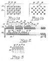
- Fig. 1a is a diagrammatic plan view of a first printed circuit board for use with the invention
- Fig. 1b is a similar view of a second printed circuit board
- Fig. 2 is a diagrammatic sectional elevational view of an LED lamp in accordance with an aspect of the invention.
- Fig 3 is a perspective view of one version of an optical fiber bundle.
- a high-density LED array 10 capable of presenting a density of X LEDs/unit area comprising a first printed circuit board 12 having a first surface 14 with X/2 LEDs 18/unit area and X/2 apertures 20 arrayed therewith.
- the printed circuit board 12 can be formed of two layers (see Fig. 2), a first layer 12a comprising a thermally conductive, electrically insulating material having conductive traces 12b thereon, bonded to a metal plate 12c, which functions as a heatsink.
- the metal plate 12c can have a depending leg 12d to further draw heat away from the operating LEDs.
- a second printed circuit board 22 has a surface 23 and can also be formed in two layers, a first layer 22a comprising a thermally conductive, electrically insulating material having conductive traces 22b thereon, bonded to a metal plate 22c which functions as a heatsink, and can further be provided with a depending leg 22d.
- the second PCB 22 is spaced from the the first PCB 12 and has X/2 LEDs 28/unit area. The LEDs 28 on the second printed circuit board are aligned with the apertures 20 in the first printed circuit board 14.
- the PCBs 12 and 22 are provided with a pattern of LEDs and apertures (PCB 12)or just LEDs (PCB 22). As shown the pattern is grid-like, comparable to a checkerboard pattern, and PCB 12 has alternate LEDs and apertures, while PCB 22 has only LEDs. Other patterns are of course possible, depending on the end use of the lamp with which the LED array will be used.
- Each of the LEDs 28 on the second printed circuit board 22 has a light guide 30 associated therewith and each of the light guides 30 extends through one of the apertures 20. Thus, all of the illumination from the LEDs 18 and the LEDs 28 appears to be in the same plane.
- the LEDs 18 can be provided with light guides 32 and all of the guides 30 and 32 can be bundled and directed to a remote location, in a group as shown diagrammatically in Fig. 3, or in any other desired configuration.
Landscapes
- Engineering & Computer Science (AREA)
- Physics & Mathematics (AREA)
- Life Sciences & Earth Sciences (AREA)
- Optics & Photonics (AREA)
- General Health & Medical Sciences (AREA)
- Toxicology (AREA)
- Health & Medical Sciences (AREA)
- Microelectronics & Electronic Packaging (AREA)
- Mechanical Engineering (AREA)
- Zoology (AREA)
- General Physics & Mathematics (AREA)
- Environmental Sciences (AREA)
- General Engineering & Computer Science (AREA)
- Botany (AREA)
- Evolutionary Biology (AREA)
- Marine Sciences & Fisheries (AREA)
- Birds (AREA)
- Fastening Of Light Sources Or Lamp Holders (AREA)
- Arrangement Of Elements, Cooling, Sealing, Or The Like Of Lighting Devices (AREA)
- Optical Couplings Of Light Guides (AREA)
- Non-Portable Lighting Devices Or Systems Thereof (AREA)
- Devices For Indicating Variable Information By Combining Individual Elements (AREA)
- Luminescent Compositions (AREA)
- Led Device Packages (AREA)
Applications Claiming Priority (2)
| Application Number | Priority Date | Filing Date | Title |
|---|---|---|---|
| US58052604P | 2004-06-17 | 2004-06-17 | |
| US10/984,457 US7090386B2 (en) | 2004-06-17 | 2004-11-09 | High density LED array |
Publications (3)
| Publication Number | Publication Date |
|---|---|
| EP1614957A2 true EP1614957A2 (de) | 2006-01-11 |
| EP1614957A3 EP1614957A3 (de) | 2007-09-12 |
| EP1614957B1 EP1614957B1 (de) | 2010-06-09 |
Family
ID=35311826
Family Applications (1)
| Application Number | Title | Priority Date | Filing Date |
|---|---|---|---|
| EP05012851A Ceased EP1614957B1 (de) | 2004-06-17 | 2005-06-15 | LED-Matrix hoher Dichte |
Country Status (7)
| Country | Link |
|---|---|
| US (1) | US7090386B2 (de) |
| EP (1) | EP1614957B1 (de) |
| JP (1) | JP4515967B2 (de) |
| KR (1) | KR20060045630A (de) |
| AT (1) | ATE470820T1 (de) |
| CA (1) | CA2498126C (de) |
| DE (1) | DE602005021725D1 (de) |
Cited By (1)
| Publication number | Priority date | Publication date | Assignee | Title |
|---|---|---|---|---|
| US10379277B2 (en) | 2006-09-13 | 2019-08-13 | Ideal Industries Lighting Llc | Lighting device |
Families Citing this family (12)
| Publication number | Priority date | Publication date | Assignee | Title |
|---|---|---|---|---|
| KR100644632B1 (ko) * | 2004-10-01 | 2006-11-10 | 삼성전자주식회사 | Led를 채용한 조명유닛 및 이를 채용한 화상투사장치 |
| US20070121333A1 (en) * | 2005-11-30 | 2007-05-31 | Ronald Woodward | Semiconductor light engine for automotive lighting |
| DE102006001490A1 (de) * | 2006-01-11 | 2007-07-12 | Patent-Treuhand-Gesellschaft für elektrische Glühlampen mbH | Beleuchtungseinrichtung |
| US20080025040A1 (en) * | 2006-07-25 | 2008-01-31 | Swantner Michael J | LED light engine |
| JP4544316B2 (ja) * | 2008-03-10 | 2010-09-15 | セイコーエプソン株式会社 | 光源及び光源実装方法 |
| JP5548213B2 (ja) * | 2008-12-09 | 2014-07-16 | コーニンクレッカ フィリップス エヌ ヴェ | ファイバ拡散要素を備えている照明システム |
| KR101198849B1 (ko) * | 2010-06-30 | 2012-11-07 | (주)포인트엔지니어링 | 광소자 디바이스 |
| US10088122B1 (en) * | 2017-08-04 | 2018-10-02 | Jute Industrial Co., Ltd. | Integrated lamp |
| JP7270342B2 (ja) * | 2018-06-12 | 2023-05-10 | 三菱電機株式会社 | 光源ユニットおよび照明装置 |
| KR102045676B1 (ko) * | 2018-06-21 | 2019-11-15 | 케이알에코스타 주식회사 | 향상된 해상도를 갖는 투명 디스플레이 |
| DE102019204523B4 (de) * | 2019-03-29 | 2023-08-03 | Edag Engineering Gmbh | Pixellichtmodul für eine Rückleuchte eines Fahrzeugs |
| US12331897B2 (en) * | 2023-11-17 | 2025-06-17 | Jute Industrial Co., Ltd. | Vehicle light |
Family Cites Families (17)
| Publication number | Priority date | Publication date | Assignee | Title |
|---|---|---|---|---|
| US3744048A (en) * | 1971-09-01 | 1973-07-03 | Ultronic Systems Corp | Display apparatus employing fiber optics |
| US4280122A (en) * | 1980-06-30 | 1981-07-21 | Dolan-Jenner Industries, Inc. | Optical fibers |
| US4525711A (en) * | 1982-09-03 | 1985-06-25 | Gery Alan R | Three-dimensional fiber optic display |
| US5293437A (en) * | 1992-06-03 | 1994-03-08 | Visual Optics, Inc. | Fiber optic display with direct driven optical fibers |
| JP3517472B2 (ja) * | 1995-03-02 | 2004-04-12 | 富士写真フイルム株式会社 | プリント用ヘッド装置 |
| US5911024A (en) * | 1997-04-07 | 1999-06-08 | Wallace; Troy B. | Fiber optic display screen assembly and method for making a fiber optic screen |
| JP2000021206A (ja) * | 1998-07-02 | 2000-01-21 | Ccs Kk | 照明装置 |
| JP2001118411A (ja) * | 1999-10-20 | 2001-04-27 | Ichikoh Ind Ltd | 車両用灯具 |
| US6527411B1 (en) * | 2000-08-01 | 2003-03-04 | Visteon Corporation | Collimating lamp |
| US20040146256A1 (en) * | 2000-09-19 | 2004-07-29 | Alexander Solntsev | Fiber optic real time display system |
| US6628867B1 (en) * | 2000-09-19 | 2003-09-30 | Alexander Solntsev | Fiber optic real time display system |
| DE20111814U1 (de) * | 2001-07-17 | 2001-11-15 | Müller, Walter, Dr., 07745 Jena | Lichthärtgerät zur Aushärtung von Zahnfüllmaterialien |
| US6921920B2 (en) * | 2001-08-31 | 2005-07-26 | Smith & Nephew, Inc. | Solid-state light source |
| DE10149837A1 (de) * | 2001-10-10 | 2003-05-08 | Siemens Ag | Anzeigevorrichtung |
| US6826336B2 (en) * | 2002-05-22 | 2004-11-30 | The Boeing Company | Fiber optic LED illuminator |
| CA2511761A1 (en) * | 2002-11-19 | 2004-06-03 | Den-Mat Corporation | Dental light guide |
| US6880276B2 (en) * | 2003-06-16 | 2005-04-19 | Walter Strein | Transparent electronic illuminated display |
-
2004
- 2004-11-09 US US10/984,457 patent/US7090386B2/en not_active Expired - Lifetime
-
2005
- 2005-02-23 CA CA2498126A patent/CA2498126C/en not_active Expired - Fee Related
- 2005-04-12 KR KR1020050030408A patent/KR20060045630A/ko not_active Withdrawn
- 2005-06-15 AT AT05012851T patent/ATE470820T1/de not_active IP Right Cessation
- 2005-06-15 EP EP05012851A patent/EP1614957B1/de not_active Ceased
- 2005-06-15 DE DE602005021725T patent/DE602005021725D1/de not_active Expired - Lifetime
- 2005-06-15 JP JP2005175091A patent/JP4515967B2/ja not_active Expired - Fee Related
Non-Patent Citations (1)
| Title |
|---|
| None |
Cited By (1)
| Publication number | Priority date | Publication date | Assignee | Title |
|---|---|---|---|---|
| US10379277B2 (en) | 2006-09-13 | 2019-08-13 | Ideal Industries Lighting Llc | Lighting device |
Also Published As
| Publication number | Publication date |
|---|---|
| DE602005021725D1 (de) | 2010-07-22 |
| CA2498126C (en) | 2012-07-31 |
| JP2006004936A (ja) | 2006-01-05 |
| EP1614957A3 (de) | 2007-09-12 |
| ATE470820T1 (de) | 2010-06-15 |
| EP1614957B1 (de) | 2010-06-09 |
| JP4515967B2 (ja) | 2010-08-04 |
| CA2498126A1 (en) | 2005-12-17 |
| US7090386B2 (en) | 2006-08-15 |
| US20050281025A1 (en) | 2005-12-22 |
| KR20060045630A (ko) | 2006-05-17 |
Similar Documents
| Publication | Publication Date | Title |
|---|---|---|
| JP5851017B2 (ja) | 複数の発光素子を実装するための基板 | |
| JP5081307B2 (ja) | 光学部位置決め装置 | |
| EP1710487B1 (de) | Dreifarbige LED-Lampenbirne | |
| CA2498126C (en) | High density led array | |
| CN105987337B (zh) | 用于机动车辆的包括两个光导和具有两个安装表面的散热器的光模块 | |
| KR100875961B1 (ko) | 발광 다이오드를 이용한 어레이 광원 및 이를 포함하는백라이트 유닛 | |
| US20050281033A1 (en) | LED automotive headlamp | |
| US20100053956A1 (en) | Light emitting module | |
| JP2007513378A (ja) | 固体光デバイス | |
| US20070291503A1 (en) | Light-Emitting Diode Arrangement for a High-Power Ligth-Emitting Diode and Method for Producing a Light-Emitting Diode Arrangement | |
| JP5391451B2 (ja) | 発光モジュール | |
| EP3242074B1 (de) | Lampeneinheit und fahrzeuglampenvorrichtung damit | |
| CN1914455B (zh) | 可变形的照明模块 | |
| CN1847721A (zh) | 虚点光源 | |
| US20090218586A1 (en) | Led lamp | |
| JP2007280739A (ja) | 照明用ledラインランプ | |
| JP7297431B2 (ja) | 回路基板及び車両用灯具 | |
| EP1760391A2 (de) | Lampe mit Licht emittierenden Dioden | |
| US20110019415A1 (en) | Heat dissipating module of light emitting diode | |
| KR20220032083A (ko) | 발광 엘리먼트들을 위한 지지체 및 라이팅 디바이스 | |
| JP6130412B2 (ja) | 発光構造体 | |
| JP7489997B2 (ja) | 自動車両の照明装置 | |
| KR102263966B1 (ko) | Led 패키지용 기판 장치 | |
| KR200396953Y1 (ko) | 발광 다이오드 모듈 | |
| JP2020035594A (ja) | 光源基板及び照明装置 |
Legal Events
| Date | Code | Title | Description |
|---|---|---|---|
| PUAI | Public reference made under article 153(3) epc to a published international application that has entered the european phase |
Free format text: ORIGINAL CODE: 0009012 |
|
| AK | Designated contracting states |
Kind code of ref document: A2 Designated state(s): AT BE BG CH CY CZ DE DK EE ES FI FR GB GR HU IE IS IT LI LT LU MC NL PL PT RO SE SI SK TR |
|
| AX | Request for extension of the european patent |
Extension state: AL BA HR LV MK YU |
|
| PUAL | Search report despatched |
Free format text: ORIGINAL CODE: 0009013 |
|
| AK | Designated contracting states |
Kind code of ref document: A3 Designated state(s): AT BE BG CH CY CZ DE DK EE ES FI FR GB GR HU IE IS IT LI LT LU MC NL PL PT RO SE SI SK TR |
|
| AX | Request for extension of the european patent |
Extension state: AL BA HR LV MK YU |
|
| 17P | Request for examination filed |
Effective date: 20080306 |
|
| AKX | Designation fees paid |
Designated state(s): AT BE BG CH CY CZ DE DK EE ES FI FR GB GR HU IE IS IT LI LT LU MC NL PL PT RO SE SI SK TR |
|
| 17Q | First examination report despatched |
Effective date: 20080507 |
|
| GRAP | Despatch of communication of intention to grant a patent |
Free format text: ORIGINAL CODE: EPIDOSNIGR1 |
|
| GRAS | Grant fee paid |
Free format text: ORIGINAL CODE: EPIDOSNIGR3 |
|
| GRAA | (expected) grant |
Free format text: ORIGINAL CODE: 0009210 |
|
| AK | Designated contracting states |
Kind code of ref document: B1 Designated state(s): AT BE BG CH CY CZ DE DK EE ES FI FR GB GR HU IE IS IT LI LT LU MC NL PL PT RO SE SI SK TR |
|
| REG | Reference to a national code |
Ref country code: CH Ref legal event code: EP |
|
| REG | Reference to a national code |
Ref country code: IE Ref legal event code: FG4D |
|
| REF | Corresponds to: |
Ref document number: 602005021725 Country of ref document: DE Date of ref document: 20100722 Kind code of ref document: P |
|
| REG | Reference to a national code |
Ref country code: NL Ref legal event code: VDEP Effective date: 20100609 |
|
| PG25 | Lapsed in a contracting state [announced via postgrant information from national office to epo] |
Ref country code: SE Free format text: LAPSE BECAUSE OF FAILURE TO SUBMIT A TRANSLATION OF THE DESCRIPTION OR TO PAY THE FEE WITHIN THE PRESCRIBED TIME-LIMIT Effective date: 20100609 Ref country code: LT Free format text: LAPSE BECAUSE OF FAILURE TO SUBMIT A TRANSLATION OF THE DESCRIPTION OR TO PAY THE FEE WITHIN THE PRESCRIBED TIME-LIMIT Effective date: 20100609 |
|
| LTIE | Lt: invalidation of european patent or patent extension |
Effective date: 20100609 |
|
| PG25 | Lapsed in a contracting state [announced via postgrant information from national office to epo] |
Ref country code: FI Free format text: LAPSE BECAUSE OF FAILURE TO SUBMIT A TRANSLATION OF THE DESCRIPTION OR TO PAY THE FEE WITHIN THE PRESCRIBED TIME-LIMIT Effective date: 20100609 Ref country code: AT Free format text: LAPSE BECAUSE OF FAILURE TO SUBMIT A TRANSLATION OF THE DESCRIPTION OR TO PAY THE FEE WITHIN THE PRESCRIBED TIME-LIMIT Effective date: 20100609 Ref country code: SI Free format text: LAPSE BECAUSE OF FAILURE TO SUBMIT A TRANSLATION OF THE DESCRIPTION OR TO PAY THE FEE WITHIN THE PRESCRIBED TIME-LIMIT Effective date: 20100609 |
|
| PG25 | Lapsed in a contracting state [announced via postgrant information from national office to epo] |
Ref country code: PL Free format text: LAPSE BECAUSE OF FAILURE TO SUBMIT A TRANSLATION OF THE DESCRIPTION OR TO PAY THE FEE WITHIN THE PRESCRIBED TIME-LIMIT Effective date: 20100609 Ref country code: GR Free format text: LAPSE BECAUSE OF FAILURE TO SUBMIT A TRANSLATION OF THE DESCRIPTION OR TO PAY THE FEE WITHIN THE PRESCRIBED TIME-LIMIT Effective date: 20100910 Ref country code: CY Free format text: LAPSE BECAUSE OF FAILURE TO SUBMIT A TRANSLATION OF THE DESCRIPTION OR TO PAY THE FEE WITHIN THE PRESCRIBED TIME-LIMIT Effective date: 20100609 |
|
| PG25 | Lapsed in a contracting state [announced via postgrant information from national office to epo] |
Ref country code: NL Free format text: LAPSE BECAUSE OF FAILURE TO SUBMIT A TRANSLATION OF THE DESCRIPTION OR TO PAY THE FEE WITHIN THE PRESCRIBED TIME-LIMIT Effective date: 20100609 Ref country code: MC Free format text: LAPSE BECAUSE OF NON-PAYMENT OF DUE FEES Effective date: 20100630 Ref country code: EE Free format text: LAPSE BECAUSE OF FAILURE TO SUBMIT A TRANSLATION OF THE DESCRIPTION OR TO PAY THE FEE WITHIN THE PRESCRIBED TIME-LIMIT Effective date: 20100609 |
|
| REG | Reference to a national code |
Ref country code: CH Ref legal event code: PL |
|
| PG25 | Lapsed in a contracting state [announced via postgrant information from national office to epo] |
Ref country code: SK Free format text: LAPSE BECAUSE OF FAILURE TO SUBMIT A TRANSLATION OF THE DESCRIPTION OR TO PAY THE FEE WITHIN THE PRESCRIBED TIME-LIMIT Effective date: 20100609 Ref country code: BE Free format text: LAPSE BECAUSE OF FAILURE TO SUBMIT A TRANSLATION OF THE DESCRIPTION OR TO PAY THE FEE WITHIN THE PRESCRIBED TIME-LIMIT Effective date: 20100609 Ref country code: CZ Free format text: LAPSE BECAUSE OF FAILURE TO SUBMIT A TRANSLATION OF THE DESCRIPTION OR TO PAY THE FEE WITHIN THE PRESCRIBED TIME-LIMIT Effective date: 20100609 Ref country code: IS Free format text: LAPSE BECAUSE OF FAILURE TO SUBMIT A TRANSLATION OF THE DESCRIPTION OR TO PAY THE FEE WITHIN THE PRESCRIBED TIME-LIMIT Effective date: 20101009 Ref country code: PT Free format text: LAPSE BECAUSE OF FAILURE TO SUBMIT A TRANSLATION OF THE DESCRIPTION OR TO PAY THE FEE WITHIN THE PRESCRIBED TIME-LIMIT Effective date: 20101011 Ref country code: RO Free format text: LAPSE BECAUSE OF FAILURE TO SUBMIT A TRANSLATION OF THE DESCRIPTION OR TO PAY THE FEE WITHIN THE PRESCRIBED TIME-LIMIT Effective date: 20100609 |
|
| PG25 | Lapsed in a contracting state [announced via postgrant information from national office to epo] |
Ref country code: IT Free format text: LAPSE BECAUSE OF FAILURE TO SUBMIT A TRANSLATION OF THE DESCRIPTION OR TO PAY THE FEE WITHIN THE PRESCRIBED TIME-LIMIT Effective date: 20100609 |
|
| PLBE | No opposition filed within time limit |
Free format text: ORIGINAL CODE: 0009261 |
|
| STAA | Information on the status of an ep patent application or granted ep patent |
Free format text: STATUS: NO OPPOSITION FILED WITHIN TIME LIMIT |
|
| PG25 | Lapsed in a contracting state [announced via postgrant information from national office to epo] |
Ref country code: LI Free format text: LAPSE BECAUSE OF NON-PAYMENT OF DUE FEES Effective date: 20100630 Ref country code: CH Free format text: LAPSE BECAUSE OF NON-PAYMENT OF DUE FEES Effective date: 20100630 Ref country code: IE Free format text: LAPSE BECAUSE OF NON-PAYMENT OF DUE FEES Effective date: 20100615 Ref country code: DK Free format text: LAPSE BECAUSE OF FAILURE TO SUBMIT A TRANSLATION OF THE DESCRIPTION OR TO PAY THE FEE WITHIN THE PRESCRIBED TIME-LIMIT Effective date: 20100609 |
|
| 26N | No opposition filed |
Effective date: 20110310 |
|
| REG | Reference to a national code |
Ref country code: DE Ref legal event code: R097 Ref document number: 602005021725 Country of ref document: DE Effective date: 20110309 |
|
| REG | Reference to a national code |
Ref country code: DE Ref legal event code: R082 Ref document number: 602005021725 Country of ref document: DE Representative=s name: PETER ZEDLITZ, DE Ref country code: DE Ref legal event code: R082 Ref document number: 602005021725 Country of ref document: DE Representative=s name: ZEDLITZ, PETER, DIPL.-INF. UNIV., DE |
|
| PG25 | Lapsed in a contracting state [announced via postgrant information from national office to epo] |
Ref country code: LU Free format text: LAPSE BECAUSE OF NON-PAYMENT OF DUE FEES Effective date: 20100615 Ref country code: HU Free format text: LAPSE BECAUSE OF FAILURE TO SUBMIT A TRANSLATION OF THE DESCRIPTION OR TO PAY THE FEE WITHIN THE PRESCRIBED TIME-LIMIT Effective date: 20101210 Ref country code: BG Free format text: LAPSE BECAUSE OF FAILURE TO SUBMIT A TRANSLATION OF THE DESCRIPTION OR TO PAY THE FEE WITHIN THE PRESCRIBED TIME-LIMIT Effective date: 20100609 |
|
| PG25 | Lapsed in a contracting state [announced via postgrant information from national office to epo] |
Ref country code: TR Free format text: LAPSE BECAUSE OF FAILURE TO SUBMIT A TRANSLATION OF THE DESCRIPTION OR TO PAY THE FEE WITHIN THE PRESCRIBED TIME-LIMIT Effective date: 20100609 |
|
| PG25 | Lapsed in a contracting state [announced via postgrant information from national office to epo] |
Ref country code: BG Free format text: LAPSE BECAUSE OF FAILURE TO SUBMIT A TRANSLATION OF THE DESCRIPTION OR TO PAY THE FEE WITHIN THE PRESCRIBED TIME-LIMIT Effective date: 20100909 |
|
| PG25 | Lapsed in a contracting state [announced via postgrant information from national office to epo] |
Ref country code: ES Free format text: LAPSE BECAUSE OF FAILURE TO SUBMIT A TRANSLATION OF THE DESCRIPTION OR TO PAY THE FEE WITHIN THE PRESCRIBED TIME-LIMIT Effective date: 20100920 |
|
| REG | Reference to a national code |
Ref country code: FR Ref legal event code: PLFP Year of fee payment: 12 |
|
| REG | Reference to a national code |
Ref country code: FR Ref legal event code: PLFP Year of fee payment: 13 |
|
| REG | Reference to a national code |
Ref country code: FR Ref legal event code: PLFP Year of fee payment: 14 |
|
| PGFP | Annual fee paid to national office [announced via postgrant information from national office to epo] |
Ref country code: DE Payment date: 20180625 Year of fee payment: 14 |
|
| PGFP | Annual fee paid to national office [announced via postgrant information from national office to epo] |
Ref country code: FR Payment date: 20180626 Year of fee payment: 14 |
|
| PGFP | Annual fee paid to national office [announced via postgrant information from national office to epo] |
Ref country code: GB Payment date: 20180620 Year of fee payment: 14 |
|
| REG | Reference to a national code |
Ref country code: DE Ref legal event code: R119 Ref document number: 602005021725 Country of ref document: DE |
|
| GBPC | Gb: european patent ceased through non-payment of renewal fee |
Effective date: 20190615 |
|
| PG25 | Lapsed in a contracting state [announced via postgrant information from national office to epo] |
Ref country code: DE Free format text: LAPSE BECAUSE OF NON-PAYMENT OF DUE FEES Effective date: 20200101 Ref country code: GB Free format text: LAPSE BECAUSE OF NON-PAYMENT OF DUE FEES Effective date: 20190615 |
|
| PG25 | Lapsed in a contracting state [announced via postgrant information from national office to epo] |
Ref country code: FR Free format text: LAPSE BECAUSE OF NON-PAYMENT OF DUE FEES Effective date: 20190630 |