EP1617562A2 - Circuit d'oscillateur - Google Patents
Circuit d'oscillateur Download PDFInfo
- Publication number
- EP1617562A2 EP1617562A2 EP05011777A EP05011777A EP1617562A2 EP 1617562 A2 EP1617562 A2 EP 1617562A2 EP 05011777 A EP05011777 A EP 05011777A EP 05011777 A EP05011777 A EP 05011777A EP 1617562 A2 EP1617562 A2 EP 1617562A2
- Authority
- EP
- European Patent Office
- Prior art keywords
- operational amplifier
- oscillator circuit
- resonant circuit
- circuit
- terminal
- Prior art date
- Legal status (The legal status is an assumption and is not a legal conclusion. Google has not performed a legal analysis and makes no representation as to the accuracy of the status listed.)
- Withdrawn
Links
- 239000003990 capacitor Substances 0.000 claims abstract description 9
- 230000010355 oscillation Effects 0.000 claims description 30
- 230000001939 inductive effect Effects 0.000 claims description 9
- 238000012937 correction Methods 0.000 claims description 5
- 230000004044 response Effects 0.000 claims description 4
- 230000005669 field effect Effects 0.000 claims description 2
- 230000005693 optoelectronics Effects 0.000 claims 1
- 230000008859 change Effects 0.000 description 8
- 238000013016 damping Methods 0.000 description 5
- 230000000694 effects Effects 0.000 description 5
- 238000013461 design Methods 0.000 description 3
- 238000005516 engineering process Methods 0.000 description 3
- 238000013459 approach Methods 0.000 description 2
- 238000001514 detection method Methods 0.000 description 2
- 230000001965 increasing effect Effects 0.000 description 2
- 230000000737 periodic effect Effects 0.000 description 2
- 230000003321 amplification Effects 0.000 description 1
- 230000008901 benefit Effects 0.000 description 1
- 230000005540 biological transmission Effects 0.000 description 1
- 238000010276 construction Methods 0.000 description 1
- 230000001419 dependent effect Effects 0.000 description 1
- 230000005672 electromagnetic field Effects 0.000 description 1
- 238000011156 evaluation Methods 0.000 description 1
- 230000005284 excitation Effects 0.000 description 1
- 230000006872 improvement Effects 0.000 description 1
- 239000002184 metal Substances 0.000 description 1
- 238000000034 method Methods 0.000 description 1
- 238000012986 modification Methods 0.000 description 1
- 230000004048 modification Effects 0.000 description 1
- 238000003199 nucleic acid amplification method Methods 0.000 description 1
- 230000008569 process Effects 0.000 description 1
- 230000009467 reduction Effects 0.000 description 1
- 239000004065 semiconductor Substances 0.000 description 1
- 230000035945 sensitivity Effects 0.000 description 1
- 230000003068 static effect Effects 0.000 description 1
- 230000001360 synchronised effect Effects 0.000 description 1
- 238000012360 testing method Methods 0.000 description 1
Images


Classifications
-
- H—ELECTRICITY
- H03—ELECTRONIC CIRCUITRY
- H03K—PULSE TECHNIQUE
- H03K17/00—Electronic switching or gating, i.e. not by contact-making and –breaking
- H03K17/94—Electronic switching or gating, i.e. not by contact-making and –breaking characterised by the way in which the control signals are generated
- H03K17/945—Proximity switches
- H03K17/95—Proximity switches using a magnetic detector
- H03K17/952—Proximity switches using a magnetic detector using inductive coils
- H03K17/9537—Proximity switches using a magnetic detector using inductive coils in a resonant circuit
- H03K17/9542—Proximity switches using a magnetic detector using inductive coils in a resonant circuit forming part of an oscillator
- H03K17/9547—Proximity switches using a magnetic detector using inductive coils in a resonant circuit forming part of an oscillator with variable amplitude
Definitions
- the invention relates to an oscillator circuit for a sensor, comprising a resonant circuit and an operational amplifier, wherein the electrical oscillation of the resonant circuit between a first terminal and a second terminal of the resonant circuit is tapped and the first terminal of the resonant circuit is connected to the non-inverting input of the operational amplifier and the Output of the operational amplifier is fed back to the non-inverting input of the operational amplifier.
- oscillator circuits A common application for such oscillator circuits is the use in contactless sensors, eg. B. in measuring instruments and proximity switches with inductive, capacitive and / or resistive sensor element.
- the need for the use of oscillators is based here on the effect that the electrical oscillation caused by a resonant circuit also changes when certain parameters of the resonant circuit that can be influenced from outside change, and this change in oscillation can be used for further evaluation.
- Oscillator circuits usually have a resonant circuit, such as a harmonic resonant circuit in the form of an LRC network.
- the electrical oscillation of the resonant circuit is now usually amplified by means of an amplifier circuit and back to the Resonant circuit fed back so that the resonant circuit tends under certain conditions to a continuous oscillation.
- either the capacitor or the coil of the resonant circuit is formed so that the capacitance of the capacitor or the quality of the coil is easily influenced by a conductive object, such as a metal part, is approximated to the respective sensor.
- the approach of a conductive object to the sensor causes the stray field of the coil of the resonant circuit in the conductive object induces an eddy current which deprives the electromagnetic field of the coil energy and thus damps the resonant circuit.
- the resulting change in amplitude of the electrical oscillation of the resonant circuit is thus an indicator of the change in the quality of the resonant circuit and it is indirectly a measure of the approach of the conductive object to the sensor itself.
- a continuous oscillation occurs only when the feedback signal has the amplitude of the input signal, ie. H. if the amplifier compensates for possible transmission losses and if the coupled signal - in the case of positive feedback - is in phase with the input signal, or - in the case of negative feedback - 180 ° out of phase with this signal.
- the overall gain of the oscillator circuit is reduced, whereby ultimately in the event that the conductive object is in the influence of the electromagnetic stray field, the oscillation condition for the resonant circuit is no longer satisfied and therefore the electrical oscillation stops.
- the oscillator circuit described here and also known in modifications by itself, but especially in connection with the described Sensors have some disadvantages.
- a disadvantage is to be seen in the inevitable demolition of the electrical oscillation of the oscillator circuit. Since oscillators in order to go from a non-oscillating state to a vibrating state require a certain start-up time, such a sensor or the electrical oscillation of the oscillator circuit used in it is not suitable to communicate at any time its actual state of influence. The sensor is therefore not operational for a certain time, which in particular means a significant restriction on the operational capability of such an inductive sensor, for example, if rapid movements of objects, eg. B. in a counting process, must be detected.
- the teaching of the present invention is therefore based on the problem, an oscillator circuit for a sensor in such a way and further develop that with the sensor rapid detection and output of changing influencing states of the sensor are possible.
- the oscillator circuit according to the invention in which the previously derived and indicated problem is solved, is initially and essentially characterized in that the second terminal of the resonant circuit - at least ac voltage - is directly connected to the inverting input of the operational amplifier.
- the oscillator circuit according to the invention is advantageous in many ways.
- the full amplification of the operational amplifier can be used due to the lack of negative feedback of the operational amplifier, which is why an extremely low voltage difference at the inputs the operational amplifier leads to a rapid switching of the coupled output signal, which changes in a first approximation at a sign change of the input voltage of the operational amplifier almost instantaneously between minimum and maximum output voltage.
- the switching speed is limited only by the so-called slew rate.
- Another advantage of the oscillator circuit according to the invention is that the electrical oscillation of the resonant circuit, in contrast to the known from the prior art examples can not be suppressed by even so much damping. This has the effect that each influencing state of the oscillator circuit can be detected on the basis of the electrical oscillation of the oscillating circuit; So there are no areas of influence that are indistinguishable. At the same time, however, this also means that the disadvantageous effect of the starting time of oscillator circuits known from the prior art can no longer occur in the oscillator circuit according to the invention, since the constant presence of an electrical oscillation of the oscillating circuit is ensured.
- the oscillator circuit according to the invention can be further improved in terms of their dynamic behavior by an operational amplifier is used in a preferred embodiment, instead of a "normal" operational amplifier, which is not freqency-corrected and is therefore regarded as a special comparator amplifier.
- Normal operational amplifiers which are thus used mainly as amplifiers with a negative feedback of the output signal, usually have an internal correction of the frequency response. This means that either the amplitude characteristic of the operational amplifier is lowered in the range of high frequencies, or that the phase characteristic of a high-frequency operational amplifier is increased in order to increase the phase margin of the operational amplifier and thus reduce its tendency to oscillate for the application as an amplifier.
- This condition is avoided by providing an ohmic voltage divider between the output of the operational amplifier and the second terminal of the resonant circuit, and connecting the center tap of the voltage divider to the inverting input of the operational amplifier. So that this voltage divider does not act as a negative feedback during normal operation of the oscillator circuit, which is to be avoided according to the teachings of the invention, the branch of the voltage part between the center tap and the second terminal of the resonant circuit is AC-shorted via a capacitor.
- oscillator circuit described here can be used not only in connection with a sensor, but also independently of this field of application in the context of any other circuit engineering task in which oscillators play a role.
- the oscillator circuit according to the invention will be described with reference to a preferred embodiment of an inductive sensor.
- the invention could also be described using any other sensor circuit, such. B. on the basis of a capacitive sensor, which requires the use of a Oszillatvrscrien. More generally, therefore, the only requirement for the implementation of the invention is merely the need to use an oscillator circuit, regardless of the purpose that it performs in a higher-level circuit.
- the embodiment in Fig. 5 shows an oscillator circuit 1, which is known from the prior art and from which the invention proceeds.
- the oscillator circuit 1 comprises a resonant circuit 2 and an operational amplifier 3.
- the resonant circuit 2 is designed in this case as a harmonic parallel resonant circuit with a capacitor having the capacitance C S , a coil with the inductance L s and a resistor R s .
- a first terminal 4 of the resonant circuit 2 is connected to the non-inverting input of the operational amplifier 3 and the output 6 of the operational amplifier 3 is - in deviation from the inventive design of an oscillator circuit - via a voltage divider R 2 , R 3 to the inverting input of the operational amplifier.
- the operational amplifier 3 connected, ie the operational amplifier 3 is operated due to the negative feedback of the output 6 in an amplifier circuit.
- the second terminal 5 of the resonant circuit 2 is connected in Fig. 5 to a fixed reference potential, but which deviates from the potential applied to the non-inverting input of the operational amplifier 3.
- the output 6 of the operational amplifier 3 is connected via a resistor R 1 to the first terminal 4 of the resonant circuit 2, so that the oscillator circuit of FIG. 5 is also self-exciting.
- the ultimately responsible for the damping of the system also resistor R S of the resonant circuit 2 is usually not provided as a separate component, but it results from the unavoidable loss components of the LC resonant circuit L S C S.
- the oscillator circuit 1 according to FIG. 5 can only form an electrical oscillation if the voltage at the noninverting input of the operational amplifier 3 is greater than the voltage at the inverting input of the operational amplifier 3, ie if the condition is fulfilled Ratio of R 1 to R 2 is smaller or at least equal to the ratio of R 2 to R 3 . If this condition is not met, because, for example, in the case of an inductive sensor, the damping of the resonant circuit 2 has risen due to the eddy current losses in a conductive object not shown here in the range of influence of the coil L 5 and thus led to a reduction of the resistance R 5 , then the oscillation of the resonant circuit 2 completely come to a halt.
- the oscillator circuit 1 comprises a resonant circuit 2 and an operational amplifier 3 and the first output 4 of the resonant circuit 2 is connected to the non-inverting input of the operational amplifier 3 and the second output 5 of the resonant circuit 2 is connected to the inverting input of the operational amplifier 3.
- the output 6 of the operational amplifier 3 is fed back via a resistor R 1 to the first terminal of the resonant circuit 2 and thus electrically connected to the non-inverting input of the operational amplifier 3.
- the supply voltage terminals of the operational amplifier 3 wherein one terminal is connected to the supply voltage U B and the other terminal is connected to the ground potential of the circuit.
- the constant excitation to the oscillation of the resonant circuit 2 is forced; It is not possible to bring the electrical oscillation of the resonant circuit 2 by a large damping of the resonant circuit 2 to a halt. It is due to this circumstance that the otherwise usual, the dynamic behavior of an oscillator circuit 1 known from the prior art limiting startup times in an oscillator circuit 1 according to the invention does not occur.
- the inventive oscillator circuit 1 of FIG. 1 therefore allows a much faster, d. H. higher-frequency detection of changing influencing states of the resonant circuit 2.
- the operational amplifiers 3 which are usually equipped with a frequency response correction, are replaced by operational amplifiers 3 which have no frequency response correction.
- Such special operational amplifiers 3, here referred to as comparators have a considerably greater edge steepness when switching over of the output, whereby a further improvement of the dynamic behavior of the oscillator circuit 1 according to the invention can be achieved.
- the inverting input of the operational or comparator amplifier 3 is acted upon by an offset voltage U off , which preferably has the magnitude of half the operating voltage U B of the operational amplifier 3.
- U off preferably has the magnitude of half the operating voltage U B of the operational amplifier 3.
- This offset causes the electrical oscillation of the resonant circuit 2 can be done by the offset voltage. This does not change the fact that as before by the inventive design of the oscillator circuit 1 according to one of FIGS. 1 to 4 due to the positive feedback of the output 6 of the operational amplifier 3, an electrical oscillation of the resonant circuit 2 is forced.
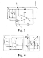
- Fig. 2 shows a further preferred embodiment of the oscillator circuit 1 according to the invention, in which the feedback resistor R 1 is omitted, but in the positive feedback branch, a current source I s , in particular a voltage-controlled current source I S , is used.
- a current source I s in particular a voltage-controlled current source I S .
- a "starting aid" which consists in that between the output 6 the operational amplifier 3 and the second terminal 5 of the resonant circuit 2, an ohmic voltage divider, consisting of the resistors R 2 and R 3 is provided, and the center tap 8 of the voltage divider R 2, R 3 is connected to the inverting input of the operational amplifier 3 and the branch of the voltage divider R 2, R 3 between the center tap 8 and the second terminal 5 of the resonant circuit 2 via a capacitor C 1 is short-circuited ac current.
- the circuit thus has only equal magnitudes, the voltage divider R 2 , R 3 is fully effective, with the result that the negative voltage at the output 6 of the operational amplifier, the potential at the inverting Input of the operational amplifier 3 pulls below the potential which may at worst lie against the non-inverting input of the operational amplifier 3, wherein the voltage applied there is determined by the voltage divider formed by the resistors R 1 and R 5 .
- the embodiment according to the invention according to FIG. 4 shows an application of the oscillator circuit 1 according to the invention, as is frequently found in contactless sensors.
- the oscillator circuit 1 is connected downstream of a demodulator circuit 9, the task of which is to recover from the amplitude-modulated oscillation of the resonant circuit 2 the envelope curve - that is to say the actual influencing information obtained by the resonant circuit.
- the demodulator circuit 9 provides an impedance converter 10, an electronic switch 11 and a low-pass filter 12 for this purpose.
- the input of the impedance converter 10 is connected to the analog output 7 of the oscillator circuit 1 is connected and the electronic switch 11 is actuated by the binary signal at the output 6 of the operational amplifier 3, so that in the closed state of the electronic switch 11, the output signal of the impedance converter 10 is fed to the input of the low-pass filter 12.
- the impedance converter 10 is realized by an emitter follower circuit T 1 , R 4 , the electronic switch 11 by a MOS field effect transistor T 2 and the low-pass filter 12 by an RC element R 5 , C 2 .
Landscapes
- Inductance-Capacitance Distribution Constants And Capacitance-Resistance Oscillators (AREA)
- Electronic Switches (AREA)
Applications Claiming Priority (1)
| Application Number | Priority Date | Filing Date | Title |
|---|---|---|---|
| DE102004034190A DE102004034190B4 (de) | 2004-07-14 | 2004-07-14 | Oszillatorschaltung für einen Sensor |
Publications (2)
| Publication Number | Publication Date |
|---|---|
| EP1617562A2 true EP1617562A2 (fr) | 2006-01-18 |
| EP1617562A3 EP1617562A3 (fr) | 2009-09-30 |
Family
ID=35240887
Family Applications (1)
| Application Number | Title | Priority Date | Filing Date |
|---|---|---|---|
| EP05011777A Withdrawn EP1617562A3 (fr) | 2004-07-14 | 2005-06-01 | Circuit d'oscillateur |
Country Status (3)
| Country | Link |
|---|---|
| US (1) | US7561000B2 (fr) |
| EP (1) | EP1617562A3 (fr) |
| DE (1) | DE102004034190B4 (fr) |
Cited By (1)
| Publication number | Priority date | Publication date | Assignee | Title |
|---|---|---|---|---|
| DE102020130518A1 (de) | 2020-11-18 | 2022-05-19 | Balluff Gmbh | Oszillatorschaltung |
Families Citing this family (13)
| Publication number | Priority date | Publication date | Assignee | Title |
|---|---|---|---|---|
| NL1033148C2 (nl) * | 2006-12-29 | 2008-07-01 | Univ Delft Tech | Elektrische meetinrichting, werkwijze en computer programma product. |
| DE102008062302B4 (de) | 2007-12-20 | 2015-01-22 | Robert Buck | Verfahren zur Bestimmung des Maßes der Änderung der Bedämpfung einer Last sowie Anordnung zur Durchführung eines derartigen Verfahrens |
| US8384378B2 (en) * | 2009-02-27 | 2013-02-26 | Kimberly-Clark Worldwide, Inc. | Conductivity sensor |
| US8452388B2 (en) * | 2009-02-27 | 2013-05-28 | Kimberly-Clark Worldwide, Inc. | Apparatus and method for assessing vascular health |
| US8258777B2 (en) * | 2009-09-04 | 2012-09-04 | Weihua Chen | Inductive proximity sensor |
| JP5083287B2 (ja) * | 2009-09-11 | 2012-11-28 | セイコーエプソン株式会社 | 検出装置、物理量測定装置及び電子機器 |
| WO2012095111A1 (fr) * | 2011-01-13 | 2012-07-19 | Vestas Wind Systems A/S | Essai d'un système de protection d'une turbine d'éolienne contre les survitesses |
| DE202011001009U1 (de) * | 2011-04-29 | 2012-07-31 | Mel Mikroelektronik Gmbh | Sensorsystem mit induktivem Näherungsschalter |
| DE102012208082B3 (de) * | 2012-05-15 | 2013-08-22 | Ifm Electronic Gmbh | Induktiver Näherungsschalter mit einem Komparator |
| EP2911299B1 (fr) | 2014-02-20 | 2020-08-26 | Pepperl + Fuchs GmbH | Procédé et circuit d'exploitation d'une grandeur de mesure physique enregistrée par un capteur |
| US20160268970A1 (en) * | 2015-03-10 | 2016-09-15 | Fred Mirow | Sensitivity variable loop gain oscillator sensor system |
| CN206533351U (zh) * | 2016-11-07 | 2017-09-29 | 欧姆龙株式会社 | 检测电路及开关结构 |
| JP6923849B2 (ja) * | 2018-01-29 | 2021-08-25 | オムロン株式会社 | 近接センサ及び検出距離の変更方法 |
Family Cites Families (7)
| Publication number | Priority date | Publication date | Assignee | Title |
|---|---|---|---|---|
| DE1956645B2 (de) * | 1969-11-11 | 1977-03-10 | Siemens AG, 1000 Berlin und 8000 München | Analogsignal-schalter unter verwendung eines feldeffekt-transistors |
| US4347740A (en) * | 1979-11-13 | 1982-09-07 | Magnetrol International, Incorporated | Capacitive level sensing device |
| DE3320509C2 (de) * | 1983-06-07 | 1994-02-17 | Merten Kg Pulsotronic | Elektronischer Näherungsschalter |
| US4617534A (en) * | 1984-03-23 | 1986-10-14 | U.S. Philips Corporation | High-speed switched oscillator |
| US5063359A (en) * | 1990-11-15 | 1991-11-05 | At&T Bell Laboratories | Low-jitter oscillator |
| US6215365B1 (en) * | 1999-06-04 | 2001-04-10 | Pepperl + Fuchs | Inductive proximity sensor oscillator |
| DE10137091A1 (de) * | 2001-07-30 | 2003-02-13 | Sick Ag | Induktiver Näherungssensor |
-
2004
- 2004-07-14 DE DE102004034190A patent/DE102004034190B4/de not_active Expired - Lifetime
-
2005
- 2005-06-01 EP EP05011777A patent/EP1617562A3/fr not_active Withdrawn
- 2005-07-14 US US11/180,904 patent/US7561000B2/en active Active
Non-Patent Citations (2)
| Title |
|---|
| SCHIFF, A.: "DIE BIBLIOTHEK DER TECHNIK", vol. 24, 1989, VERLAG MODERNE INDU- STRIE, article "Induktive und kapaziti- ve Sensoren" |
| TIETZE, U.; SCHENK CH.: "HALBLEITER-SCHALTUNGS-TECHNIK", vol. 12, 2002, SPRINGER VERLAG, pages: 874 |
Cited By (1)
| Publication number | Priority date | Publication date | Assignee | Title |
|---|---|---|---|---|
| DE102020130518A1 (de) | 2020-11-18 | 2022-05-19 | Balluff Gmbh | Oszillatorschaltung |
Also Published As
| Publication number | Publication date |
|---|---|
| US7561000B2 (en) | 2009-07-14 |
| EP1617562A3 (fr) | 2009-09-30 |
| DE102004034190A1 (de) | 2006-02-09 |
| DE102004034190B4 (de) | 2011-12-29 |
| US20060012443A1 (en) | 2006-01-19 |
Similar Documents
| Publication | Publication Date | Title |
|---|---|---|
| DE3129306C2 (de) | Mikrowellen-Oszillator mit Feldeffekt-Transistor | |
| DE102004034190B4 (de) | Oszillatorschaltung für einen Sensor | |
| DE2708021C3 (de) | Schaltungsanordnung in integrierter CMOS-Technik zur Regelung der Speisespannung für eine Last | |
| EP0320442B1 (fr) | Application d'un résonateur diélectrique d'hyperfréquence et circuit de détection | |
| DE102014220406A1 (de) | Treiberschaltung für eine Induktivität und aktive Sendeeinrichtung mit einer Treiberschaltung | |
| DE102011087116A1 (de) | Frequenzvervielfacher | |
| DE102004017497A1 (de) | Verstärkerschaltung | |
| DE2140056C3 (de) | Berührungslos steuerbarer Näherungsschalter | |
| EP2979311B1 (fr) | Agencement de circuit et procédé d'excitation d'un transformateur piézoélectrique | |
| WO2000067040A1 (fr) | Capteur de courant fonctionnant selon le principe de la compensation | |
| EP2599216B1 (fr) | Circuiterie dotée de capacités de compensation pour générer des oscillations hyperfréquence | |
| DE10345234B3 (de) | Oszillatoranordnung mit erhöhter EMI-Robustheit | |
| DE10310174A1 (de) | Schaltungsanordnung zur Gleichrichtung der Ausgangsspannung eines von einem Oszillator gespeisten Sensors | |
| EP2911299B1 (fr) | Procédé et circuit d'exploitation d'une grandeur de mesure physique enregistrée par un capteur | |
| DE1766295B2 (de) | Schaltbarer Oszillator mit wenigstens einem Transistor | |
| DE10328113B4 (de) | Vorrichtung zum Betreiben einer schwingfähigen Einheit eines Vibrationsresonators | |
| EP1282232A1 (fr) | Capteur de proximité inductif | |
| DE102009057107B4 (de) | Verfahren und Schaltungsanordnung zum Steuern von Schalttransistoren einer integrierten Schaltung | |
| DE69316986T2 (de) | Positionsensoren | |
| EP3641133B1 (fr) | Dispositif pilote | |
| DE69702267T2 (de) | Elektromagnetisches aufhängungsgerät und verfahren zu dessen steuerung | |
| DE10228694A1 (de) | Wien-Robinson-Oszillator | |
| DE102023107760A1 (de) | Induktiver Näherungsschalter und Verfahren zum Betreiben eines induktiven Näherungsschalters | |
| EP0774831A2 (fr) | Agencement de circuit pour générer une fréquence d'horloge pour un système de transmission de données | |
| DE1623109C3 (de) | Elektronischer Näherungsinitiator |
Legal Events
| Date | Code | Title | Description |
|---|---|---|---|
| PUAI | Public reference made under article 153(3) epc to a published international application that has entered the european phase |
Free format text: ORIGINAL CODE: 0009012 |
|
| AK | Designated contracting states |
Kind code of ref document: A2 Designated state(s): AT BE BG CH CY CZ DE DK EE ES FI FR GB GR HU IE IS IT LI LT LU MC NL PL PT RO SE SI SK TR |
|
| AX | Request for extension of the european patent |
Extension state: AL BA HR LV MK YU |
|
| PUAL | Search report despatched |
Free format text: ORIGINAL CODE: 0009013 |
|
| AK | Designated contracting states |
Kind code of ref document: A3 Designated state(s): AT BE BG CH CY CZ DE DK EE ES FI FR GB GR HU IE IS IT LI LT LU MC NL PL PT RO SE SI SK TR |
|
| AX | Request for extension of the european patent |
Extension state: AL BA HR LV MK YU |
|
| 17P | Request for examination filed |
Effective date: 20100317 |
|
| AKX | Designation fees paid |
Designated state(s): AT BE BG CH CY CZ DE DK EE ES FI FR GB GR HU IE IS IT LI LT LU MC NL PL PT RO SE SI SK TR |
|
| RAP1 | Party data changed (applicant data changed or rights of an application transferred) |
Owner name: IFM ELECTRONIC GMBH |
|
| 17Q | First examination report despatched |
Effective date: 20110822 |
|
| GRAP | Despatch of communication of intention to grant a patent |
Free format text: ORIGINAL CODE: EPIDOSNIGR1 |
|
| STAA | Information on the status of an ep patent application or granted ep patent |
Free format text: STATUS: THE APPLICATION IS DEEMED TO BE WITHDRAWN |
|
| 18D | Application deemed to be withdrawn |
Effective date: 20121120 |